EP0244848A1 - Procédé pour aplanir des couches minérales utilisées comme couches isolantes intermédiaires dans des interconnexions multi-couches - Google Patents
Procédé pour aplanir des couches minérales utilisées comme couches isolantes intermédiaires dans des interconnexions multi-couches Download PDFInfo
- Publication number
- EP0244848A1 EP0244848A1 EP87106561A EP87106561A EP0244848A1 EP 0244848 A1 EP0244848 A1 EP 0244848A1 EP 87106561 A EP87106561 A EP 87106561A EP 87106561 A EP87106561 A EP 87106561A EP 0244848 A1 EP0244848 A1 EP 0244848A1
- Authority
- EP
- European Patent Office
- Prior art keywords
- layer
- inorganic insulation
- insulation layer
- organic auxiliary
- auxiliary layer
- Prior art date
- Legal status (The legal status is an assumption and is not a legal conclusion. Google has not performed a legal analysis and makes no representation as to the accuracy of the status listed.)
- Withdrawn
Links
Images

Classifications
-
- H—ELECTRICITY
- H10—SEMICONDUCTOR DEVICES; ELECTRIC SOLID-STATE DEVICES NOT OTHERWISE PROVIDED FOR
- H10W—GENERIC PACKAGES, INTERCONNECTIONS, CONNECTORS OR OTHER CONSTRUCTIONAL DETAILS OF DEVICES COVERED BY CLASS H10
- H10W20/00—Interconnections in chips, wafers or substrates
- H10W20/01—Manufacture or treatment
- H10W20/071—Manufacture or treatment of dielectric parts thereof
- H10W20/092—Manufacture or treatment of dielectric parts thereof by smoothing the dielectric parts
-
- H—ELECTRICITY
- H10—SEMICONDUCTOR DEVICES; ELECTRIC SOLID-STATE DEVICES NOT OTHERWISE PROVIDED FOR
- H10P—GENERIC PROCESSES OR APPARATUS FOR THE MANUFACTURE OR TREATMENT OF DEVICES COVERED BY CLASS H10
- H10P50/00—Etching of wafers, substrates or parts of devices
- H10P50/20—Dry etching; Plasma etching; Reactive-ion etching
- H10P50/28—Dry etching; Plasma etching; Reactive-ion etching of insulating materials
- H10P50/282—Dry etching; Plasma etching; Reactive-ion etching of insulating materials of inorganic materials
- H10P50/283—Dry etching; Plasma etching; Reactive-ion etching of insulating materials of inorganic materials by chemical means
-
- H—ELECTRICITY
- H10—SEMICONDUCTOR DEVICES; ELECTRIC SOLID-STATE DEVICES NOT OTHERWISE PROVIDED FOR
- H10P—GENERIC PROCESSES OR APPARATUS FOR THE MANUFACTURE OR TREATMENT OF DEVICES COVERED BY CLASS H10
- H10P95/00—Generic processes or apparatus for manufacture or treatments not covered by the other groups of this subclass
- H10P95/06—Planarisation of inorganic insulating materials
- H10P95/062—Planarisation of inorganic insulating materials involving a dielectric removal step
- H10P95/064—Planarisation of inorganic insulating materials involving a dielectric removal step the removal being chemical etching
Definitions
- the invention relates to a method for planarizing the surface of an inorganic insulation layer, such as is used as an intermediate layer for multilayer metallizations of highly integrated semiconductor circuits, in which the planarization process is supported by the participation of an organic auxiliary layer and an etch-back process.
- the object of the invention is therefore to provide a method with which an almost flat surface is achieved after the production of the inorganic insulation layer.
- the method should be applicable for structure distances of less than 2 ⁇ m and structure heights of less than 1 ⁇ m.
- This process control solves the problem in a simple manner, that is, narrow gaps are also filled with the insulation material, since the process is repeated until all the gaps into which the above-mentioned layers can be deposited are filled.
- the use of the organic auxiliary layer and its complete removal by etching in the magnetron etching system ensures that the full gap width is retained and the inorganic insulation layer in the gap floor is not thinned.
- the method according to the teaching of the invention offers the possibility of producing highly integrated semiconductor circuits, in particular CMOS modules, with more than three wiring levels even on uneven substrates and with structure spacings of less than 2 ⁇ m. Electromigration effects and etching residues do not occur; the service life for current-loaded conductor tracks is tripled.
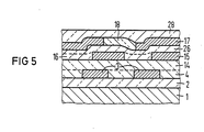
- the reference numeral 15 denotes the second metallization, 16 and 26 the second intermediate oxide layer, 17 the third metallization and 18 and 28 the third intermediate oxide layer or passivation layer.
- FIGS. 1 and 5 clearly shows the advantages of the method according to the invention.
Landscapes
- Internal Circuitry In Semiconductor Integrated Circuit Devices (AREA)
Applications Claiming Priority (2)
| Application Number | Priority Date | Filing Date | Title |
|---|---|---|---|
| DE3615451 | 1986-05-07 | ||
| DE3615451 | 1986-05-07 |
Publications (1)
| Publication Number | Publication Date |
|---|---|
| EP0244848A1 true EP0244848A1 (fr) | 1987-11-11 |
Family
ID=6300347
Family Applications (1)
| Application Number | Title | Priority Date | Filing Date |
|---|---|---|---|
| EP87106561A Withdrawn EP0244848A1 (fr) | 1986-05-07 | 1987-05-06 | Procédé pour aplanir des couches minérales utilisées comme couches isolantes intermédiaires dans des interconnexions multi-couches |
Country Status (1)
| Country | Link |
|---|---|
| EP (1) | EP0244848A1 (fr) |
Cited By (4)
| Publication number | Priority date | Publication date | Assignee | Title |
|---|---|---|---|---|
| WO1989006046A1 (fr) * | 1987-12-19 | 1989-06-29 | Plessey Overseas Limited | Dispositifs semiconducteurs fabriques sur des tranches soi (silicium sur isolateur) |
| EP0411795A1 (fr) * | 1989-07-31 | 1991-02-06 | AT&T Corp. | Depôt anisotrope de dioxyde de silicium |
| EP0482247A1 (fr) * | 1990-10-26 | 1992-04-29 | International Business Machines Corporation | Procédé de fabrication d'une structure de circuit intégrée à une configuration dense de métallisation multicouche |
| GB2265254A (en) * | 1992-03-17 | 1993-09-22 | Mitsubishi Electric Corp | A semiconductor device with planarized insulating layers |
Citations (4)
| Publication number | Priority date | Publication date | Assignee | Title |
|---|---|---|---|---|
| EP0023146A2 (fr) * | 1979-07-23 | 1981-01-28 | Fujitsu Limited | Procédé pour la fabrication d'un dispositif semiconducteur, dans lequel sont formées des premières et secondes couches |
| WO1984004996A1 (fr) * | 1983-06-13 | 1984-12-20 | Ncr Co | Procede de fabrication de structures semi-conductrices |
| WO1985004623A1 (fr) * | 1984-04-04 | 1985-10-24 | Advanced Micro Devices, Inc. | Procede en deux etapes permettant de rendre planes des structures de circuits integres en vue de leur metallisation multicouche |
| EP0216425A2 (fr) * | 1985-09-20 | 1987-04-01 | Philips Composants | Procédé pour aplanir la surface d'un dispositif semiconducteur utilisant du nitrure de silicium comme materiau isolant |
-
1987
- 1987-05-06 EP EP87106561A patent/EP0244848A1/fr not_active Withdrawn
Patent Citations (4)
| Publication number | Priority date | Publication date | Assignee | Title |
|---|---|---|---|---|
| EP0023146A2 (fr) * | 1979-07-23 | 1981-01-28 | Fujitsu Limited | Procédé pour la fabrication d'un dispositif semiconducteur, dans lequel sont formées des premières et secondes couches |
| WO1984004996A1 (fr) * | 1983-06-13 | 1984-12-20 | Ncr Co | Procede de fabrication de structures semi-conductrices |
| WO1985004623A1 (fr) * | 1984-04-04 | 1985-10-24 | Advanced Micro Devices, Inc. | Procede en deux etapes permettant de rendre planes des structures de circuits integres en vue de leur metallisation multicouche |
| EP0216425A2 (fr) * | 1985-09-20 | 1987-04-01 | Philips Composants | Procédé pour aplanir la surface d'un dispositif semiconducteur utilisant du nitrure de silicium comme materiau isolant |
Non-Patent Citations (1)
| Title |
|---|
| EXTENDED ABSTRACTS, Band 83, Nr. 2, 9.-14. Oktober 1983, Seite 327, Princeton, US; K.H. OH et al.: "Bird's head smoothing by two-step plasma etch" * |
Cited By (7)
| Publication number | Priority date | Publication date | Assignee | Title |
|---|---|---|---|---|
| WO1989006046A1 (fr) * | 1987-12-19 | 1989-06-29 | Plessey Overseas Limited | Dispositifs semiconducteurs fabriques sur des tranches soi (silicium sur isolateur) |
| EP0411795A1 (fr) * | 1989-07-31 | 1991-02-06 | AT&T Corp. | Depôt anisotrope de dioxyde de silicium |
| EP0482247A1 (fr) * | 1990-10-26 | 1992-04-29 | International Business Machines Corporation | Procédé de fabrication d'une structure de circuit intégrée à une configuration dense de métallisation multicouche |
| GB2265254A (en) * | 1992-03-17 | 1993-09-22 | Mitsubishi Electric Corp | A semiconductor device with planarized insulating layers |
| US5479054A (en) * | 1992-03-17 | 1995-12-26 | Mitsubishi Denki Kabushiki Kaisha | Semiconductor device with improved planarization properties |
| GB2265254B (en) * | 1992-03-17 | 1996-03-13 | Mitsubishi Electric Corp | A semiconductor chip and a method of manufacture thereof |
| US5930674A (en) * | 1992-03-17 | 1999-07-27 | Mitsubishi Denki Kabushiki Kaisha | Semiconductor device with improved planarization properties |
Similar Documents
| Publication | Publication Date | Title |
|---|---|---|
| DE10230088B4 (de) | Verfahren zum Herstellen einer Halbleitervorrichtung | |
| DE69425636T2 (de) | Planarisierungstechnik für eine integrierte Schaltung | |
| DE69222586T2 (de) | Mehrlagige Verbindungsstruktur für eine Halbleiter- vorrichtung und Verfahren zu ihrer Herstellung | |
| EP0842532B1 (fr) | Procede de production d'une couche d'espacement dans une structure | |
| DE68923305T2 (de) | Elektrische Leitungen für elektronische Bauelemente. | |
| DE2430692C2 (de) | Verfahren zum Herstellen von Verbindungslöchern in Isolierschichten | |
| DE69025801T2 (de) | Verfahren zum Formen von elektrischen Kontakten zwischen Verbindungsleiterschichten auf verschiedenen Ebenen | |
| DE2832740C2 (de) | Verfahren zum Herstellen einer Halbleiteranordnung mit einer Mehrebenenverdrahtung | |
| DE3241895A1 (de) | Verfahren zur passivierung der oberflaeche eines halbleiterbauteils | |
| WO2010006916A1 (fr) | Procédé de fabrication d’un composant semi-conducteur et composant semi-conducteur | |
| DE2636971C2 (de) | Verfahren zum Herstellen einer isolierenden Schicht mit ebener Oberfläche auf einer unebenen Oberfläche eines Substrats | |
| DE69627233T2 (de) | Verfahren zum Herstellen einer Halbleiteranordnung mit einer Mehrschichtverbindungsstruktur, mit einem verbesserten Schritt zum Herstellen einer dielektrischen Zwischenschicht | |
| DE69212853T2 (de) | Verfahren zur Planarizierung einer Oberfläche von Bauelementen mit integrierter Schaltung | |
| DE2432719A1 (de) | Verfahren zum erzeugen von feinen strukturen aus aufdampfbaren materialien auf einer unterlage | |
| DE69724965T2 (de) | Verfahren zur vereinfachung der herstellung eines dielektrischen zwischenschicht-stapels | |
| EP0211318B1 (fr) | Procédé de remplissage sélectif de trous de contact formés par attaque dans des couches d'isolation avec des matériaux électriquement conducteurs pour la fabrication de circuits semi-conducteurs à haute densité d'intégration et appareil utilisé pour ce procédé | |
| DE3234907A1 (de) | Verfahren zum herstellen einer monolithisch integrierten schaltung | |
| EP0244848A1 (fr) | Procédé pour aplanir des couches minérales utilisées comme couches isolantes intermédiaires dans des interconnexions multi-couches | |
| EP0177845A1 (fr) | Circuit intégré à métallisation multicouche et procédé pour sa fabrication | |
| EP1198828A1 (fr) | Procede de production d'un composant de stockage a semi-conducteur | |
| EP0103690B1 (fr) | Procédé de fabrication d'une couche isolante entre des couches de métallisation de circuits semi-conducteurs intégrés | |
| DE19723708A1 (de) | Verfahren zur Herstellung einer mehrschichtigen Verdrahtung in einem Halbleiterbauelement | |
| DE2753489A1 (de) | Monolithisch integrierte halbleiterschaltung | |
| DE3345040A1 (de) | Verfahren zur herstellung einer eingeebneten, die zwei metallisierungen trennenden anorganischen isolationsschicht unter verwendung von polyimid | |
| DE3784902T2 (de) | Verfahren zur herstellung von verbindungslinien und von kreuzungspunkten verschiedener metallisierungsebenen auf einer integrierten schaltung. |
Legal Events
| Date | Code | Title | Description |
|---|---|---|---|
| PUAI | Public reference made under article 153(3) epc to a published international application that has entered the european phase |
Free format text: ORIGINAL CODE: 0009012 |
|
| AK | Designated contracting states |
Kind code of ref document: A1 Designated state(s): BE DE FR GB NL |
|
| STAA | Information on the status of an ep patent application or granted ep patent |
Free format text: STATUS: THE APPLICATION IS DEEMED TO BE WITHDRAWN |
|
| 18D | Application deemed to be withdrawn |
Effective date: 19880512 |
|
| RIN1 | Information on inventor provided before grant (corrected) |
Inventor name: GREWAL, VIRINDER, DR. Inventor name: FRITZSCHE, HANSJOERG, DR. |