EP0245747A2 - Dispositif pour diriger une pluralité de transistors de puissance à effet de champ reliés en parallèle - Google Patents
Dispositif pour diriger une pluralité de transistors de puissance à effet de champ reliés en parallèle Download PDFInfo
- Publication number
- EP0245747A2 EP0245747A2 EP87106450A EP87106450A EP0245747A2 EP 0245747 A2 EP0245747 A2 EP 0245747A2 EP 87106450 A EP87106450 A EP 87106450A EP 87106450 A EP87106450 A EP 87106450A EP 0245747 A2 EP0245747 A2 EP 0245747A2
- Authority
- EP
- European Patent Office
- Prior art keywords
- transistors
- group
- mounting board
- control
- busbar
- Prior art date
- Legal status (The legal status is an assumption and is not a legal conclusion. Google has not performed a legal analysis and makes no representation as to the accuracy of the status listed.)
- Withdrawn
Links
Images
Classifications
-
- H—ELECTRICITY
- H10—SEMICONDUCTOR DEVICES; ELECTRIC SOLID-STATE DEVICES NOT OTHERWISE PROVIDED FOR
- H10W—GENERIC PACKAGES, INTERCONNECTIONS, CONNECTORS OR OTHER CONSTRUCTIONAL DETAILS OF DEVICES COVERED BY CLASS H10
- H10W90/00—Package configurations
-
- H—ELECTRICITY
- H05—ELECTRIC TECHNIQUES NOT OTHERWISE PROVIDED FOR
- H05K—PRINTED CIRCUITS; CASINGS OR CONSTRUCTIONAL DETAILS OF ELECTRIC APPARATUS; MANUFACTURE OF ASSEMBLAGES OF ELECTRICAL COMPONENTS
- H05K1/00—Printed circuits
- H05K1/02—Details
- H05K1/0213—Electrical arrangements not otherwise provided for
- H05K1/0263—High current adaptations, e.g. printed high current conductors or using auxiliary non-printed means; Fine and coarse circuit patterns on one circuit board
-
- H—ELECTRICITY
- H05—ELECTRIC TECHNIQUES NOT OTHERWISE PROVIDED FOR
- H05K—PRINTED CIRCUITS; CASINGS OR CONSTRUCTIONAL DETAILS OF ELECTRIC APPARATUS; MANUFACTURE OF ASSEMBLAGES OF ELECTRICAL COMPONENTS
- H05K1/00—Printed circuits
- H05K1/18—Printed circuits structurally associated with non-printed electric components
Definitions
- the invention relates to an arrangement for driving a plurality of power field effect transistors connected in parallel according to the preamble of claim 1.
- Power electronics often use MOS-FET power transistors for the regulated current and voltage supply of motors.
- a DC motor can be operated, for example, via a four-quadrant actuator equipped with MOS-FET in both directions of rotation at different speeds from a DC voltage source.
- Field effect transistors particularly in the partial load range, behave more favorably in terms of power loss and required drive power than bipolar transistors. Difficulties arise, however, when relatively high currents are to be switched, since the available power MOSFETs are only suitable for relatively low currents.
- Common and simultaneous control can be remedied. It should be noted, however, that all parallel field effect transistors must be controlled exactly symmetrically in order to avoid thermal overloading of individual transistors with subsequent destruction.
- the invention has for its object to provide an arrangement for controlling a plurality of power field effect transistors connected in parallel of the type mentioned, which ensures an exactly symmetrical control of all parallel transistors.
- the advantages that can be achieved with the invention are, in particular, that the specified arrangement enables a very precise, simultaneous control of all field-effect transistors connected in parallel. Due to the subdivision of the transistors into individual groups, a "star-shaped" control of the individual transistors of each group is guaranteed, i.e. control with control paths of the same length. The individual groups are in turn controlled in a "star shape" via bus lines of equal length, so that an exactly symmetrical control of all parallel transistors is achieved.
- the arrangement is advantageously compact and has short lines both in the control part and in the load part. Further advantages are evident from the description below.
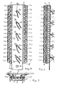
- FIG. 1 shows a top view of a bridge branch of a four-quadrant actuator.
- the bridge branch has, for example, 30 MOS-FET power transistors T1, T2 ... T30 connected in parallel, which are to be driven jointly and simultaneously between gate G and source S.
- the transistors are divided into two opposite rows of 15 each.
- An elongated, U-shaped copper busbar 1 is provided for the common power connection of all source connections S of the power transistors T1 ... T30.
- the two bent side parts of the busbar 1 are punched out in a triangular shape, so that there are at least 15 triangular fastening corners 2 on each side for the source load connections of the 30 power transistors T1 ... T30.
- the 30 MOS-FET power transistors T1 ... T30 are combined in 5 groups of 6 transistors each.
- the transistors T1 ... T6, T7 ... T12, T13 ... T18, T19 ... T24 and T25 ... T30 each form a group.
- Each group has two opposite rows of 3 transistors each.
- the central part of the busbar 1 is provided with central bores 3a, b, c, d, e, the central bore 3a belonging to group T1 ... T6, the central bore 3b belonging to group T7 ... T12 etc. is.
- Another hole 3f in the extended end part of the busbar 1 serves to form a common source-load connection.
- Two drive lines are led through each center hole 3a-e, specifically a common gate connecting line 4a-e and a common source-connecting line 5a-e. The further interconnection of these control lines is described in FIG. 6.
- a circuit board 6 is provided to connect the transistor connections and to set up the individual circuitry for the transistors.
- the mounting board 6 partially covered by the busbar 1 in FIG. 1 is coated on both sides with conductor tracks and has components 7 of the individual circuitry on its upper side, in particular resistors and capacitors for du / dt limitation and gate resistors for suppressing vibrations between the gate Connections of the transistors connected in parallel.
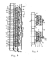
- FIG. 2 shows a side view of the long side of a bridge branch.
- the busbar 1 with the triangular fastening corners 2 can be seen in the bent side part.
- the connecting wires 8 of the power transistors (they are the transistors T2, T4, T6 ... T30)) are soldered onto the mounting board 6. Individual components 7 of the assembly board 6 are shown. Furthermore, the assignment of one common gate connection line 4a-e and one common source-source connection line 5a-e can be seen in each case one of the 5 transistor groups.
- FIG. 4 shows a side view of the long side of a half bridge consisting of two bridge branches.
- the copper busbar 1 with the mounting corners 2, the common gate connection lines 4a-e, the common source connection lines 5a-e, the circuit board 6 for the transistors and the individual circuitry, the components 7 of the circuit board 6, the transistors recognizable with their connecting wires 8 and the heat sink 9 for a bridge branch.
- the busbar 1 there is a mounting board 11 for the group connection of the transistors (the transistors T2, T4 ... T30 are shown).
- the components 12 (resistors, capacitors, diodes) of the group scarf each serve to connect a group consisting of 6 transistors (transistor groups T1 ... T6, T7 ... T12 etc.).
- the circuit serves to limit the switch-off voltage peaks.
- the circuit board 11 for the group connection there is a circuit board 13 for the modulation with components 14 for implementing control and regulating devices for the transistors of the four-quadrant actuator.
- the heat sink 9 can be fastened to a further, superordinate and ribbed heat sink with the aid of mounting screws, a plastic film 16 being located between the heat sink 9 and the higher-level heat sink for insulation against the drain potential of the heat sink 9.
- the heat sink 9 is provided with a drain load connection 17 and the busbar 1 with a source load connection 18 (see also hole 3f in FIG. 1).
- FIG. 5 shows a side view of the narrow side of a half-bridge, the two bridge branches being recognizable.
- the busbars 1 with the mounting corners 2 soldered to the printed circuit boards 6, the common gate connecting lines 4a, the common source connecting lines 5a, the components 7 of the boards 6, the boards 11 for group connection with components 12, the two bridge branches common circuit board 13 for the control, the two separate heat sinks 9 and the transistors mounted thereon.
- Bolts 19 are provided for the mechanical connection between busbar 1, mounting board 11 for group wiring and mounting board 13 for control.
- the common gate connection lines 4a-e and the common source connection lines 5a-e are each for reasons of the exact symmetrical control of all transistors connected in parallel and twisted together.
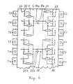
- FIG. 6 shows a top view of a printed circuit board 6 for transistors and individual wiring.
- the connecting wires 8 of the transistors are inserted and soldered through connection bores 20 arranged in the lateral area of the mounting board 6.
- the source connections S of the transistors are each connected to further connection bores 21 for the fastening corners 2 of the busbar 1 via short conductor tracks.
- the mounting corners 2 are plugged onto these connection bores 21 and soldered.
- the gate connections G of all transistors in a group are led via conductor tracks 24 to a common collective gate connection 22a-e, each connection 22a-e being soldered to a connecting line 4a-e.
- a resistor (belonging to the components 7) is provided on the printed circuit board 6.
- the source connections S of all transistors in a group are led to a common common source connection 23a-e via conductor tracks 25 located partially on the rear side of the printed circuit board 2 coated on both sides, each connection 23a-e being soldered to a connection line 5a-e is.
- the conductor tracks 25 can in part also be carried out under the resistors.
- the drain connections D of the transistors are connected to individual wiring components via their own conductor tracks (not shown in FIG. 6 for reasons of clarity).
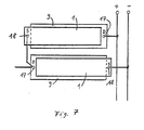
- FIG. 7 shows the arrangement of the two bridge branches of a half bridge.
- the bridge branches with busbars 1 and heat sink 3 are arranged one below the other rotated by 180 °.
- the drain-load connection 17 (on the heat sink) of the 1st bridge branch is connected to the positive voltage supply busbar.
- the source load connection 18 (on the busbar) of the 1st bridge branch is connected to the drain load connection 17 of the 2nd bridge branch.
- the source load connection 18 of the second bridge branch lies on the negative voltage supply busbar.
- the load is connected to the drain load connection 18 of the second bridge branch.
Landscapes
- Structures For Mounting Electric Components On Printed Circuit Boards (AREA)
- Inverter Devices (AREA)
- Rectifiers (AREA)
- Power Conversion In General (AREA)
Applications Claiming Priority (2)
| Application Number | Priority Date | Filing Date | Title |
|---|---|---|---|
| DE3615782 | 1986-05-10 | ||
| DE19863615782 DE3615782A1 (de) | 1986-05-10 | 1986-05-10 | Anordnung zur ansteuerung einer vielzahl parallelgeschalteter leistungs-feldeffekttransistoren |
Publications (2)
| Publication Number | Publication Date |
|---|---|
| EP0245747A2 true EP0245747A2 (fr) | 1987-11-19 |
| EP0245747A3 EP0245747A3 (fr) | 1989-04-26 |
Family
ID=6300558
Family Applications (1)
| Application Number | Title | Priority Date | Filing Date |
|---|---|---|---|
| EP87106450A Withdrawn EP0245747A3 (fr) | 1986-05-10 | 1987-05-05 | Dispositif pour diriger une pluralité de transistors de puissance à effet de champ reliés en parallèle |
Country Status (2)
| Country | Link |
|---|---|
| EP (1) | EP0245747A3 (fr) |
| DE (1) | DE3615782A1 (fr) |
Families Citing this family (2)
| Publication number | Priority date | Publication date | Assignee | Title |
|---|---|---|---|---|
| DE4007566C2 (de) * | 1990-03-09 | 1998-07-16 | Siemens Ag | Leistungsverstärker für die Speisung einer Induktivität mit geschalteten Transistoren |
| DE4401607C2 (de) * | 1994-01-20 | 1997-04-10 | Siemens Ag | Kühleinheit für Leistungshalbleiter |
Family Cites Families (4)
| Publication number | Priority date | Publication date | Assignee | Title |
|---|---|---|---|---|
| DE2739242C2 (de) * | 1977-08-31 | 1979-10-04 | Siemens Ag, 1000 Berlin Und 8000 Muenchen | Hochleistungsstromrichter |
| US4243894A (en) * | 1978-10-02 | 1981-01-06 | Eaton Corporation | Solid state motor control universal assembly means and method |
| US4454454A (en) * | 1983-05-13 | 1984-06-12 | Motorola, Inc. | MOSFET "H" Switch circuit for a DC motor |
| US4626750A (en) * | 1985-09-10 | 1986-12-02 | Curtis Instruments, Inc. | Solid state d.c. motor control |
-
1986
- 1986-05-10 DE DE19863615782 patent/DE3615782A1/de not_active Withdrawn
-
1987
- 1987-05-05 EP EP87106450A patent/EP0245747A3/fr not_active Withdrawn
Also Published As
| Publication number | Publication date |
|---|---|
| EP0245747A3 (fr) | 1989-04-26 |
| DE3615782A1 (de) | 1987-11-12 |
Similar Documents
| Publication | Publication Date | Title |
|---|---|---|
| DE102007013186B4 (de) | Halbleitermodul mit Halbleiterchips und Verfahren zur Herstellung desselben | |
| DE69532700T2 (de) | Steuerschaltungsmodul | |
| DE102015101086B4 (de) | Leistungshalbleitermodulanordnung | |
| DE102013104742B4 (de) | Verdrahtungselement und Halbleitermodul mit demselben | |
| EP1083599B1 (fr) | Dispositif semiconducteur de puissance | |
| DE102018132663B4 (de) | Schaltnetzteil | |
| DE102019114040A1 (de) | Dreistufiges Leistungsmodul | |
| DE102020007610A1 (de) | Motorantriebsvorrichtung mit Stromschiene | |
| DE3734067A1 (de) | Halbleitervorrichtung | |
| DE19838160A1 (de) | Umschaltanordnung | |
| EP0738008B1 (fr) | Module à semi-conducteur de puissance | |
| DE102021202174A1 (de) | Leistungsmodul, insbesondere für einen Wechselrichter für Elektromaschinen | |
| EP3557614A1 (fr) | Module de puissance pourvu d'un composant électronique de puissance sur une plaque de substrat et circuit électronique de puissance pourvu d'un tel module de puissance | |
| EP3719975A1 (fr) | Machine électrique | |
| EP1433204B1 (fr) | Dispositif a composants a semi-conducteur de puissance utilise pour la regulation de puissance de courants eleves, et utilisation dudit dispositif | |
| DE19706798B4 (de) | Halbleiter-Leistungsmodul | |
| EP3874917B1 (fr) | Circuit haute intensité | |
| EP1632117B1 (fr) | Composant electronique pour la commutation d'une alimentation electrique | |
| EP2091081B1 (fr) | Agencement de commutation doté d'une liaison par soudage | |
| EP0245747A2 (fr) | Dispositif pour diriger une pluralité de transistors de puissance à effet de champ reliés en parallèle | |
| DE10054489A1 (de) | Leistungs-Umrichtermodul | |
| DE19646396C2 (de) | Leistungshalbleitermodul für verschiedene Schaltungsvarianten | |
| DE102021213427B3 (de) | Kompaktes leistungswechselrichtermodul | |
| EP1764832A1 (fr) | Connexion de fixation pour des composants semiconducteurs de puissance | |
| DE102022207268A1 (de) | Inverteranordnung |
Legal Events
| Date | Code | Title | Description |
|---|---|---|---|
| PUAI | Public reference made under article 153(3) epc to a published international application that has entered the european phase |
Free format text: ORIGINAL CODE: 0009012 |
|
| AK | Designated contracting states |
Kind code of ref document: A2 Designated state(s): DE FR GB |
|
| RAP1 | Party data changed (applicant data changed or rights of an application transferred) |
Owner name: ASEA BROWN BOVERI AKTIENGESELLSCHAFT |
|
| PUAL | Search report despatched |
Free format text: ORIGINAL CODE: 0009013 |
|
| AK | Designated contracting states |
Kind code of ref document: A3 Designated state(s): DE FR GB |
|
| STAA | Information on the status of an ep patent application or granted ep patent |
Free format text: STATUS: THE APPLICATION IS DEEMED TO BE WITHDRAWN |
|
| 18D | Application deemed to be withdrawn |
Effective date: 19890601 |
|
| RIN1 | Information on inventor provided before grant (corrected) |
Inventor name: EBERT, REINHOLD, DIPL,-ING. Inventor name: BERTSCH, BRUNO, DIPL.-ING. |