EP0246689A2 - Circuit pour convertir des signaux à trois états en signaux binaires - Google Patents
Circuit pour convertir des signaux à trois états en signaux binaires Download PDFInfo
- Publication number
- EP0246689A2 EP0246689A2 EP87200843A EP87200843A EP0246689A2 EP 0246689 A2 EP0246689 A2 EP 0246689A2 EP 87200843 A EP87200843 A EP 87200843A EP 87200843 A EP87200843 A EP 87200843A EP 0246689 A2 EP0246689 A2 EP 0246689A2
- Authority
- EP
- European Patent Office
- Prior art keywords
- current
- output
- transistor
- input
- diode path
- Prior art date
- Legal status (The legal status is an assumption and is not a legal conclusion. Google has not performed a legal analysis and makes no representation as to the accuracy of the status listed.)
- Granted
Links
Images

Classifications
-
- H—ELECTRICITY
- H03—ELECTRONIC CIRCUITRY
- H03M—CODING; DECODING; CODE CONVERSION IN GENERAL
- H03M5/00—Conversion of the form of the representation of individual digits
- H03M5/02—Conversion to or from representation by pulses
- H03M5/16—Conversion to or from representation by pulses the pulses having three levels
Definitions
- the invention relates to a circuit arrangement for converting three-state signals into binary signals.
- a reference voltage range is defined by means of one or more ohmic voltage dividers, which lies between the potential of the positive and the negative supply voltage source.
- the object of the present invention is to create a circuit arrangement of the type mentioned at the outset without an ohmic voltage divider.
- a first direct current source connected on one side to the negative supply voltage connection and a second direct current source connected on one side to the positive supply voltage connection of a supply voltage source is provided and that the direct current sources with their free connection via a first or a second diode path with a common input and Via a third or fourth diode path, which are identical to the first or second diode path, are connected to a first or a second output transistor providing an output signal.
- the diode paths can consist of one or more diode elements connected in series and in the forward direction. If the potential at the common input is positive, the current of the first current source flows via the first diode path to the common input and no current is supplied to the output transistor coupled to the third diode path. In contrast, the current of the second current source in this case flows via the fourth diode path to the output transistor coupled to it.
- the current from the second current source flows via the second diode path to the common input.
- the fourth diode path remains currentless and no current is supplied to the output transistor coupled to it.
- the current supplied by the first current source flows via the third diode path to the output transistor coupled to it.
- the current of the two current sources only flows via the third and fourth diode paths to the two output transistors.
- the third or fourth diode path were connected directly to the input, for example the base of the associated output transistor, these transistors must have the opposite conductivity type and be connected to opposite supply voltage terminals.
- the potentials occurring at their outputs, in particular their collectors, which represent the binary output signals, would then depend on the level of the supply voltage. According to a further development of the invention, this can be avoided in that one of the third and fourth diode sections is direct and the other another is connected via a current mirror to the first or second output transistor and that the two output transistors are connected in the same way.
- the output transistors can then be connected to the same conductivity type and to the same supply voltage terminal.
- the further development of the invention provides that a switching transistor is connected in parallel to the input of at least one of the output transistors, which switching transistor can be controlled by the output current of a current mirror, the input current of which is via the first or the second diode path is flowing current.
- the input of an output transistor is short-circuited by the switching transistor connected in parallel, so that any residual currents are kept away from the output transistor.
- a preferred development of the invention provides that the transistors contained in the circuit, the emitters of which are connected to the negative supply voltage connection, are designed in I 2 L circuit technology and that the base current of these transistors is supplied by a common injector. With this configuration, crystal area can be saved when manufacturing the circuit using integrated circuit technology, and the currents of the current sources which are supplied by the injector can be relatively small.
- first direct current source S1 which has one connection to the negative supply voltage terminal, which is connected to ground
- second direct current source S2 which has one connection to the positive supply voltage terminal of a supply voltage source U.
- the respective other connection of the first and the second direct current source which supply a direct current of, for example, 1 pA, is connected via a first or a second diode path D1 or D2 to a common input, to which the three-state signal to be implemented is present .
- the free connection of the current sources S1 and S2 is also via a third diode path D3, which is identical to the first diode path Dl, or via a fourth diode path, which is identical to the second diode path, to the base terminal of a pnp output transistor Tp or an npn output transistor Tn, whose emitter is connected to the positive or negative supply voltage terminal and whose collector forms the output P or N of the circuit.
- An evaluation circuit is preferably connected to the outputs P and N, preferably using I 2 L circuit technology, which processes the binary output signals occurring on these signals.
- the common input I is connected to a switch Sw with three switch contacts, so that, depending on the position of the switch, the common input is either not connected or is connected to ground or the positive supply voltage.
- the bias voltage of the diode path D4 in the forward direction becomes greater than the corresponding voltage at the diode path D2.
- the current of the current source S2 then flows into the base of the transistor Tn and as a result appears at the output N.
- the output transistor Tp remains conductive as long as only the potential at the input I remains more negative than the base potential of the output transistor Tp.
- both output transistors carry an output current.
- input I remains unconnected, because then no current can flow through input I.
- a current flow from the current source S2 via the diode paths D2 and Dl to the current source S1 is excluded if the supply voltage U is greater than the sum of the base-emitter voltage of an output transistor, the forward voltage of one of the diode paths D3 or D4 and the Operating voltage of the current source S1 or S2.
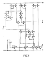
- the first current source S1 is formed by the collector-emitter path of an npn transistor T21, the emitter of which is connected to the negative supply voltage terminal and the collector of which is connected to the first and the third diode path.
- the first diode path is formed by the series connection of an npn transistor T17 which acts as a diode by connecting its collector to its base and a pnp transistor T15 which is likewise connected as a diode.
- the third diode path is constructed in the same way and consists of the series connection of the npn or pnp transistors Tl8 and T16 connected as diodes.
- the current source S2 is formed by the collector-emitter path of a transistor T3, the emitter of which is connected to the positive supply voltage terminal and the collector of which is connected to the second or fourth diode path.
- the second diode path is formed by the npn transistors T7 and T9 connected as a diode and the fourth diode path by the transistors T8 and Tll connected as a diode.
- a transistor T13 the base of which is connected to the second current source T3 via the fourth diode path T8, Tll and whose emitter is connected to ground, corresponds in function to the output transistor Tn.
- the third diode path is not connected directly to the base of the npn output transistor T23, whose emitter is connected to the negative supply voltage terminal, but to the input of one through the Transistors T5 and T6 formed current mirror, the output of which is connected to the base of transistor T23. Switching on the current mirror T5, T6 has the advantage that transistors of the same conductivity type can be used as output transistors.
- the first current source T21 is formed by an output of a current mirror, the input of which is an npn transistor T19 connected as a diode and the other output of which is a transistor T20, the base-emitter path of which is connected in parallel to the base-emitter path of the transistor T21.
- the collector of transistor T20 is connected to a pnp transistor T4 connected as a diode, the emitter of which is connected to the positive supply voltage terminal and which, together with transistor T3, forms a current mirror. Therefore, the current of the current source T3 is the same as the current of the current source T21.
- the input current of the current mirror T19, T20, T21 is supplied by a current source Q and has a size of e.g. 1 uA.
- the collector-emitter path of a transistor T12 or T22 is connected in parallel to the base-emitter paths of these transistors.
- the transistor T12 is fed by the output of a current mirror Tl, T2, the input of which is connected to the output of a further current mirror, the one transistor T10 and the transistor T9 connected as a diode which is connected to the heard second diode path includes.
- the transistor T22 is controlled by the collector current of a transistor T14 which, together with the transistor T15 of the first diode path connected as a diode, forms a current mirror.
- the output of the associated current mirror supplies a current which makes the transistor T22 or T12 conductive and short-circuits the input of the output transistor T13 or T23.
- the npn transistors T12, T13 and T19 ... T23, whose emitters are connected to the negative supply voltage terminal or ground, are advantageously implemented using I 2 L circuit technology.
- the current source Q can then be formed by a so-called injector transistor, which is suitable for generating small enough currents with a small crystal area, in particular if it is still used to supply 2L gates, which is part of a further circuit which is connected to the in Fig. 3 circuit shown is mounted on the same semiconductor substrate.
- the supply voltage of the circuit shown in FIG. 3 need only be three times the base-emitter voltage of one of the transistors plus the collector-emitter saturation voltage; if the transistors T7, T8 and T17, T18 connected as diodes are omitted, the supply voltage can be even lower by a base-emitter voltage and the switching can be even simpler with otherwise unchanged properties.
- the circuit can process not only stationary signals as provided by the circuit Sw in Fig. 1, but also AC signals.
Landscapes
- Engineering & Computer Science (AREA)
- Theoretical Computer Science (AREA)
- Logic Circuits (AREA)
- Amplifiers (AREA)
- Electronic Switches (AREA)
Applications Claiming Priority (2)
| Application Number | Priority Date | Filing Date | Title |
|---|---|---|---|
| DE19863616818 DE3616818A1 (de) | 1986-05-17 | 1986-05-17 | Schaltung zum umsetzen von drei-zustands-signalen in binaere signale |
| DE3616818 | 1986-05-17 |
Publications (3)
| Publication Number | Publication Date |
|---|---|
| EP0246689A2 true EP0246689A2 (fr) | 1987-11-25 |
| EP0246689A3 EP0246689A3 (en) | 1989-07-26 |
| EP0246689B1 EP0246689B1 (fr) | 1992-08-05 |
Family
ID=6301148
Family Applications (1)
| Application Number | Title | Priority Date | Filing Date |
|---|---|---|---|
| EP87200843A Expired - Lifetime EP0246689B1 (fr) | 1986-05-17 | 1987-05-11 | Circuit pour convertir des signaux à trois états en signaux binaires |
Country Status (4)
| Country | Link |
|---|---|
| US (1) | US4797581A (fr) |
| EP (1) | EP0246689B1 (fr) |
| JP (1) | JPH0793561B2 (fr) |
| DE (2) | DE3616818A1 (fr) |
Cited By (2)
| Publication number | Priority date | Publication date | Assignee | Title |
|---|---|---|---|---|
| GB2238695A (en) * | 1989-12-01 | 1991-06-05 | Philips Electronic Associated | Circuit arrangement for producing a binary signal |
| WO1998011669A1 (fr) * | 1996-09-13 | 1998-03-19 | Ut Automotive Dearborne, Inc. | Detection par commutateur trois etats au moyen d'un capteur de courant |
Families Citing this family (1)
| Publication number | Priority date | Publication date | Assignee | Title |
|---|---|---|---|---|
| JP2698225B2 (ja) * | 1991-04-15 | 1998-01-19 | シャープ株式会社 | サンプルホールド回路 |
Family Cites Families (4)
| Publication number | Priority date | Publication date | Assignee | Title |
|---|---|---|---|---|
| GB875381A (en) * | 1958-11-27 | 1961-08-16 | Ass Elect Ind | Improvements relating to electronic switching circuits |
| FR2102970A5 (fr) * | 1970-08-27 | 1972-04-07 | Safare Sa | |
| DE2840006C2 (de) * | 1978-09-14 | 1980-10-02 | Deutsche Itt Industries Gmbh, 7800 Freiburg | CMOS-Schaltung zur Umwandlung eines Ternärsignals in zwei Binärsignale und Verwendung dieser CMOS-Schaltung |
| US4581550A (en) * | 1984-03-06 | 1986-04-08 | Fairchild Camera & Instrument Corporation | TTL tristate device with reduced output capacitance |
-
1986
- 1986-05-17 DE DE19863616818 patent/DE3616818A1/de not_active Withdrawn
-
1987
- 1987-05-11 DE DE8787200843T patent/DE3780864D1/de not_active Expired - Lifetime
- 1987-05-11 EP EP87200843A patent/EP0246689B1/fr not_active Expired - Lifetime
- 1987-05-18 JP JP62119171A patent/JPH0793561B2/ja not_active Expired - Lifetime
- 1987-05-18 US US07/051,810 patent/US4797581A/en not_active Expired - Fee Related
Cited By (2)
| Publication number | Priority date | Publication date | Assignee | Title |
|---|---|---|---|---|
| GB2238695A (en) * | 1989-12-01 | 1991-06-05 | Philips Electronic Associated | Circuit arrangement for producing a binary signal |
| WO1998011669A1 (fr) * | 1996-09-13 | 1998-03-19 | Ut Automotive Dearborne, Inc. | Detection par commutateur trois etats au moyen d'un capteur de courant |
Also Published As
| Publication number | Publication date |
|---|---|
| DE3780864D1 (de) | 1992-09-10 |
| EP0246689B1 (fr) | 1992-08-05 |
| DE3616818A1 (de) | 1987-11-19 |
| JPS62281516A (ja) | 1987-12-07 |
| JPH0793561B2 (ja) | 1995-10-09 |
| US4797581A (en) | 1989-01-10 |
| EP0246689A3 (en) | 1989-07-26 |
Similar Documents
| Publication | Publication Date | Title |
|---|---|---|
| EP0096944B1 (fr) | Circuit avec plusieurs chemins de signaux formés par des composants actifs | |
| EP0288016B1 (fr) | Comparateur avec domaine étendu de signal d'entrée à mode commun | |
| EP0359326A2 (fr) | Circuit redresseur à deux alternances | |
| DE2323478A1 (de) | Datenuebertragungsanordnung | |
| DE3937501A1 (de) | Verfahren und vorrichtung zur erzeugung einer vorspannung | |
| EP0417334B1 (fr) | Circuit de bascule avec hystérésis de commutation | |
| DE2416534C3 (de) | Transistorschaltung zum Umkehren der Stromrichtung in einem Verbraucher | |
| DE3217237A1 (de) | Schaltungsanordnung zur pegelumsetzung | |
| DE2648577A1 (de) | Elektrisch veraenderbare impedanzschaltung | |
| DE3486360T2 (de) | Differentialschalter. | |
| DE1279735C2 (de) | Stromverstaerkende Abtastschaltung fuer Gleichspannungen | |
| DE3810058A1 (de) | Schmitt-trigger-schaltung | |
| EP0246689B1 (fr) | Circuit pour convertir des signaux à trois états en signaux binaires | |
| DE2524044A1 (de) | Universelles verknuepfungsglied fuer den subnanosekundenbereich | |
| EP0119655B1 (fr) | Circuit d'adaptation de niveau | |
| DE3687446T2 (de) | Symmetrischer oszillator. | |
| EP0421016A1 (fr) | Convertisseur de niveau ECL-TTL | |
| DE69128456T2 (de) | Hysterese schaltung | |
| DE3716577A1 (de) | Stromspiegelschaltung grosser leistungsfaehigkeit | |
| DE3783672T2 (de) | Schaltung mit gemeinsamer verbindung und ausschaltfunktion. | |
| EP0106188A1 (fr) | Circuit amplificateur intégré | |
| EP0442001A1 (fr) | Circuit comparateur | |
| DE2002578A1 (de) | Multistabile Schaltung | |
| EP0275582A1 (fr) | Circuit de miroir de courant | |
| DE2740954C2 (de) | Basisgekoppelte bistabile Logikschaltung |
Legal Events
| Date | Code | Title | Description |
|---|---|---|---|
| PUAI | Public reference made under article 153(3) epc to a published international application that has entered the european phase |
Free format text: ORIGINAL CODE: 0009012 |
|
| AK | Designated contracting states |
Kind code of ref document: A2 Designated state(s): DE FR GB IT NL |
|
| PUAL | Search report despatched |
Free format text: ORIGINAL CODE: 0009013 |
|
| AK | Designated contracting states |
Kind code of ref document: A3 Designated state(s): DE FR GB IT NL |
|
| 17P | Request for examination filed |
Effective date: 19900118 |
|
| 17Q | First examination report despatched |
Effective date: 19910510 |
|
| GRAA | (expected) grant |
Free format text: ORIGINAL CODE: 0009210 |
|
| AK | Designated contracting states |
Kind code of ref document: B1 Designated state(s): DE FR GB IT NL |
|
| REF | Corresponds to: |
Ref document number: 3780864 Country of ref document: DE Date of ref document: 19920910 |
|
| ITF | It: translation for a ep patent filed | ||
| ET | Fr: translation filed | ||
| GBT | Gb: translation of ep patent filed (gb section 77(6)(a)/1977) | ||
| PGFP | Annual fee paid to national office [announced via postgrant information from national office to epo] |
Ref country code: NL Payment date: 19930531 Year of fee payment: 7 |
|
| PLBE | No opposition filed within time limit |
Free format text: ORIGINAL CODE: 0009261 |
|
| STAA | Information on the status of an ep patent application or granted ep patent |
Free format text: STATUS: NO OPPOSITION FILED WITHIN TIME LIMIT |
|
| 26N | No opposition filed | ||
| ITTA | It: last paid annual fee | ||
| PG25 | Lapsed in a contracting state [announced via postgrant information from national office to epo] |
Ref country code: NL Effective date: 19941201 |
|
| ITPR | It: changes in ownership of a european patent |
Owner name: CAMBIO RAGIONE SOCIALE;PHILIPS ELECTRONICS N.V. |
|
| PGFP | Annual fee paid to national office [announced via postgrant information from national office to epo] |
Ref country code: GB Payment date: 19950428 Year of fee payment: 9 |
|
| PGFP | Annual fee paid to national office [announced via postgrant information from national office to epo] |
Ref country code: FR Payment date: 19950523 Year of fee payment: 9 |
|
| REG | Reference to a national code |
Ref country code: FR Ref legal event code: CD |
|
| PGFP | Annual fee paid to national office [announced via postgrant information from national office to epo] |
Ref country code: DE Payment date: 19950724 Year of fee payment: 9 |
|
| PG25 | Lapsed in a contracting state [announced via postgrant information from national office to epo] |
Ref country code: GB Effective date: 19960511 |
|
| GBPC | Gb: european patent ceased through non-payment of renewal fee |
Effective date: 19960511 |
|
| PG25 | Lapsed in a contracting state [announced via postgrant information from national office to epo] |
Ref country code: FR Effective date: 19970131 |
|
| PG25 | Lapsed in a contracting state [announced via postgrant information from national office to epo] |
Ref country code: DE Effective date: 19970201 |
|
| REG | Reference to a national code |
Ref country code: FR Ref legal event code: ST |
|
| PG25 | Lapsed in a contracting state [announced via postgrant information from national office to epo] |
Ref country code: IT Free format text: LAPSE BECAUSE OF NON-PAYMENT OF DUE FEES;WARNING: LAPSES OF ITALIAN PATENTS WITH EFFECTIVE DATE BEFORE 2007 MAY HAVE OCCURRED AT ANY TIME BEFORE 2007. THE CORRECT EFFECTIVE DATE MAY BE DIFFERENT FROM THE ONE RECORDED. Effective date: 20050511 |