EP0247377A2 - Plaquette à circuit imprimé pour tableau d'indication - Google Patents
Plaquette à circuit imprimé pour tableau d'indication Download PDFInfo
- Publication number
- EP0247377A2 EP0247377A2 EP87106227A EP87106227A EP0247377A2 EP 0247377 A2 EP0247377 A2 EP 0247377A2 EP 87106227 A EP87106227 A EP 87106227A EP 87106227 A EP87106227 A EP 87106227A EP 0247377 A2 EP0247377 A2 EP 0247377A2
- Authority
- EP
- European Patent Office
- Prior art keywords
- circuit board
- light
- control
- emitting diodes
- printed circuit
- Prior art date
- Legal status (The legal status is an assumption and is not a legal conclusion. Google has not performed a legal analysis and makes no representation as to the accuracy of the status listed.)
- Granted
Links
- 239000004020 conductor Substances 0.000 claims abstract description 29
- 238000005476 soldering Methods 0.000 claims description 4
- 238000004519 manufacturing process Methods 0.000 description 3
- 230000015572 biosynthetic process Effects 0.000 description 1
- 238000005755 formation reaction Methods 0.000 description 1
- 238000012856 packing Methods 0.000 description 1
- 238000007747 plating Methods 0.000 description 1
- 229910000679 solder Inorganic materials 0.000 description 1
Images
Classifications
-
- H—ELECTRICITY
- H05—ELECTRIC TECHNIQUES NOT OTHERWISE PROVIDED FOR
- H05K—PRINTED CIRCUITS; CASINGS OR CONSTRUCTIONAL DETAILS OF ELECTRIC APPARATUS; MANUFACTURE OF ASSEMBLAGES OF ELECTRICAL COMPONENTS
- H05K1/00—Printed circuits
- H05K1/02—Details
- H05K1/11—Printed elements for providing electric connections to or between printed circuits
- H05K1/111—Pads for surface mounting, e.g. lay-out
-
- G—PHYSICS
- G09—EDUCATION; CRYPTOGRAPHY; DISPLAY; ADVERTISING; SEALS
- G09F—DISPLAYING; ADVERTISING; SIGNS; LABELS OR NAME-PLATES; SEALS
- G09F13/00—Illuminated signs; Luminous advertising
- G09F13/20—Illuminated signs; Luminous advertising with luminescent surfaces or parts
- G09F13/22—Illuminated signs; Luminous advertising with luminescent surfaces or parts electroluminescent
-
- H—ELECTRICITY
- H05—ELECTRIC TECHNIQUES NOT OTHERWISE PROVIDED FOR
- H05K—PRINTED CIRCUITS; CASINGS OR CONSTRUCTIONAL DETAILS OF ELECTRIC APPARATUS; MANUFACTURE OF ASSEMBLAGES OF ELECTRICAL COMPONENTS
- H05K1/00—Printed circuits
- H05K1/18—Printed circuits structurally associated with non-printed electric components
-
- G—PHYSICS
- G09—EDUCATION; CRYPTOGRAPHY; DISPLAY; ADVERTISING; SEALS
- G09F—DISPLAYING; ADVERTISING; SIGNS; LABELS OR NAME-PLATES; SEALS
- G09F13/00—Illuminated signs; Luminous advertising
- G09F13/20—Illuminated signs; Luminous advertising with luminescent surfaces or parts
- G09F13/22—Illuminated signs; Luminous advertising with luminescent surfaces or parts electroluminescent
- G09F2013/222—Illuminated signs; Luminous advertising with luminescent surfaces or parts electroluminescent with LEDs
-
- H—ELECTRICITY
- H05—ELECTRIC TECHNIQUES NOT OTHERWISE PROVIDED FOR
- H05K—PRINTED CIRCUITS; CASINGS OR CONSTRUCTIONAL DETAILS OF ELECTRIC APPARATUS; MANUFACTURE OF ASSEMBLAGES OF ELECTRICAL COMPONENTS
- H05K2201/00—Indexing scheme relating to printed circuits covered by H05K1/00
- H05K2201/09—Shape and layout
- H05K2201/09209—Shape and layout details of conductors
- H05K2201/09218—Conductive traces
- H05K2201/09227—Layout details of a plurality of traces, e.g. escape layout for Ball Grid Array [BGA] mounting
-
- H—ELECTRICITY
- H05—ELECTRIC TECHNIQUES NOT OTHERWISE PROVIDED FOR
- H05K—PRINTED CIRCUITS; CASINGS OR CONSTRUCTIONAL DETAILS OF ELECTRIC APPARATUS; MANUFACTURE OF ASSEMBLAGES OF ELECTRICAL COMPONENTS
- H05K2201/00—Indexing scheme relating to printed circuits covered by H05K1/00
- H05K2201/10—Details of components or other objects attached to or integrated in a printed circuit board
- H05K2201/10007—Types of components
- H05K2201/10106—Light emitting diode [LED]
-
- H—ELECTRICITY
- H05—ELECTRIC TECHNIQUES NOT OTHERWISE PROVIDED FOR
- H05K—PRINTED CIRCUITS; CASINGS OR CONSTRUCTIONAL DETAILS OF ELECTRIC APPARATUS; MANUFACTURE OF ASSEMBLAGES OF ELECTRICAL COMPONENTS
- H05K2201/00—Indexing scheme relating to printed circuits covered by H05K1/00
- H05K2201/10—Details of components or other objects attached to or integrated in a printed circuit board
- H05K2201/10431—Details of mounted components
- H05K2201/10507—Involving several components
- H05K2201/10545—Related components mounted on both sides of the PCB
-
- H—ELECTRICITY
- H05—ELECTRIC TECHNIQUES NOT OTHERWISE PROVIDED FOR
- H05K—PRINTED CIRCUITS; CASINGS OR CONSTRUCTIONAL DETAILS OF ELECTRIC APPARATUS; MANUFACTURE OF ASSEMBLAGES OF ELECTRICAL COMPONENTS
- H05K2201/00—Indexing scheme relating to printed circuits covered by H05K1/00
- H05K2201/10—Details of components or other objects attached to or integrated in a printed circuit board
- H05K2201/10613—Details of electrical connections of non-printed components, e.g. special leads
- H05K2201/10621—Components characterised by their electrical contacts
- H05K2201/10689—Leaded Integrated Circuit [IC] package, e.g. dual-in-line [DIL]
-
- Y—GENERAL TAGGING OF NEW TECHNOLOGICAL DEVELOPMENTS; GENERAL TAGGING OF CROSS-SECTIONAL TECHNOLOGIES SPANNING OVER SEVERAL SECTIONS OF THE IPC; TECHNICAL SUBJECTS COVERED BY FORMER USPC CROSS-REFERENCE ART COLLECTIONS [XRACs] AND DIGESTS
- Y02—TECHNOLOGIES OR APPLICATIONS FOR MITIGATION OR ADAPTATION AGAINST CLIMATE CHANGE
- Y02P—CLIMATE CHANGE MITIGATION TECHNOLOGIES IN THE PRODUCTION OR PROCESSING OF GOODS
- Y02P70/00—Climate change mitigation technologies in the production process for final industrial or consumer products
- Y02P70/50—Manufacturing or production processes characterised by the final manufactured product
Definitions
- the invention relates to a printed circuit board for area displays, in particular a printed circuit board for a display board for information and display purposes with light-emitting diodes equipped in a predetermined grid and control components electrically connected to the light-emitting diodes by means of conductor tracks.
- Printed circuit boards of the aforementioned type belong to the general state of the art and are used, for example, to display illuminated signs.
- Such a ticker system essentially consists of a display board with automatic program storage, a connectable keyboard for the purpose of entering text and graphics and a plug-in module for external program storage when exchanging programs.
- the display panel is usually a microprocessor-controlled LED light field on which a large number of light-emitting diodes are mounted in a predetermined grid.
- the individual LEDs are controlled via the microprocessors, with the microprocessors issuing the command as to whether and how long each individual LED should light up. Because of the very large number of light-emitting diodes, the layout design of a printed circuit board, in particular for area displays, is complicated and expensive.
- the display applications also require relatively large areas, which must be built as robustly as possible in order to meet all requirements during use.
- connection legs of the light-emitting diodes are connected electrically and mechanically in a direct and mechanically shortest way of a conductor track to the respectively nearest connection pins of the control or driver module designed as an IC module, the circuit assignment inherent in the driver module being associated with the respective one LEDs are not taken into account and is canceled by a correlation in a control circuit.
- control or Driver modules can be mechanically and electrically connected to the circuit board by means of two rows of solder points on the side of the printed conductor tracks, the control or driver modules being provided at a distance above the circuit board.
- the light-emitting diodes can be mechanically and electrically connected to the connecting pins of the driver or control modules by conductor tracks on the side of the printed circuit board opposite the control or driver modules with connection pins inserted through bores in a continuous pattern over the entire printed circuit board and under the control or driver modules .
- groups of four light-emitting diodes arranged in a rectangle with respect to one another can be connected to the control or driver modules in the so-called block of four by always having the same conductor track routing, without taking into account the circuit assignment inherent in the control or driver modules, which is eliminated by measured value correlation.
- a plurality of light-emitting diodes can also be provided for a light spot.
- Another special embodiment provides for groups of optionally two or / and more light-emitting diodes arranged in any geometry with respect to one another to always be connected to the driver modules by conductor tracks.
- an analog clock can be represented by a group of LEDs arranged in a circle.
- each illuminated dot in a display is usually controlled by a driver module which has a fixed assignment of its outputs to the control signal.
- a driver module which has a fixed assignment of its outputs to the control signal.
- bit n at output n is bit n minus 1 at output n minus 1.
- the data output by the control system are almost always linearly addressed.
- the wiring of a board should also correspond to the linear addressing.
- the mechanical position of the connecting pins of the driver module can almost never be placed directly on the assigned illuminated point, the result is a very complicated conductor track with all its technical disadvantages.
- the connecting pins result in a relatively large distance between the housing base and the conductor surface. This distance is sufficient to accommodate the connector pins of other components. This property is of great importance when used in an area display. Now only two rows of soldering points are required for the connections of the driver module, but these no longer contain any drilled holes. This has made it possible to accommodate light-emitting diodes where the driver module housings are located by means of double-sided assembly.
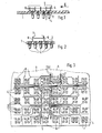
- the circuit board 1 for an area display or for a display board for information and illustration purposes has holes 2 in a predetermined grid, through which the connection legs 3 of light-emitting diodes 4 are inserted.
- On the opposite side of the LEDs 4 of the circuit board 1 driver or.
- Control modules 5 arranged at a distance above the circuit board surface.
- the connection pins 6 of the control or driver modules 5 stand up on the circuit board surface and are electrically and mechanically connected to the circuit board 1 by two parallel rows of soldering points 7.
- the light-emitting diodes 4 are also arranged continuously below the control or driver modules 5.
- the connecting legs 3 of the light-emitting diodes 4 are now electrically connected to the connecting pins 6 of the control or driver modules 5 via conductor tracks 8.
- the conductor pattern according to the invention clearly shows above all Figure 3.
- the nearest connecting legs 3 of light emitting diodes 4 are always connected to the connecting pins 6 of the driver modules 5. This takes place completely without taking into account the arrangement of the driver outputs inherent in the driver modules 5.
- the conductor tracks are usually made relatively short and without complicated guidance. Above all, the through-plating that is usually required at such high packing densities is eliminated.
- a printed circuit board 1 of an information display is equipped with groups of four LEDs 4 each in a square.
- the connection legs 3 of the light-emitting diodes 4 are inserted through the four pairs of bores and are mechanically and electrically connected to conductor tracks 8 on the back of the circuit board, which lead to connection points of the driver module (IC module) 5.
- a total of forty LEDs 4 are connected to a driver module 5 in this way.
- the connection points 7 for the driver module 5 are located in two mutually parallel rows between the connection points of the light-emitting diodes 4.
- the driver module 5 rises above the conductor tracks 8 and all connection points or soldering points, so that the geometric Arrangement is maintained throughout.
- the sensible conductor track routing permits relatively wide conductor tracks 8, as a result of which possible errors and interruptions, which often occur with very narrow conductor tracks, are avoided.
- the four light-emitting diodes in each group are switched through and connected to the driver module 5 with a short conductor track 8.
Landscapes
- Engineering & Computer Science (AREA)
- Microelectronics & Electronic Packaging (AREA)
- Devices For Indicating Variable Information By Combining Individual Elements (AREA)
- Physics & Mathematics (AREA)
- General Physics & Mathematics (AREA)
- Theoretical Computer Science (AREA)
- Control Of Indicators Other Than Cathode Ray Tubes (AREA)
- Cookers (AREA)
Priority Applications (1)
| Application Number | Priority Date | Filing Date | Title |
|---|---|---|---|
| AT87106227T ATE87164T1 (de) | 1986-05-30 | 1987-04-29 | Leiterplatte fuer flaechenanzeige. |
Applications Claiming Priority (2)
| Application Number | Priority Date | Filing Date | Title |
|---|---|---|---|
| DE3618285 | 1986-05-30 | ||
| DE3618285 | 1986-05-30 |
Publications (3)
| Publication Number | Publication Date |
|---|---|
| EP0247377A2 true EP0247377A2 (fr) | 1987-12-02 |
| EP0247377A3 EP0247377A3 (en) | 1989-10-11 |
| EP0247377B1 EP0247377B1 (fr) | 1993-03-17 |
Family
ID=6301996
Family Applications (1)
| Application Number | Title | Priority Date | Filing Date |
|---|---|---|---|
| EP87106227A Expired - Lifetime EP0247377B1 (fr) | 1986-05-30 | 1987-04-29 | Plaquette à circuit imprimé pour tableau d'indication |
Country Status (3)
| Country | Link |
|---|---|
| EP (1) | EP0247377B1 (fr) |
| AT (1) | ATE87164T1 (fr) |
| DE (1) | DE3784770D1 (fr) |
Cited By (3)
| Publication number | Priority date | Publication date | Assignee | Title |
|---|---|---|---|---|
| US5796376A (en) * | 1991-12-18 | 1998-08-18 | Cie Research, Inc. | Electronic display sign |
| FR2834112A1 (fr) * | 2001-12-24 | 2003-06-27 | Simon Elkrief | Dispositif de formation d'images par la commande de diodes electroluminescentes |
| FR2881017A1 (fr) * | 2005-01-17 | 2006-07-21 | Pierre Dumas | Circuit imprime fille a base 5 |
Family Cites Families (2)
| Publication number | Priority date | Publication date | Assignee | Title |
|---|---|---|---|---|
| BE789114A (fr) * | 1971-09-23 | 1973-03-22 | Int Standard Electric Corp | Perfectionnements aux methodes de conception assistee par ordinateur |
| FR2339922A1 (fr) * | 1976-01-28 | 1977-08-26 | Bourboulon Henri | Dispositif de signalisation lumineux |
-
1987
- 1987-04-29 AT AT87106227T patent/ATE87164T1/de not_active IP Right Cessation
- 1987-04-29 DE DE8787106227T patent/DE3784770D1/de not_active Expired - Lifetime
- 1987-04-29 EP EP87106227A patent/EP0247377B1/fr not_active Expired - Lifetime
Cited By (5)
| Publication number | Priority date | Publication date | Assignee | Title |
|---|---|---|---|---|
| US5796376A (en) * | 1991-12-18 | 1998-08-18 | Cie Research, Inc. | Electronic display sign |
| FR2834112A1 (fr) * | 2001-12-24 | 2003-06-27 | Simon Elkrief | Dispositif de formation d'images par la commande de diodes electroluminescentes |
| FR2881017A1 (fr) * | 2005-01-17 | 2006-07-21 | Pierre Dumas | Circuit imprime fille a base 5 |
| WO2006075108A3 (fr) * | 2005-01-17 | 2006-10-12 | Pierre-Alain Dumas | Circuit imprime pour 5 leds serie |
| US8246201B2 (en) | 2005-01-17 | 2012-08-21 | Pierre-Alain Dumas | Printed circuit for five LEDs in series |
Also Published As
| Publication number | Publication date |
|---|---|
| ATE87164T1 (de) | 1993-04-15 |
| EP0247377B1 (fr) | 1993-03-17 |
| DE3784770D1 (de) | 1993-04-22 |
| EP0247377A3 (en) | 1989-10-11 |
Similar Documents
| Publication | Publication Date | Title |
|---|---|---|
| DE10325550B4 (de) | Elektrisches Kontaktierungsverfahren | |
| CH667562A5 (de) | Verfahren zum aendern einer elektrischen flachbaugruppe. | |
| DE3447556A1 (de) | Multilayer-leiterverbindung | |
| DE3227959A1 (de) | Led-anzeige mit hohem informationsgehalt | |
| WO2008071541A2 (fr) | Module pour dispositif de contrôle destiné à tester des plaquettes de circuits imprimés | |
| EP0247377B1 (fr) | Plaquette à circuit imprimé pour tableau d'indication | |
| DE102007035065A1 (de) | Beleuchtungsvorrichtung | |
| DE8614663U1 (de) | Leiterplatte für Flächenanzeige | |
| WO2018184832A1 (fr) | Installation de distribution électrique et procédé pour traiter ou contrôler un arrangement d'appareils électriques ou électroniques d'une installation de distribution électrique | |
| DE1549683B1 (de) | Kodiergeraet zur erzeugung einer kodierten darstellung eines ausgewaehlten elementes einer matrix | |
| DE102008041697A1 (de) | Mehrdimensionale LED-Leiterplatte unter Verwendung von beabstandeten Platten | |
| DE102016118329A1 (de) | Steuergerät eines Kraftfahrzeugs | |
| DE2954194C2 (de) | Adapter zum Anschluß von eine Vielzahl von rasterartig verteilten Anschlußpunkten aufweisenden Prüflingen | |
| DE19752867B4 (de) | Optoelektronisches Anzeigemodul und Verfahren zu dessen Herstellung | |
| EP1083434A2 (fr) | Appareil pour tester des plaquettes de circuits imprimés | |
| DE2742135A1 (de) | Leiterplatine fuer die montage von integrierten schaltkreisen und/oder anderen bauelementen | |
| EP0538432A1 (fr) | Dispositif pour la realisation d'un circuit electrique, en particulier pour une sonde de mesure, et sonde de mesure. | |
| DE8424493U1 (de) | Prüfadapter | |
| DE2229784C2 (de) | Einrichtung zum Bestücken von Leiterplatten mit elektrischen bzw. elektronischen Bauelementen | |
| DE2631706B2 (de) | Bedientisch | |
| DE1946964A1 (de) | Beidseitig gedruckte Leiterplatte zum universellen Verschalten elektronischer Schaltungen mit integrierten Bausteinen | |
| DE2729834A1 (de) | Leiterplatte mit unterschiedlicher rasterteilung | |
| DE2304456A1 (de) | Einschubsystem fuer elektronikbaugruppen | |
| DE8411149U1 (de) | Baugruppe zur vereinfachung der montage von mehreren in einem messgeraet raeumlich getrennt anzuordnenden, elektrisch miteinander verknuepften leiterplatten | |
| DE8424847U1 (de) | Experimentier-Leiterplatte |
Legal Events
| Date | Code | Title | Description |
|---|---|---|---|
| PUAI | Public reference made under article 153(3) epc to a published international application that has entered the european phase |
Free format text: ORIGINAL CODE: 0009012 |
|
| AK | Designated contracting states |
Kind code of ref document: A2 Designated state(s): AT BE CH DE ES FR GB GR IT LI LU NL SE |
|
| PUAL | Search report despatched |
Free format text: ORIGINAL CODE: 0009013 |
|
| AK | Designated contracting states |
Kind code of ref document: A3 Designated state(s): AT BE CH DE ES FR GB GR IT LI LU NL SE |
|
| 17P | Request for examination filed |
Effective date: 19900327 |
|
| 17Q | First examination report despatched |
Effective date: 19911113 |
|
| GRAA | (expected) grant |
Free format text: ORIGINAL CODE: 0009210 |
|
| AK | Designated contracting states |
Kind code of ref document: B1 Designated state(s): AT BE CH DE ES FR GB GR IT LI LU NL SE |
|
| PG25 | Lapsed in a contracting state [announced via postgrant information from national office to epo] |
Ref country code: IT Free format text: LAPSE BECAUSE OF FAILURE TO SUBMIT A TRANSLATION OF THE DESCRIPTION OR TO PAY THE FEE WITHIN THE PRE;WARNING: LAPSES OF ITALIAN PATENTS WITH EFFECTIVE DATE BEFORE 2007 MAY HAVE OCCURRED AT ANY TIME BEFORE 2007. THE CORRECT EFFECTIVE DATE MAY BE DIFFERENT FROM THE ONE RECORDED.SCRIBED TIME-LIMIT Effective date: 19930317 Ref country code: SE Effective date: 19930317 Ref country code: NL Effective date: 19930317 Ref country code: FR Effective date: 19930317 Ref country code: GR Free format text: LAPSE BECAUSE OF FAILURE TO SUBMIT A TRANSLATION OF THE DESCRIPTION OR TO PAY THE FEE WITHIN THE PRESCRIBED TIME-LIMIT Effective date: 19930317 Ref country code: GB Effective date: 19930317 Ref country code: BE Effective date: 19930317 |
|
| REF | Corresponds to: |
Ref document number: 87164 Country of ref document: AT Date of ref document: 19930415 Kind code of ref document: T |
|
| REF | Corresponds to: |
Ref document number: 3784770 Country of ref document: DE Date of ref document: 19930422 |
|
| PG25 | Lapsed in a contracting state [announced via postgrant information from national office to epo] |
Ref country code: AT Effective date: 19930429 |
|
| PG25 | Lapsed in a contracting state [announced via postgrant information from national office to epo] |
Ref country code: LI Effective date: 19930430 Ref country code: LU Free format text: LAPSE BECAUSE OF NON-PAYMENT OF DUE FEES Effective date: 19930430 Ref country code: CH Effective date: 19930430 |
|
| PG25 | Lapsed in a contracting state [announced via postgrant information from national office to epo] |
Ref country code: ES Free format text: LAPSE BECAUSE OF FAILURE TO SUBMIT A TRANSLATION OF THE DESCRIPTION OR TO PAY THE FEE WITHIN THE PRESCRIBED TIME-LIMIT Effective date: 19930628 |
|
| EN | Fr: translation not filed | ||
| NLV1 | Nl: lapsed or annulled due to failure to fulfill the requirements of art. 29p and 29m of the patents act | ||
| GBV | Gb: ep patent (uk) treated as always having been void in accordance with gb section 77(7)/1977 [no translation filed] |
Effective date: 19930317 |
|
| REG | Reference to a national code |
Ref country code: CH Ref legal event code: PL |
|
| PLBE | No opposition filed within time limit |
Free format text: ORIGINAL CODE: 0009261 |
|
| STAA | Information on the status of an ep patent application or granted ep patent |
Free format text: STATUS: NO OPPOSITION FILED WITHIN TIME LIMIT |
|
| 26N | No opposition filed | ||
| PGFP | Annual fee paid to national office [announced via postgrant information from national office to epo] |
Ref country code: DE Payment date: 20060504 Year of fee payment: 20 |