EP0247503A2 - Méthode pour faire fonctionner un dispositif capteur d'images à état solide - Google Patents
Méthode pour faire fonctionner un dispositif capteur d'images à état solide Download PDFInfo
- Publication number
- EP0247503A2 EP0247503A2 EP87107292A EP87107292A EP0247503A2 EP 0247503 A2 EP0247503 A2 EP 0247503A2 EP 87107292 A EP87107292 A EP 87107292A EP 87107292 A EP87107292 A EP 87107292A EP 0247503 A2 EP0247503 A2 EP 0247503A2
- Authority
- EP
- European Patent Office
- Prior art keywords
- storage area
- charge storage
- conductivity type
- solid state
- state imager
- Prior art date
- Legal status (The legal status is an assumption and is not a legal conclusion. Google has not performed a legal analysis and makes no representation as to the accuracy of the status listed.)
- Granted
Links
Images

Classifications
-
- H—ELECTRICITY
- H10—SEMICONDUCTOR DEVICES; ELECTRIC SOLID-STATE DEVICES NOT OTHERWISE PROVIDED FOR
- H10F—INORGANIC SEMICONDUCTOR DEVICES SENSITIVE TO INFRARED RADIATION, LIGHT, ELECTROMAGNETIC RADIATION OF SHORTER WAVELENGTH OR CORPUSCULAR RADIATION
- H10F39/00—Integrated devices, or assemblies of multiple devices, comprising at least one element covered by group H10F30/00, e.g. radiation detectors comprising photodiode arrays
- H10F39/10—Integrated devices
- H10F39/12—Image sensors
- H10F39/15—Charge-coupled device [CCD] image sensors
- H10F39/153—Two-dimensional or three-dimensional array CCD image sensors
- H10F39/1534—Interline transfer
-
- H—ELECTRICITY
- H10—SEMICONDUCTOR DEVICES; ELECTRIC SOLID-STATE DEVICES NOT OTHERWISE PROVIDED FOR
- H10D—INORGANIC ELECTRIC SEMICONDUCTOR DEVICES
- H10D44/00—Charge transfer devices
- H10D44/40—Charge-coupled devices [CCD]
- H10D44/45—Charge-coupled devices [CCD] having field effect produced by insulated gate electrodes
- H10D44/462—Buried-channel CCD
Definitions
- This invention relates generally to a solid state imager device and is directed more particularly to an interline transfer type solid state imager device which has a light receiving section formed of a buried channel MOS structure.
- a conventional solid state imager device which can reduce the dark current, for example, is disclosed in a collection of papers presented at '84 National Conference of the Institute of Television Engineers of Japan, on pages 4l-42.
- Such known solid state imager device has a light receiving section which is formed of a buried channel MOS structure. Specifically, the device is constructed such that an n-type charge storage area is formed over the surface of a p-type silicon substrate and a forward electrode is formed on the charge storage area through an insulating layer, so that it can be operated under conditions where a hole storage layer is produced on a boundary between the n-type charge storage area and the insulating layer.
- the forward electrode is applied with a predetermined direct current voltage so as to form a channel within the n-type charge storage area from holes previously stored on the surface of the n-type charge storage area.
- the holes are kept in a so-called pinning state, so as to suppress the generation of hole-electron pairs which are the main component of the dark current from the surface level.
- a solid state imager device as described above can advantageously reduce the dark current.
- the present invention provides a solid state imager device comprising;
- FIGS. l-3 An embodiment of a solid state imager device according to the present invention will be described with reference to FIGS. l-3.
- FIG. l shows a p-type silicon substrate l into which a p-type impurity is diffused with a relatively low concentration. It is assumed in the present embodiment that a light receiving section 5, a vertical register section 6, a horizontal register section (not shown) and an output circuit section (not shown) are all formed on the p-type silicon substrate l. In the structure, a plurality of the light receiving sections 5 are provided which are arranged in the horizontal and vertical directions. The vertical register section 6 is arranged to be parallel to each of the vertically aligned light receiving sections 5, and the vertical register section 6 is arranged to be parallel to the horizontal register section, so as to form an interline transfer solid state imager device.
- the light receiving section 5 comprises an n-type charge storage area 2 on the surface of the p-type silicon substrate l.
- a forward electrode 4 is formed of a light transmissible polysilicon which is deposited over the charge storage area 2 through an insulating layer 3 made of SiO2, so that the light receiving section 5 is formed by the buried channel MOS structure.
- the forward electrode 4 When the solid state imager device of the present embodiment is operated so as to pick up an image, the forward electrode 4 is supplied through a terminal B with a pulse signal ⁇ v, as shown in FIG. 2A.
- a pulse signal ⁇ v When the forward electrode 4 is supplied with a low level voltage V1, e.g. -l2V, a storage layer of holes is formed on the boundary between the charge storage area 2 and the insulating layer 3, and when a high level voltage V2, e.g. 2V is supplied, the depletion layer beneath the charge storage area 2 is extended in the thickness direction of the substrate l.
- V1 low level voltage
- V2V high level voltage
- the pulse signal ⁇ v is selected such that its rising-up edge and its falling-down edge are within a horizontal blanking period so that the image signal is not influenced by the pulse signal ⁇ v.
- n-type overflow drain region 7 is formed adjacent to the charge storage area 2 through a p-type overflow control region 8 so as to prevent so-called blooming where the image picked up is made unclear by excessivee signal charges which are produced when an especially strong light is incident on the imager device, and which flow into other charge storage areas.
- a p-type channel stopper region 9 is arranged adjacent to the overflow drain region 7 as well as in regions between respective charge storage areas which are vertically adjacent to each other.
- the vertical register section 6 is formed of an n-type charge transfer region ll formed on a p-type well region l0 which is selectively formed on the p-type silicon substrate l and a transfer electrode l2 made of polysilicon is formed on the charge transfer region ll through the insulating layer 3.
- the vertical register section 6 is formed as a so-called bulk charge coupled device (BCCD) structure.
- FIG. l shows only one transfer electrode l2.
- the requried number of transfer electrodes l2 are provided so that the vertical register section 6 of the present embodiment is driven in a 4-phase driving manner.
- a gate electrode l3 for controlling the transfer of signal charges which accumulate in the charge storage area 2 to the charge transfer region ll in a manner such that it is integral with a portion of the transfer electrode l2, to thus form a gate section l4.
- the signal charges are transferred from the charge storage area 2 to the charge transfer region ll during a vertical flyback period using a low level voltage V1 which is supplied to the forward electrode 4.
- a light shielding layer l5 made e.g. of Al.
- a protective layer l6 made of SiO2.
- the forward electrode 4 is supplied with the pulse signal ⁇ v as shown in FIG. 2A.
- the forward electrode 4 is supplied with the low level voltage V1
- holes will accumulate on the surface of the charge storage area 2 and the the holes are kept in the pinning state, to suppress hole-electron pair generation from the surface level.
- the forward electrode 4 is supplied with the high level voltage V2
- the holes which have accumulated on the surface of the charge storage area 2 will be released.
- a dark signal such as shown in FIG. 2B will be generated in the charge storage area 2.
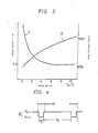
- a smear level value when the duty ratio T2/T1 is 0 is defined as l, and the curve illustrates variations in the smear level value as this ratio is varied.
- the present embodiment has advantages over the prior art in that the dark current and smear level can be effectively reduced by using a simple construction such that the forward electrode 4 is alternately supplied with the pulse signal ⁇ v consisting of a low level voltage V1, e.g. -l2V, for accumulating holes on the surface of the charge storage area 2 and a high level voltage V2, e.g. 2V, for extending the depletion layer beneath the charge storage area 2 and by using an appropriate duty ratio in the range of 2 - 5.
- V1 low level voltage
- V2V high level voltage
- a further advantage of the present embodiment is that the dark current from the surface level 8 is not completely suppressed but is produced in a degree such that the quality of the image is not influenced by the dark current which makes it difficult to distinguish minute local dark signals (white flaw), produced by crystal defects and the like and other factors than the surface level, which appear on an image if the dark current is completely suppressed.
- the low level voltage period T1 is determined as one horizontal period and the pulse signal ⁇ v raises and falls within the horizontal blanking period.
- a pulse signal ⁇ v ⁇ which has its low level voltage arranged within the horizontal blanking period, as shown in FIG. 4, may be applied to the forward electorde.
- the duty ratio T2/T1 can be set to have a sufficiently large value so that smear can be satisfactorily suppressed, and so that the surface is not depleted continuously for more than one horizontal period so that the dark current can also be sufficiently suppressed.
- the above described present embodiment is for the case where the signal charges are electrons.
- the present invention may be applied to a case where the signal charges are holes.
- the conductivity types of the respective sections are selected so as to opposite to those shown in FIG. l. The same effects as described above can be obtained in this case.
Landscapes
- Solid State Image Pick-Up Elements (AREA)
- Transforming Light Signals Into Electric Signals (AREA)
Applications Claiming Priority (2)
| Application Number | Priority Date | Filing Date | Title |
|---|---|---|---|
| JP61114375A JPS62269357A (ja) | 1986-05-19 | 1986-05-19 | 固体撮像装置 |
| JP114375/86 | 1986-05-19 |
Publications (3)
| Publication Number | Publication Date |
|---|---|
| EP0247503A2 true EP0247503A2 (fr) | 1987-12-02 |
| EP0247503A3 EP0247503A3 (en) | 1990-04-04 |
| EP0247503B1 EP0247503B1 (fr) | 1995-03-01 |
Family
ID=14636115
Family Applications (1)
| Application Number | Title | Priority Date | Filing Date |
|---|---|---|---|
| EP87107292A Expired - Lifetime EP0247503B1 (fr) | 1986-05-19 | 1987-05-19 | Méthode pour faire fonctionner un dispositif capteur d'images à état solide |
Country Status (5)
| Country | Link |
|---|---|
| US (1) | US4794279A (fr) |
| EP (1) | EP0247503B1 (fr) |
| JP (1) | JPS62269357A (fr) |
| KR (1) | KR960004467B1 (fr) |
| DE (1) | DE3751102T2 (fr) |
Cited By (2)
| Publication number | Priority date | Publication date | Assignee | Title |
|---|---|---|---|---|
| EP0399601A1 (fr) * | 1989-05-23 | 1990-11-28 | Koninklijke Philips Electronics N.V. | Réduction du courant d'obscurité dans un dispositif capteur d'images à couplage de charges à canal enterré |
| EP0332173A3 (fr) * | 1988-03-08 | 1991-03-06 | Kabushiki Kaisha Toshiba | Dispositif capteur d'images à l'état solide |
Families Citing this family (14)
| Publication number | Priority date | Publication date | Assignee | Title |
|---|---|---|---|---|
| JPH01125074A (ja) * | 1987-11-10 | 1989-05-17 | Fuji Photo Film Co Ltd | 固体撮像装置 |
| JPH0766961B2 (ja) * | 1988-10-07 | 1995-07-19 | 三菱電機株式会社 | 固体撮像素子 |
| JPH02309877A (ja) * | 1989-05-25 | 1990-12-25 | Sony Corp | 固体撮像装置 |
| US5528643A (en) * | 1989-11-13 | 1996-06-18 | Texas Instruments Incorporated | Charge coupled device/charge super sweep image system and method for making |
| US5182623A (en) * | 1989-11-13 | 1993-01-26 | Texas Instruments Incorporated | Charge coupled device/charge super sweep image system and method for making |
| JP2738589B2 (ja) * | 1990-09-05 | 1998-04-08 | 三菱電機株式会社 | 固体撮像素子 |
| JP2690612B2 (ja) * | 1990-10-05 | 1997-12-10 | キヤノン株式会社 | 光電変換装置 |
| US5329149A (en) * | 1990-10-12 | 1994-07-12 | Seiko Instruments Inc. | Image sensor with non-light-transmissive layer having photosensing windows |
| JP2500428B2 (ja) * | 1993-04-06 | 1996-05-29 | 日本電気株式会社 | イメ―ジセンサおよびその駆動方法 |
| US5757427A (en) * | 1993-04-23 | 1998-05-26 | Hamamatsu Photonics K.K. | Image pick-up apparatus having a charge coupled device with multiple electrodes, a buffer layer located below some of the electrodes |
| JPH08264747A (ja) * | 1995-03-16 | 1996-10-11 | Eastman Kodak Co | コンテナ側方オーバーフロードレインインプラントを有する固体画像化器及びその製造方法 |
| JP2005348061A (ja) * | 2004-06-02 | 2005-12-15 | Sanyo Electric Co Ltd | 電子カメラ |
| EP1608019B1 (fr) * | 2004-06-15 | 2010-02-24 | STMicroelectronics (Research & Development) Limited | Capteur d'image |
| EP2487714B1 (fr) * | 2009-10-09 | 2018-12-05 | National University Corporation Shizuoka University | Élément semi-conducteur et dispositif à l'état solide de capture d'images |
Family Cites Families (5)
| Publication number | Priority date | Publication date | Assignee | Title |
|---|---|---|---|---|
| JPS5323224A (en) * | 1976-08-16 | 1978-03-03 | Hitachi Ltd | Solid pickup unit |
| JPS6157181A (ja) * | 1984-08-28 | 1986-03-24 | Sharp Corp | 固体撮像装置 |
| US4743778A (en) * | 1985-03-25 | 1988-05-10 | Nippon Kogaku K. K. | Solid-state area imaging device having interline transfer CCD |
| JPH0795827B2 (ja) * | 1985-07-22 | 1995-10-11 | 株式会社ニコン | カメラ駆動装置 |
| JPS61219271A (ja) * | 1985-03-25 | 1986-09-29 | Nippon Kogaku Kk <Nikon> | インタ−ライン転送型ccdの駆動方法 |
-
1986
- 1986-05-19 JP JP61114375A patent/JPS62269357A/ja active Pending
-
1987
- 1987-05-18 US US07/050,400 patent/US4794279A/en not_active Expired - Lifetime
- 1987-05-18 KR KR1019870004874A patent/KR960004467B1/ko not_active Expired - Fee Related
- 1987-05-19 DE DE3751102T patent/DE3751102T2/de not_active Expired - Fee Related
- 1987-05-19 EP EP87107292A patent/EP0247503B1/fr not_active Expired - Lifetime
Cited By (2)
| Publication number | Priority date | Publication date | Assignee | Title |
|---|---|---|---|---|
| EP0332173A3 (fr) * | 1988-03-08 | 1991-03-06 | Kabushiki Kaisha Toshiba | Dispositif capteur d'images à l'état solide |
| EP0399601A1 (fr) * | 1989-05-23 | 1990-11-28 | Koninklijke Philips Electronics N.V. | Réduction du courant d'obscurité dans un dispositif capteur d'images à couplage de charges à canal enterré |
Also Published As
| Publication number | Publication date |
|---|---|
| JPS62269357A (ja) | 1987-11-21 |
| EP0247503B1 (fr) | 1995-03-01 |
| KR960004467B1 (ko) | 1996-04-06 |
| EP0247503A3 (en) | 1990-04-04 |
| KR880014678A (ko) | 1988-12-24 |
| DE3751102D1 (de) | 1995-04-06 |
| US4794279A (en) | 1988-12-27 |
| DE3751102T2 (de) | 1995-10-12 |
Similar Documents
| Publication | Publication Date | Title |
|---|---|---|
| US4484210A (en) | Solid-state imaging device having a reduced image lag | |
| US4774586A (en) | Interline type charge transfer imaging device | |
| US4322753A (en) | Smear and/or blooming in a solid state charge transfer image pickup device | |
| US4717945A (en) | Solid state image pick-up device with a shutter function | |
| EP0247503B1 (fr) | Méthode pour faire fonctionner un dispositif capteur d'images à état solide | |
| US5962882A (en) | Charge coupled devices including buried transmission gates | |
| US4851890A (en) | Solid-state image sensor | |
| US4242599A (en) | Charge transfer image sensor with antiblooming and exposure control | |
| US4485315A (en) | Blooming suppression in a CCD imaging device | |
| US4672455A (en) | Solid-state image-sensor having reverse-biased substrate and transfer registers | |
| US4462047A (en) | Solid state imager with blooming suppression | |
| CA1193711A (fr) | Senseur d'images a semiconducteurs | |
| JPS6262553A (ja) | 固体撮像装置 | |
| US5402459A (en) | Frame transfer image sensor with electronic shutter | |
| US5426317A (en) | Frame interline transfer CCD imager | |
| GB2128052A (en) | Flicker reduction in field-interlaced three-phase clocked ccd imagers | |
| US4584697A (en) | Four-phase charge-coupled device having an oversized electrode | |
| US5760430A (en) | Charge transfer device and solid-state imaging apparatus using the same device | |
| US6891243B2 (en) | Solid-state image pick-up device | |
| EP0499275A1 (fr) | Capteur d'images à état solide | |
| KR101293586B1 (ko) | 고체촬상장치 및 고체촬상장치의 구동방법 | |
| US4837629A (en) | Image pickup method using a CCD-type solid state image pickup device with charge dissipation | |
| US5907356A (en) | Solid-state image pickup device | |
| JP2002151673A (ja) | 固体撮像素子 | |
| JPS60244068A (ja) | 埋込みチヤネル電荷結合素子 |
Legal Events
| Date | Code | Title | Description |
|---|---|---|---|
| PUAI | Public reference made under article 153(3) epc to a published international application that has entered the european phase |
Free format text: ORIGINAL CODE: 0009012 |
|
| AK | Designated contracting states |
Kind code of ref document: A2 Designated state(s): DE FR GB NL |
|
| PUAL | Search report despatched |
Free format text: ORIGINAL CODE: 0009013 |
|
| AK | Designated contracting states |
Kind code of ref document: A3 Designated state(s): DE FR GB NL |
|
| 17P | Request for examination filed |
Effective date: 19900927 |
|
| 17Q | First examination report despatched |
Effective date: 19920515 |
|
| GRAA | (expected) grant |
Free format text: ORIGINAL CODE: 0009210 |
|
| AK | Designated contracting states |
Kind code of ref document: B1 Designated state(s): DE FR GB NL |
|
| REF | Corresponds to: |
Ref document number: 3751102 Country of ref document: DE Date of ref document: 19950406 |
|
| ET | Fr: translation filed | ||
| PLBE | No opposition filed within time limit |
Free format text: ORIGINAL CODE: 0009261 |
|
| STAA | Information on the status of an ep patent application or granted ep patent |
Free format text: STATUS: NO OPPOSITION FILED WITHIN TIME LIMIT |
|
| 26N | No opposition filed | ||
| REG | Reference to a national code |
Ref country code: GB Ref legal event code: IF02 |
|
| PGFP | Annual fee paid to national office [announced via postgrant information from national office to epo] |
Ref country code: FR Payment date: 20030508 Year of fee payment: 17 |
|
| PGFP | Annual fee paid to national office [announced via postgrant information from national office to epo] |
Ref country code: GB Payment date: 20030514 Year of fee payment: 17 |
|
| PGFP | Annual fee paid to national office [announced via postgrant information from national office to epo] |
Ref country code: DE Payment date: 20030529 Year of fee payment: 17 |
|
| PGFP | Annual fee paid to national office [announced via postgrant information from national office to epo] |
Ref country code: NL Payment date: 20030530 Year of fee payment: 17 |
|
| PG25 | Lapsed in a contracting state [announced via postgrant information from national office to epo] |
Ref country code: GB Free format text: LAPSE BECAUSE OF NON-PAYMENT OF DUE FEES Effective date: 20040519 |
|
| PG25 | Lapsed in a contracting state [announced via postgrant information from national office to epo] |
Ref country code: NL Free format text: LAPSE BECAUSE OF NON-PAYMENT OF DUE FEES Effective date: 20041201 Ref country code: DE Free format text: LAPSE BECAUSE OF NON-PAYMENT OF DUE FEES Effective date: 20041201 |
|
| GBPC | Gb: european patent ceased through non-payment of renewal fee |
Effective date: 20040519 |
|
| PG25 | Lapsed in a contracting state [announced via postgrant information from national office to epo] |
Ref country code: FR Free format text: LAPSE BECAUSE OF NON-PAYMENT OF DUE FEES Effective date: 20050131 |
|
| NLV4 | Nl: lapsed or anulled due to non-payment of the annual fee |
Effective date: 20041201 |
|
| REG | Reference to a national code |
Ref country code: FR Ref legal event code: ST |