EP0247834A1 - Régénérateur pour signaux optiques - Google Patents
Régénérateur pour signaux optiques Download PDFInfo
- Publication number
- EP0247834A1 EP0247834A1 EP87304657A EP87304657A EP0247834A1 EP 0247834 A1 EP0247834 A1 EP 0247834A1 EP 87304657 A EP87304657 A EP 87304657A EP 87304657 A EP87304657 A EP 87304657A EP 0247834 A1 EP0247834 A1 EP 0247834A1
- Authority
- EP
- European Patent Office
- Prior art keywords
- optical
- amplifier
- signal
- input
- output
- Prior art date
- Legal status (The legal status is an assumption and is not a legal conclusion. Google has not performed a legal analysis and makes no representation as to the accuracy of the status listed.)
- Granted
Links
Images


Classifications
-
- H—ELECTRICITY
- H04—ELECTRIC COMMUNICATION TECHNIQUE
- H04B—TRANSMISSION
- H04B10/00—Transmission systems employing electromagnetic waves other than radio-waves, e.g. infrared, visible or ultraviolet light, or employing corpuscular radiation, e.g. quantum communication
- H04B10/29—Repeaters
- H04B10/291—Repeaters in which processing or amplification is carried out without conversion of the main signal from optical form
- H04B10/299—Signal waveform processing, e.g. reshaping or retiming
-
- H—ELECTRICITY
- H01—ELECTRIC ELEMENTS
- H01S—DEVICES USING THE PROCESS OF LIGHT AMPLIFICATION BY STIMULATED EMISSION OF RADIATION [LASER] TO AMPLIFY OR GENERATE LIGHT; DEVICES USING STIMULATED EMISSION OF ELECTROMAGNETIC RADIATION IN WAVE RANGES OTHER THAN OPTICAL
- H01S5/00—Semiconductor lasers
- H01S5/50—Amplifier structures not provided for in groups H01S5/02 - H01S5/30
-
- H—ELECTRICITY
- H04—ELECTRIC COMMUNICATION TECHNIQUE
- H04B—TRANSMISSION
- H04B10/00—Transmission systems employing electromagnetic waves other than radio-waves, e.g. infrared, visible or ultraviolet light, or employing corpuscular radiation, e.g. quantum communication
- H04B10/29—Repeaters
- H04B10/291—Repeaters in which processing or amplification is carried out without conversion of the main signal from optical form
- H04B10/2912—Repeaters in which processing or amplification is carried out without conversion of the main signal from optical form characterised by the medium used for amplification or processing
- H04B10/2914—Repeaters in which processing or amplification is carried out without conversion of the main signal from optical form characterised by the medium used for amplification or processing using lumped semiconductor optical amplifiers [SOA]
-
- H—ELECTRICITY
- H04—ELECTRIC COMMUNICATION TECHNIQUE
- H04L—TRANSMISSION OF DIGITAL INFORMATION, e.g. TELEGRAPHIC COMMUNICATION
- H04L7/00—Arrangements for synchronising receiver with transmitter
- H04L7/0075—Arrangements for synchronising receiver with transmitter with photonic or optical means
-
- H—ELECTRICITY
- H04—ELECTRIC COMMUNICATION TECHNIQUE
- H04L—TRANSMISSION OF DIGITAL INFORMATION, e.g. TELEGRAPHIC COMMUNICATION
- H04L7/00—Arrangements for synchronising receiver with transmitter
- H04L7/02—Speed or phase control by the received code signals, the signals containing no special synchronisation information
- H04L7/027—Speed or phase control by the received code signals, the signals containing no special synchronisation information extracting the synchronising or clock signal from the received signal spectrum, e.g. by using a resonant or bandpass circuit
-
- H—ELECTRICITY
- H01—ELECTRIC ELEMENTS
- H01S—DEVICES USING THE PROCESS OF LIGHT AMPLIFICATION BY STIMULATED EMISSION OF RADIATION [LASER] TO AMPLIFY OR GENERATE LIGHT; DEVICES USING STIMULATED EMISSION OF ELECTROMAGNETIC RADIATION IN WAVE RANGES OTHER THAN OPTICAL
- H01S5/00—Semiconductor lasers
- H01S5/06—Arrangements for controlling the laser output parameters, e.g. by operating on the active medium
- H01S5/0607—Arrangements for controlling the laser output parameters, e.g. by operating on the active medium by varying physical parameters other than the potential of the electrodes, e.g. by an electric or magnetic field, mechanical deformation, pressure, light, temperature
- H01S5/0608—Arrangements for controlling the laser output parameters, e.g. by operating on the active medium by varying physical parameters other than the potential of the electrodes, e.g. by an electric or magnetic field, mechanical deformation, pressure, light, temperature controlled by light, e.g. optical switch
Definitions
- optical is intended to refer to the visible region of the electromagnetic spectrum together with those parts of the infrared and ultraviolet regions at each end of the visible region which are capable of being transmitted by dielectric optical waveguides such as optical fibres.
- an optical signal regenerator comprises an optical coupler having a first input for an optical information signal, a second input for optical clock pulses and an output for a combined signal, and a resonant laser amplifier downstream of the output of the coupler and arranged to receive the combined signal and, in use, output a regenerated optical information signal.
- the bias current applied to the laser amplifier biases the amplifier to a level below its lasing threshold, and the power of the optical clock pulses is just below the bistable threshold of the amplifier, so that, when an optical information signal is fed into the first input during the application of an optical clock pulse to the second input, the bistable threshold of the amplifier is exceeded causing a sudden jump in the power of the optical output of the amplifier to provide a regenerated optical information signal.
- the lasing threshold and the bistable threshold apply to distinct phenomena.
- the electrical bias applied to the laser amplifier is below the lasing threshold bias current and consequently the amplifier does not lase.
- the sudden amplification occurs because the optical power of an input optical signal is made to exceed an optical power bistable threshold for the amplifier.
- the optical power input to a semiconductor laser amplifier When the optical power input to a semiconductor laser amplifier is increased, the extra stimulated emission raises the recombination rate. The carrier density is correspondingly reduced. As a result, the effective refractive index of the active region of a resonant laser amplifier increases with the optical power passing through it. The amplifier resonances are thereby tuned to longer wavelengths, and the gain at a given wavelength therefore varies. The power transfer characteristics of such an amplifier are consequently non-linear and, at appropriate input wavelengths, bistable operation is made possible.
- Regeneration is achieved by combining an input signal with an optical clock signal and coupling them both into the resonant optical amplifier.
- the clock signal consists of a train of optical pulses at the desired regeneration rate and with a wavelength at which the amplifier is bistable.
- the peak power of the clock signal is held marginally below the bistable threshold optical power level at which the amplifier will jump into a higher gain state.
- the output of the amplifier With a low level input signal the output of the amplifier is in a lower gain state and its output comprises the slightly amplified clock signal.
- the input signal increases to a high enough level such that the extra power in the combined input and clock signals is sufficient to exceed the bistable threshold then suddenly the resonant wavelength of the laser amplifier is matched to that of the light passing through it and the amplifier jumps into the higher gain state. It remains in this state, even if the input signal level again falls, until the end of the current clock pulse.
- the output of the amplifier for that period then includes a highly amplified clock pulse.
- the complete regenerated signal comprises a train of return-to-zero pulses with the timing and wavelength of the clock signal.
- the input signal need not be at the same wavelength as the clock signal, so long as the amplifier has adequate gain at the input signal wavelength to trigger the bistable operation. Therefore, for example, the wavelength may be shifted between input and output by multiples of the amplifier mode spacing.
- the optical signal regenerator may include an optical clock pulse generator which generates optical clock pulses in synchronism with a standard clock such as a system clock or, alternatively, it may be arranged to recover timing information from the input optical information signal and generate the clock pulses in accordance with this recovered timing information.
- a standard clock such as a system clock
- the optical signal regenerator may also include biasing means such as a constant current source to provide a bias current which biases the laser amplifier to a level just below its lasing threshold.
- biasing means such as a constant current source to provide a bias current which biases the laser amplifier to a level just below its lasing threshold.
- the regenerator includes an optical clock pulse generator preferably it also includes power control means which control the power of the optical clock pulses to a level just below the bistable threshold of the laser amplifier.
- the control means may monitor the output of the laser amplifier at a time that the regenerated output signal is not being emitted and control the power of the clock pulses in accordance with the monitored output.
- the resonant laser amplifier is preferably formed by a semiconductor laser amplifier and this may have the form of a resonant Fabry-Perot amplifier or a distributed feedback laser.
- the clock pulses do not have the same wavelength as the input optical information signal and preferably the clock pulses have a wavelength slightly longer than that of the input information signal.
- the clock pulses may be removed from the input information signal by multiples of the mode spacing in either direction when the laser amplifier is of the Fabry-Perot type.
- the clock pulses would be of the order of ten or tens of nanometers longer or shorter than that of the input information signal.
- the regenerator can be used as a wavelength shifter.
- Filtering means such as a monochromator or narrow bandpass filter may be located downstream of the resonant laser amplifier to separate the regenerated information signal from the slightly amplified input information signal and any spontaneous emission generated by the laser. However, filtering means are unnecessary when equipment which receives the regenerated information signal downstream from the laser is only responsive to light of the regenerated signal wavelength.
- the illustrated optical signal regenerator in accordance with this invention includes an optical coupler 1 having an optical signal input 2, a clock pulse input 3 and an output 4 for the combined signal, and a laser amplifier 5 coupled to receive the combined signal from the output 4.
- the laser amplifier 5 is a double channel planar buried heterostructure semiconductor laser such as that described in an article in Electronics Letters 23 May 1985, Vol.21, No.11, pages 493-494, entitled "High Performance DC-PBH Lasers at 1.52 micrometres by a Hybrid MOVPE/LPE Process", by Nelson A W, Wong S, Regnault J C, Hobbs R E, Murrel D L, and Walling R H.
- the facet reflectivies of the laser are reduced to 3% by the application of anti-reflection coating.
- an input signal to the first input 2 is produced by a distributed feedback laser 7 having a wavelength of 1526 nm which is driven from a 140 Mb/second pattern generator 8.
- the pattern generator 8 is also used to drive a clock source formed by an external cavity tuneable laser 9 having a wavelength of 1514 nm.
- the output of the laser amplifier 5 passes through an optical bandpass filter 10 centred on 1514 nm and the output from this is received by a photodiode 11 connected to an input of an oscilloscope 12.
- the combined optical signal input to the amplifier can be monitored at the output 13 of the coupler 1 using a receiver and oscilloscope arrangement analogous to that illustrated for monitoring the amplifier output. Alternatively the output 13 may be conventionally terminated in a non-reflecting manner.
- Figure 1 shows typical theoretical characteristics of the amplifier 5 for light input of four different wavelengths A, B, C, D at 0, 0.1, 0.15 and 0.2 nm longer respectively than a resonant wavelength for the amplifier at zero input power.
- the characteristic curve is generally S-shaped. In this case, where the input wavelength exceeds the zero power resonance by 0.1nm or less, as shown by curves A and B, the characteristic is not bistable.
- the S-shaped curves C and D illustrate the bistable nature of the laser amplifier when the input wavelength is slightly longer.
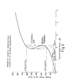
- Figure 2 shows one such curve. From this Figure, it is clear that if the power of the clock signals passing through the laser 5 is arranged to be close to the bistable threshold then a slight increase in the optical power, for example that provided by the optical information in an input optical signal, is just sufficient to exceed the bistable threshold. This results in an immediate jump in output power of the amplifier to the upper part of the curve shown in Figure 2. During any subsequent reduction of the optical input information signal the output power returns along the upper part of the curve. The regenerated output signal therefore remains high for the remainder of the duration of the clock pulse irrespective of a subsequent fall in the optical information signal.
- the output of the amplifier follows the hysteresis loop shown in Figure 2 moving between the high and low amplification levels to provide a regenerated signal which consists of large and small pulses at the clock frequency corresponding to "ones" and "zeroes" in the input signal.
- the low level amplification of the clock signal during the input signal lows therefore means that the extinction ratio is finite.
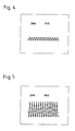
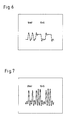
- FIG 4 illustrates a typical optical data stream input to the amplifier when the distributed feedback laser 7 is modulated by the pattern generator 8 with a non-return-to-zero data stream at 140 mb/second.
- the corresponding output of the laser amplifier 5 is a regenerated pattern in a return-to-zero form at 1514 nm as shown in Figure 7.
Landscapes
- Physics & Mathematics (AREA)
- Computer Networks & Wireless Communication (AREA)
- Signal Processing (AREA)
- Engineering & Computer Science (AREA)
- Electromagnetism (AREA)
- Optics & Photonics (AREA)
- Condensed Matter Physics & Semiconductors (AREA)
- General Physics & Mathematics (AREA)
- Semiconductor Lasers (AREA)
- Optical Communication System (AREA)
- Holo Graphy (AREA)
- Silicon Polymers (AREA)
- Lasers (AREA)
- Developing Agents For Electrophotography (AREA)
- Pyrane Compounds (AREA)
- Light Guides In General And Applications Therefor (AREA)
Priority Applications (1)
| Application Number | Priority Date | Filing Date | Title |
|---|---|---|---|
| AT87304657T ATE83346T1 (de) | 1986-05-28 | 1987-05-26 | Optischer signalregenerator. |
Applications Claiming Priority (2)
| Application Number | Priority Date | Filing Date | Title |
|---|---|---|---|
| GB8612956 | 1986-05-28 | ||
| GB868612956A GB8612956D0 (en) | 1986-05-28 | 1986-05-28 | Optical signal regenerator |
Publications (2)
| Publication Number | Publication Date |
|---|---|
| EP0247834A1 true EP0247834A1 (fr) | 1987-12-02 |
| EP0247834B1 EP0247834B1 (fr) | 1992-12-09 |
Family
ID=10598558
Family Applications (1)
| Application Number | Title | Priority Date | Filing Date |
|---|---|---|---|
| EP87304657A Expired - Lifetime EP0247834B1 (fr) | 1986-05-28 | 1987-05-26 | Régénérateur pour signaux optiques |
Country Status (9)
| Country | Link |
|---|---|
| US (1) | US4879761A (fr) |
| EP (1) | EP0247834B1 (fr) |
| JP (1) | JPH0683143B2 (fr) |
| AT (1) | ATE83346T1 (fr) |
| CA (1) | CA1282831C (fr) |
| DE (1) | DE3782974T2 (fr) |
| ES (1) | ES2036574T3 (fr) |
| GB (1) | GB8612956D0 (fr) |
| WO (1) | WO1987007458A1 (fr) |
Cited By (4)
| Publication number | Priority date | Publication date | Assignee | Title |
|---|---|---|---|---|
| EP0386736A1 (fr) * | 1989-03-09 | 1990-09-12 | Canon Kabushiki Kaisha | Système de communication optique |
| WO1991017474A1 (fr) * | 1990-05-08 | 1991-11-14 | British Telecommunications Public Limited Company | Regenerateur de signal optique et systeme de communication optique l'incorporant |
| DE4038503A1 (de) * | 1990-12-03 | 1992-06-04 | Kommunikations Elektronik | Vorrichtung zum verbinden von zwei optischen fasern |
| NL1004806C2 (nl) * | 1996-12-17 | 1998-06-18 | Nederland Ptt | Optische lange-afstands signaaltransmissie met optische versterking. |
Families Citing this family (19)
| Publication number | Priority date | Publication date | Assignee | Title |
|---|---|---|---|---|
| GB8709073D0 (en) * | 1987-04-15 | 1987-05-20 | British Telecomm | Coherent optical systems |
| ES2070901T3 (es) * | 1988-01-22 | 1995-06-16 | At & T Corp | Comunicacion optica por sincronizacion por inyeccion con una señal que modula una portadora optica. |
| US5073981A (en) * | 1988-01-22 | 1991-12-17 | At&T Bell Laboratories | Optical communication by injection-locking to a signal which modulates an optical carrier |
| IT1219324B (it) * | 1988-05-24 | 1990-05-03 | Cselt Centro Studi Lab Telecom | Procedimento per la caratterizzazione di laser a semiconduttore ristabili |
| US5119039A (en) * | 1990-12-31 | 1992-06-02 | Gte Laboratories Incorporated | Semiconductor optical amplifier with wideband electrical response |
| CA2068975C (fr) * | 1991-05-20 | 2002-03-26 | Kazunori Nakamura | Systeme d'amplification optique |
| US5194979A (en) * | 1991-06-07 | 1993-03-16 | Gte Laboratories Incorporated | Wideband optical amplifier-receiver system |
| US5264960A (en) * | 1992-05-08 | 1993-11-23 | At&T Bell Laboratories | Optical wavelength shifter |
| JPH05347449A (ja) * | 1992-06-12 | 1993-12-27 | Ando Electric Co Ltd | 信号光及び信号光と波長の違う連続光を増幅する光増幅器 |
| US5359450A (en) * | 1992-06-25 | 1994-10-25 | Synchronous Communications, Inc. | Optical transmission system |
| US5535968A (en) * | 1992-07-27 | 1996-07-16 | Union Switch & Signal Inc. | Vital railway signal link |
| US5463488A (en) * | 1992-07-31 | 1995-10-31 | At&T Ipm Corp. | Distribution of clock signals by pump power modulation in an optically amplified network |
| US5532863A (en) * | 1994-07-27 | 1996-07-02 | U.S. Philips Corporation | Optical signal-regenerating unit and transmission system comprising such a unit |
| EP0717482A1 (fr) * | 1994-12-14 | 1996-06-19 | AT&T Corp. | Dispositif optique interférometrique à semi-conducteur pour la conversion de longueur d'onde |
| US5880866A (en) * | 1996-11-13 | 1999-03-09 | At&T Corp | Time division demultiplexing using selective Raman amplification |
| US6463113B1 (en) * | 1997-06-05 | 2002-10-08 | Compaq Information Technologies Group, L.P. | External signal attenuator for a single-ended transmission line |
| JP4689008B2 (ja) | 2000-07-04 | 2011-05-25 | 富士通株式会社 | 信号光を波形整形するための方法及び装置 |
| US20040066550A1 (en) * | 2002-10-02 | 2004-04-08 | Jay Paul R. | Optical pulse reshaping system |
| US7375812B2 (en) * | 2005-02-22 | 2008-05-20 | Axsun Technologies, Inc. | Method and system for reducing parasitic spectral noise in tunable semiconductor source spectroscopy system |
Citations (3)
| Publication number | Priority date | Publication date | Assignee | Title |
|---|---|---|---|---|
| DE2248211A1 (de) * | 1972-10-02 | 1974-04-11 | Allg Elek Citaets Ges Aeg Tele | Faserleitungs-nachrichtenuebertragungssystem |
| US3887876A (en) * | 1972-10-03 | 1975-06-03 | Siemens Ag | Optical intermediate amplifier for a communication system |
| EP0143561A2 (fr) * | 1983-11-25 | 1985-06-05 | The Board Of Trustees Of The Leland Stanford Junior University | Amplificateur optique comprenant une fibre optique |
Family Cites Families (5)
| Publication number | Priority date | Publication date | Assignee | Title |
|---|---|---|---|---|
| DE2418981B2 (de) * | 1974-04-19 | 1976-10-28 | Max-Planck-Gesellschaft zur Förderung der Wissenschaften e.V., 3400 Göttingen | Verfahren und einrichtung zur optischen doppelanregung eines stimulierbaren mediums zum verringern der zeitlichen schwankungen der laserpulse im pulsbetrieb mit passiv phasengekoppelter gueteschaltung |
| US4475201A (en) * | 1981-06-11 | 1984-10-02 | Photochemical Research Associates Inc. | Longitudinally pumped dye laser arrangement |
| EP0110388B1 (fr) * | 1982-11-29 | 1987-10-07 | Nec Corporation | Système de commutation optique à division temporelle utilisant des dispositifs optiques bistables |
| US4562582A (en) * | 1983-04-18 | 1985-12-31 | Nippon Telegraph & Telephone Public Corporation | Burst signal receiving apparatus |
| JPH0632332B2 (ja) * | 1984-08-24 | 1994-04-27 | 日本電気株式会社 | 半導体レ−ザ装置 |
-
1986
- 1986-05-28 GB GB868612956A patent/GB8612956D0/en active Pending
-
1987
- 1987-05-26 WO PCT/GB1987/000360 patent/WO1987007458A1/fr not_active Ceased
- 1987-05-26 JP JP62503119A patent/JPH0683143B2/ja not_active Expired - Lifetime
- 1987-05-26 DE DE8787304657T patent/DE3782974T2/de not_active Expired - Lifetime
- 1987-05-26 EP EP87304657A patent/EP0247834B1/fr not_active Expired - Lifetime
- 1987-05-26 ES ES198787304657T patent/ES2036574T3/es not_active Expired - Lifetime
- 1987-05-26 US US07/143,857 patent/US4879761A/en not_active Expired - Lifetime
- 1987-05-26 AT AT87304657T patent/ATE83346T1/de not_active IP Right Cessation
- 1987-05-27 CA CA000538088A patent/CA1282831C/fr not_active Expired - Lifetime
Patent Citations (3)
| Publication number | Priority date | Publication date | Assignee | Title |
|---|---|---|---|---|
| DE2248211A1 (de) * | 1972-10-02 | 1974-04-11 | Allg Elek Citaets Ges Aeg Tele | Faserleitungs-nachrichtenuebertragungssystem |
| US3887876A (en) * | 1972-10-03 | 1975-06-03 | Siemens Ag | Optical intermediate amplifier for a communication system |
| EP0143561A2 (fr) * | 1983-11-25 | 1985-06-05 | The Board Of Trustees Of The Leland Stanford Junior University | Amplificateur optique comprenant une fibre optique |
Non-Patent Citations (4)
| Title |
|---|
| 1973 IEEE/OSA CONFERENCE ON LASER ENGINEERING AND APPLICATIONS, Washington, D.C., 30th May - 1st June 1973, page 24, IEEE, New York, US; D. SCHICKETANZ et al.: "Optical repeater for a wide-band fiber communication system" * |
| ELECTRONICS LETTERS, vol. 21, no. 11, 23rd May 1985, pages 501-502, Stevenage, Herts, GB; M.J. O'MAHONY et al.: "Low-reflectivity semiconductor laser amplifier with 20 dB fibre-to-fibre gain at 1500 nm" * |
| IEEE SPECTRUM, vol. 21, no. 5, May 1984, pages 26-33, IEEE, New York, US; S. KOBAYASHI et al.: "Semiconductor optical amplifiers" * |
| PATENT ABSTRACTS OF JAPAN, vol. 4, no. 87, 21st June 1980, page 569 E 16; & JP-A-55 55 638 (KOKUSAI DENSHIN DENWA K.K.) 23-04-1980 * |
Cited By (8)
| Publication number | Priority date | Publication date | Assignee | Title |
|---|---|---|---|---|
| EP0386736A1 (fr) * | 1989-03-09 | 1990-09-12 | Canon Kabushiki Kaisha | Système de communication optique |
| US5309268A (en) * | 1989-03-09 | 1994-05-03 | Canon Kabushiki Kaisha | Optical communication system and optical communication method |
| WO1991017474A1 (fr) * | 1990-05-08 | 1991-11-14 | British Telecommunications Public Limited Company | Regenerateur de signal optique et systeme de communication optique l'incorporant |
| AU649044B2 (en) * | 1990-05-08 | 1994-05-12 | British Telecommunications Public Limited Company | Optical signal regenerator and optical communications system incorporating same |
| US5353146A (en) * | 1990-05-08 | 1994-10-04 | British Telecommunications Public Limited Company | Optical signal regenerator and optical communications system incorporating same |
| DE4038503A1 (de) * | 1990-12-03 | 1992-06-04 | Kommunikations Elektronik | Vorrichtung zum verbinden von zwei optischen fasern |
| NL1004806C2 (nl) * | 1996-12-17 | 1998-06-18 | Nederland Ptt | Optische lange-afstands signaaltransmissie met optische versterking. |
| WO1998027674A1 (fr) * | 1996-12-17 | 1998-06-25 | Koninklijke Kpn N.V. | Transmission optique longue distance de signaux avec amplification optique |
Also Published As
| Publication number | Publication date |
|---|---|
| JPS63503430A (ja) | 1988-12-08 |
| WO1987007458A1 (fr) | 1987-12-03 |
| DE3782974T2 (de) | 1993-04-08 |
| JPH0683143B2 (ja) | 1994-10-19 |
| EP0247834B1 (fr) | 1992-12-09 |
| DE3782974D1 (de) | 1993-01-21 |
| US4879761A (en) | 1989-11-07 |
| ATE83346T1 (de) | 1992-12-15 |
| GB8612956D0 (en) | 1986-07-02 |
| CA1282831C (fr) | 1991-04-09 |
| ES2036574T3 (es) | 1993-06-01 |
Similar Documents
| Publication | Publication Date | Title |
|---|---|---|
| EP0247834B1 (fr) | Régénérateur pour signaux optiques | |
| US5590145A (en) | Light-emitting apparatus capable of selecting polarization direction, optical communication system, and polarization modulation control method | |
| Yamamoto | Characteristics of AlGaAs Fabry-Perot cavity type laser amplifiers | |
| Morito et al. | Penalty-free 10 Gb/s NRZ transmission over 100 km of standard fiber at 1.55 μm with a blue-chirp modulator integrated DFB laser | |
| AU649044B2 (en) | Optical signal regenerator and optical communications system incorporating same | |
| Zyskind et al. | Transmission at 2.5 Gbit/s over 654 km using an erbium-doped fibre grating laser source | |
| US4863230A (en) | Optically controlled selector | |
| US4468772A (en) | Bistable optical device | |
| US6970654B1 (en) | Optical signal generator | |
| US20040109690A1 (en) | Optical control method and device | |
| Yasaka et al. | Repeated wavelength conversion of 10 Gb/s signals and converted signal gating using wavelength-tunable semiconductor lasers | |
| Miyamoto et al. | 10 Gbit/s, 50 km dispersive fibre transmission experiment using strained multiquantum-well DFB laser diode | |
| US6331990B1 (en) | Demodulating and amplifying systems of lasers with optical gain control (DAS-LOGiC) | |
| Gustavsson et al. | System performance of semiconductor laser amplifier detectors | |
| Hill et al. | Nonlinear crosstalk due to stimulated Raman scattering in a two-channel wavelength-division-multiplexed system | |
| Wedding et al. | Repeaterless optical transmission at 10 Gbit/s via 182 km of standard singlemode fibre using a high power booster amplifier | |
| Malyon et al. | Assessment of the polarisation loss dependence of transoceanic systems using a recirculating loop | |
| Dixon et al. | Lightwave device technology | |
| Gnauck et al. | 8 Gbit/s transmission over 76 km of optical fibre using a directly modulated 1.3 μm DFB laser | |
| GB2118765A (en) | Bistable optical device | |
| Landais et al. | 2.5 Gbit/s low-penalty operation of an optically triggered bistable laser incorporating a proton bombarded absorber | |
| Oshiba et al. | Tunable fiber ring lasers with an electrically accessible acousto-optic filter | |
| JPH0356944A (ja) | 光増幅方法および装置 | |
| Vahala et al. | Semiconductor lasers and fiber lasers for fiber-optic telecommunications | |
| Bergano et al. | Feasibility demonstration of transoceanic EDFA transmission systems |
Legal Events
| Date | Code | Title | Description |
|---|---|---|---|
| PUAI | Public reference made under article 153(3) epc to a published international application that has entered the european phase |
Free format text: ORIGINAL CODE: 0009012 |
|
| AK | Designated contracting states |
Kind code of ref document: A1 Designated state(s): AT BE CH DE ES FR GB GR IT LI LU NL SE |
|
| 17P | Request for examination filed |
Effective date: 19880506 |
|
| RAP3 | Party data changed (applicant data changed or rights of an application transferred) |
Owner name: BRITISH TELECOMMUNICATIONS PUBLIC LIMITED COMPANY |
|
| 17Q | First examination report despatched |
Effective date: 19900801 |
|
| ITTA | It: last paid annual fee | ||
| GRAA | (expected) grant |
Free format text: ORIGINAL CODE: 0009210 |
|
| AK | Designated contracting states |
Kind code of ref document: B1 Designated state(s): AT BE CH DE ES FR GB GR IT LI LU NL SE |
|
| PG25 | Lapsed in a contracting state [announced via postgrant information from national office to epo] |
Ref country code: LI Effective date: 19921209 Ref country code: GR Free format text: LAPSE BECAUSE OF FAILURE TO SUBMIT A TRANSLATION OF THE DESCRIPTION OR TO PAY THE FEE WITHIN THE PRESCRIBED TIME-LIMIT Effective date: 19921209 Ref country code: CH Effective date: 19921209 Ref country code: BE Effective date: 19921209 Ref country code: AT Effective date: 19921209 |
|
| REF | Corresponds to: |
Ref document number: 83346 Country of ref document: AT Date of ref document: 19921215 Kind code of ref document: T |
|
| ITF | It: translation for a ep patent filed | ||
| REF | Corresponds to: |
Ref document number: 3782974 Country of ref document: DE Date of ref document: 19930121 |
|
| ET | Fr: translation filed | ||
| REG | Reference to a national code |
Ref country code: CH Ref legal event code: PL |
|
| PG25 | Lapsed in a contracting state [announced via postgrant information from national office to epo] |
Ref country code: LU Free format text: LAPSE BECAUSE OF NON-PAYMENT OF DUE FEES Effective date: 19930531 |
|
| REG | Reference to a national code |
Ref country code: ES Ref legal event code: FG2A Ref document number: 2036574 Country of ref document: ES Kind code of ref document: T3 |
|
| PLBE | No opposition filed within time limit |
Free format text: ORIGINAL CODE: 0009261 |
|
| STAA | Information on the status of an ep patent application or granted ep patent |
Free format text: STATUS: NO OPPOSITION FILED WITHIN TIME LIMIT |
|
| 26N | No opposition filed | ||
| PGFP | Annual fee paid to national office [announced via postgrant information from national office to epo] |
Ref country code: SE Payment date: 19940419 Year of fee payment: 8 |
|
| PGFP | Annual fee paid to national office [announced via postgrant information from national office to epo] |
Ref country code: ES Payment date: 19940506 Year of fee payment: 8 |
|
| PGFP | Annual fee paid to national office [announced via postgrant information from national office to epo] |
Ref country code: NL Payment date: 19940531 Year of fee payment: 8 |
|
| EAL | Se: european patent in force in sweden |
Ref document number: 87304657.7 |
|
| PG25 | Lapsed in a contracting state [announced via postgrant information from national office to epo] |
Ref country code: SE Effective date: 19950527 Ref country code: ES Free format text: LAPSE BECAUSE OF NON-PAYMENT OF DUE FEES Effective date: 19950527 |
|
| PG25 | Lapsed in a contracting state [announced via postgrant information from national office to epo] |
Ref country code: NL Effective date: 19951201 |
|
| NLV4 | Nl: lapsed or anulled due to non-payment of the annual fee |
Effective date: 19951201 |
|
| EUG | Se: european patent has lapsed |
Ref document number: 87304657.7 |
|
| REG | Reference to a national code |
Ref country code: ES Ref legal event code: FD2A Effective date: 19990201 |
|
| REG | Reference to a national code |
Ref country code: GB Ref legal event code: 732E |
|
| REG | Reference to a national code |
Ref country code: GB Ref legal event code: IF02 |
|
| PG25 | Lapsed in a contracting state [announced via postgrant information from national office to epo] |
Ref country code: IT Free format text: LAPSE BECAUSE OF NON-PAYMENT OF DUE FEES;WARNING: LAPSES OF ITALIAN PATENTS WITH EFFECTIVE DATE BEFORE 2007 MAY HAVE OCCURRED AT ANY TIME BEFORE 2007. THE CORRECT EFFECTIVE DATE MAY BE DIFFERENT FROM THE ONE RECORDED. Effective date: 20050526 |
|
| PGFP | Annual fee paid to national office [announced via postgrant information from national office to epo] |
Ref country code: FR Payment date: 20060411 Year of fee payment: 20 |
|
| PGFP | Annual fee paid to national office [announced via postgrant information from national office to epo] |
Ref country code: GB Payment date: 20060412 Year of fee payment: 20 |
|
| PGFP | Annual fee paid to national office [announced via postgrant information from national office to epo] |
Ref country code: DE Payment date: 20060419 Year of fee payment: 20 |
|
| REG | Reference to a national code |
Ref country code: GB Ref legal event code: PE20 |
|
| PG25 | Lapsed in a contracting state [announced via postgrant information from national office to epo] |
Ref country code: GB Free format text: LAPSE BECAUSE OF EXPIRATION OF PROTECTION Effective date: 20070525 |