EP0248268A2 - Procédé de simulation d'une erreur de retard dans un circuit logique et dispositifs pour la réalisation dudit procédé - Google Patents
Procédé de simulation d'une erreur de retard dans un circuit logique et dispositifs pour la réalisation dudit procédé Download PDFInfo
- Publication number
- EP0248268A2 EP0248268A2 EP87107288A EP87107288A EP0248268A2 EP 0248268 A2 EP0248268 A2 EP 0248268A2 EP 87107288 A EP87107288 A EP 87107288A EP 87107288 A EP87107288 A EP 87107288A EP 0248268 A2 EP0248268 A2 EP 0248268A2
- Authority
- EP
- European Patent Office
- Prior art keywords
- output
- stage
- error
- input
- simulation
- Prior art date
- Legal status (The legal status is an assumption and is not a legal conclusion. Google has not performed a legal analysis and makes no representation as to the accuracy of the status listed.)
- Granted
Links
Images

Classifications
-
- G—PHYSICS
- G06—COMPUTING OR CALCULATING; COUNTING
- G06F—ELECTRIC DIGITAL DATA PROCESSING
- G06F11/00—Error detection; Error correction; Monitoring
- G06F11/22—Detection or location of defective computer hardware by testing during standby operation or during idle time, e.g. start-up testing
- G06F11/26—Functional testing
- G06F11/261—Functional testing by simulating additional hardware, e.g. fault simulation
Definitions
- the invention relates to a method for simulating a fault in a logic circuit according to the preamble of claim 1 and to simulation models for performing the method.
- a fault of a logic circuit that is difficult to detect or simulate is considered in more detail with reference to FIG. 1.
- Part 1 has a series of digital inputs E1 ... En, part 2 a series of digital outputs A1 ... An.
- a logic circuit to be checked for functionality for example an inverter 3, is connected via its input to an output 4 of part 1 and via its output to an input 5 of part 2 of the digital circuit.
- a bit pattern 1, 1, 0, 1 is present at the inputs E1, E2, E3 and E4, a logical "1" being obtained at the output 4 of an AND gate 6 and thus at the input of the inverter 3.
- the output of the inverter 3 is accordingly "0", as is the first input of a NOR gate 7, which is arranged in the circuit part 2 of the digital circuit.
- the second input of 7 is connected to a "0" via input E3, so that a "1” is applied to the first input of an AND gate 8 via the output of 7, the second input of which is connected to a "1” via E4. is occupied. Accordingly, a "1” is output to the output Af via the output from FIG. 8.
- the input bit patterns are created periodically, at the beginning of individual successive clock periods, at E1 ... En.
- the output patterns derived from these via parts 1, 3 and 2 are queried or evaluated at the outputs A1 ... An at the beginning of the next sampling period.
- the inverter can now have the error that one of its circuit branches has an impermissibly low conductivity.
- the reason for this in a circuit implemented in integrated circuit technology can be, for example, an excessively high-resistance contact, a narrowing of the conductor track or a threshold voltage shift of a field effect transistor.
- the described error which can also be called a local delay error
- a general logic circuit to be checked for its functionality which e.g. is arranged between a plurality of outputs of part 1 and a plurality of inputs of part 2 of the digital circuit of FIG. 1
- two input bit patterns must be supplied in succession for the purpose of error detection.
- the first bit pattern applied in a first clock period is referred to as the initialization pattern
- the second pattern applied in the subsequent clock period as an error-detecting pattern.
- a possible initialization pattern has bits 1, 1,0, 1 for inputs E1 to E4, while an error-detecting pattern assigns bits 1, 0, 0, 1 to these inputs.
- the local delay error is only detectable in a single clock period when testing a general logic circuit.
- a simulation method the procedure is now that the logic circuit to be tested is simulated by a simulation model which is inserted between the circuit parts 1 and 2 of the digital circuit in accordance with the real logic circuit.
- a certain local deceleration error is included.
- a sequence of n-digit bit patterns is then applied to E1 ... En.
- the outputs derived from the circuit part 1, the simulation model and the circuit part 2 appear at the outputs A1 ... An, which are registered and compared with target patterns which are decisive for the error-free case.
- Each input bit pattern that leads to an output pattern that deviates from the corresponding target pattern in at least one bit is qualified as an error-detecting pattern.
- the invention has for its object to provide a method of the type mentioned with which a local delay error of a logic circuit can be simulated in a simple manner. This is achieved according to the invention by training according to the characterizing part of patent claim 1.
- the advantage that can be achieved with the invention is, in particular, that known simulation models can be used to simulate a local deceleration error, which are used to simulate interruption errors, these simulation models can be supplemented with little effort to the extent that they are suitable for simulating a local deceleration error .
- Claim 2 is directed to a preferred embodiment of the method according to the invention.
- Claims 3 to 7 relate to advantageous simulation models for carrying out the method according to the invention.
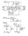
- Fig. 2 is a logic circuit to be checked for the presence of a local delay error, which is connected via its inputs to outputs 9 and 10 of part 1 and via its output to the input 11 of part 2 of a digital circuit by one after Simulation model 12 formed according to the invention.
- the latter contains a simulation stage 13 which, in conjunction with a downstream output stage 14, simulates the logic circuit as if it did not contain a circuit branch with an impermissibly low conductance, but rather a circuit branch with an interruption error.
- Such an interruption error causes signal storage at a circuit point of the logic circuit.
- this circuit point has a capacitance of sufficient size, for example if it simultaneously represents the input of a subsequent field effect transistor stage which is subject to a gate capacitance, and isolation of the circuit point from the upstream, driving part of the logic circuit due to the interruption error occurs, the charge state of the capacity that is present when the interruption fault takes effect remains.
- This effect of charge storage is taken into account by an output stage 14, which is connected with its two inputs to two outputs 15, 16 of the simulation stage 13.
- the output of 14 is designated 17.
- the output stage 14 has the function that it switches through any signal which is not influenced by the interruption error simulated in FIG. 13 and occurs at the output 15 of FIG. 13 to its output 17, but does not switch on this signal when a signal influenced by the simulated error occurs, but instead the continuation of the last signal which occurred before the error-affected signal occurred at 15 continues to be maintained.
- the output stage 14 is controlled as a function of the signals occurring at the outputs 15 and 16 of the simulation stage 13.
- the simulation stage 13 is designed so that whenever a logical "0" appears at both outputs 15 and 16, a through the signal affected by the interruption error is present.
- Figure 1 of this publication shows a CMOS gate and Figure 3 shows the corresponding replica and output stage.
- the output stage 14 is designated as a logical block B, the function table of which, which can be found in table I on page 65, corresponds to that of an RS flip-flop.
- a detector 18 which is connected to the outputs 15 and 16 with its two inputs, it is checked whether the simulation stage 13 is in a switching state in which a logical "0" occurs on both 15 and 16. If this is the case, a logical "1" is output at the output 18a of 18.
- the detector 18 may consist of a NOR gate, for example.
- the output signal from 18 is fed to an evaluator 19, the clock input 19a of which is occupied by clock pulses, which occur at the beginning of the individual clock periods.
- the evaluator 19 checks whether the signal combination 0, 0 is emitted via the outputs 15 and 16 of the simulation stage 13 during two successive clock periods.
- a logic "1" is output via the output 20 of 19, which is fed to the control input of a multiplexer 21. If the signal combination 0, 0 occurs at the outputs 15 and 16 but during two successive clock periods, the evaluator 19 outputs a logical "0" at the output 20.
- the multiplexer 21 now switches when receiving a control signal "1" Signals at its first input, which is connected to the output 17, through to its output 11. On the other hand, when a control signal "0" occurs, the signals present at 17 are switched off by output 11 and instead the signals present at its input 22 are switched through to 11.
- the input 22 is connected to the output of an error-free replica 23, which is driven parallel to the replica stage 13 and is designed such that it simulates the function of the logic circuit to be checked without errors.
- the signal combination 0, 0 remains at the outputs 15 and 16 during two successive clock periods, then the signal stored at 17 is switched off by the output 11 and replaced by the output signal of the error-free replica 23.
- This limits error detection to a single clock period, at the start of which the signal change necessary for error detection occurred at inputs E1 ... En.
- the resultant reduction in the error detectability of an interruption error to a single clock period corresponds entirely to the desired simulation of a local delay error in the logic circuit to be examined.
- FIG. 3 shows an embodiment of the simulation model which differs from FIG. 2 and is denoted here by 12 ⁇ .
- An error-free replica 23 ⁇ of the logic circuit to be checked is provided here, the two inputs of which are connected to the outputs 9 and 10 of part 1 of the digital circuit.
- the output 24 of 23 ⁇ is guided via an output stage 25, the output of which is designated 26, to the first input of the multiplexer 21, while the second input of 21 is connected to the output 24.
- the signal occurring at the switching point 28 and controlling the output stage 25 is also fed to an inverter 29, the output signal of which reaches the evaluator 19.
- the other circuit parts of FIG. 3 correspond to the same-named circuit parts of FIG. 2 in terms of structure and mode of operation.
- the multiplexer 21 is controlled such that instead of the signal present at 26, the signal present at 24, which is not influenced by the interruption error, is switched through to the output 11 of the simulation model 12 ⁇ .
- This control of the multiplexer 21 achieves the simulation of an interruption error which only occurs for the duration of one clock period, but which corresponds to the simulation of a local delay error.
- the evaluator 19 located between the circuit points 18a and 20 of FIG. 2 can expediently be designed according to FIG. 4.
- 18a is connected to the input of a D flip-flop 29.
- the output Q of the same is connected to the first input of a NAND gate 30, the second input of which is connected to 18a.
- the output of 30 corresponds to the circuit point 20 of FIG. 1.
- the circuit point 19a here represents the clock input of the D flip-flop 29. If a logic "1" is present at 18a within a period of time which is longer than a clock period, there is one logic "1" both at input D and at output Q of 29. However, this means that the output of NAND gate 30 is set to "0".
- the multiplexer 21 is thus switched from the output 17 to the output of the error-free simulation 23, as described, so that a simulation of a local delay error is ensured.
- An output 19 designed according to FIG. 4 can also be used in FIG. 3.
- FIG. 5 An advantageous embodiment of the multiplexer 21 is shown in FIG. 5.
- two NAND gates 31 and 32 are provided, the first inputs of which are connected to one another via an inverter 33. Furthermore, the first input of 31 is connected to the output 20 of the evaluator 19.
- the second input of 31 is at the output 17 of the output stage 14, the second input of 32 corresponding to the input 22 of the multiplexer 21.
- the outputs of the AND gates 31 and 32 are connected to the inputs of an OR gate 34, the output of which represents the output 11 of the multiplexer.
- the second input of 31 is at the node 26.
- FIG. 6 shows the circuit design of a simulation stage 13 used in FIG. 2 in the simulation model 12 and an associated output stage 14, which are used to model a NAND gate with two inputs in complementary circuit technology.
- a NAND gate 35 and an AND gate 36 are connected to node 9 with their first inputs, while their second inputs are connected to node 10.
- the output of 35 is connected to the S input of an RS flip-flop 37, the output of 36 to its R input.
- the output Q of the RS flip-flop 37 corresponds to the node 17 of FIG. 2.
- An interruption error in one of the two parallel branches of the simulated NAND gate is simulated by an adhesion error at the first input of 35, an interruption error in the other of the two parallel branches by an adhesion error at the second input of 35.
- These two adhesion errors which are called “stuck-at -1 "errors are in turn simulated by separating the respective input from circuit points 9 and 10 and by applying a level corresponding to a logical" 1 "at the respectively separated input of 35.
- An interruption error in the series branch of the simulated NAND gate is caused by a detention error at the output of 36 simulated.
- This sticking error is designed as a "stuck-at-0" error and is simulated in such a way that the R input of 37 is separated from the output of the AND gate 36 and is assigned a level which corresponds to a logic "0" .
Landscapes
- Engineering & Computer Science (AREA)
- Computer Hardware Design (AREA)
- General Engineering & Computer Science (AREA)
- Theoretical Computer Science (AREA)
- Quality & Reliability (AREA)
- Physics & Mathematics (AREA)
- General Physics & Mathematics (AREA)
- Test And Diagnosis Of Digital Computers (AREA)
- Tests Of Electronic Circuits (AREA)
- Management, Administration, Business Operations System, And Electronic Commerce (AREA)
- Metal-Oxide And Bipolar Metal-Oxide Semiconductor Integrated Circuits (AREA)
- Logic Circuits (AREA)
Priority Applications (1)
| Application Number | Priority Date | Filing Date | Title |
|---|---|---|---|
| AT87107288T ATE87754T1 (de) | 1986-06-06 | 1987-05-19 | Verfahren zur simulation eines verzoegerungsfehlers in einer logikschaltung und anordnungen zur durchfuehrung des verfahrens. |
Applications Claiming Priority (2)
| Application Number | Priority Date | Filing Date | Title |
|---|---|---|---|
| DE3619023 | 1986-06-06 | ||
| DE3619023 | 1986-06-06 |
Publications (3)
| Publication Number | Publication Date |
|---|---|
| EP0248268A2 true EP0248268A2 (fr) | 1987-12-09 |
| EP0248268A3 EP0248268A3 (en) | 1989-05-10 |
| EP0248268B1 EP0248268B1 (fr) | 1993-03-31 |
Family
ID=6302401
Family Applications (1)
| Application Number | Title | Priority Date | Filing Date |
|---|---|---|---|
| EP87107288A Expired - Lifetime EP0248268B1 (fr) | 1986-06-06 | 1987-05-19 | Procédé de simulation d'une erreur de retard dans un circuit logique et dispositifs pour la réalisation dudit procédé |
Country Status (5)
| Country | Link |
|---|---|
| US (1) | US4852093A (fr) |
| EP (1) | EP0248268B1 (fr) |
| JP (1) | JPS62290941A (fr) |
| AT (1) | ATE87754T1 (fr) |
| DE (1) | DE3785083D1 (fr) |
Families Citing this family (17)
| Publication number | Priority date | Publication date | Assignee | Title |
|---|---|---|---|---|
| US5023875A (en) * | 1989-05-26 | 1991-06-11 | Hughes Aircraft Company | Interlaced scan fault detection system |
| US5173896A (en) * | 1990-11-30 | 1992-12-22 | Bell Atlantic Network Services, Inc. | T-carrier network simulator |
| US5206583A (en) * | 1991-08-20 | 1993-04-27 | International Business Machines Corporation | Latch assisted fuse testing for customized integrated circuits |
| US5884065A (en) * | 1992-01-10 | 1999-03-16 | Nec Corporation | Logic circuit apparatus and method for sequentially performing one of a fault-free simulation and a fault simulation through various levels of a logic circuit |
| JPH05203708A (ja) * | 1992-01-28 | 1993-08-10 | Fujitsu Ltd | 順序回路の縮退故障テスト方法 |
| JP2708314B2 (ja) * | 1992-04-09 | 1998-02-04 | 三菱電機株式会社 | 論理シミュレーション装置 |
| JP3124417B2 (ja) * | 1993-07-13 | 2001-01-15 | 三菱電機株式会社 | 論理シミュレーションシステム及び論理シミュレーション方法 |
| US5495598A (en) * | 1993-12-23 | 1996-02-27 | Unisys Corporation | Stuck fault detection for branch instruction condition signals |
| DE69533567T2 (de) * | 1994-08-09 | 2005-11-24 | Sun Microsystems, Inc., Mountain View | Vorrichtung und Verfahren zum Auffinden von False-Timing-Paths in digitalen Schaltkreisen |
| US5761488A (en) * | 1996-06-13 | 1998-06-02 | International Business Machines Corporation | Logic translation method for increasing simulation emulation efficiency |
| DE10296364T5 (de) * | 2001-02-23 | 2004-04-22 | Telefonaktiebolaget Lm Ericsson (Publ) | Eine Testschaltung zum Verifizieren eines Herstellungsprozesses |
| JP2003233639A (ja) * | 2002-02-06 | 2003-08-22 | Mitsubishi Electric Corp | 故障検証装置、故障検証方法および故障解析手法 |
| US7216281B2 (en) * | 2004-09-29 | 2007-05-08 | Advantest Corp. | Format control circuit and semiconductor test device |
| JP5262985B2 (ja) * | 2009-05-19 | 2013-08-14 | 富士通株式会社 | 遅延故障検査プログラム、遅延故障検査装置、および遅延故障検査方法 |
| JP5262996B2 (ja) * | 2009-05-26 | 2013-08-14 | 富士通セミコンダクター株式会社 | 論理シミュレーション装置、方法、及びプログラム |
| US10950421B2 (en) * | 2014-04-21 | 2021-03-16 | Lam Research Corporation | Using modeling for identifying a location of a fault in an RF transmission system for a plasma system |
| US10936474B2 (en) * | 2017-12-13 | 2021-03-02 | Arm Limited | Software test program generation |
Family Cites Families (9)
| Publication number | Priority date | Publication date | Assignee | Title |
|---|---|---|---|---|
| US3633100A (en) * | 1970-05-12 | 1972-01-04 | Ibm | Testing of nonlinear circuits by comparison with a reference simulation with means to eliminate errors caused by critical race conditions |
| US3715573A (en) * | 1971-04-14 | 1973-02-06 | Ibm | Failure activity determination technique in fault simulation |
| US3780277A (en) * | 1972-07-13 | 1973-12-18 | Bell Telephone Labor Inc | Apparatus for propagating internal logic gate faults in a digital logic simulator |
| US4156132A (en) * | 1977-11-01 | 1979-05-22 | Burroughs Corporation | Automatic fault injection apparatus and method |
| US4242751A (en) * | 1978-08-28 | 1980-12-30 | Genrad, Inc. | Automatic fault-probing method and apparatus for checking electrical circuits and the like |
| US4228537A (en) * | 1978-08-29 | 1980-10-14 | Genrad, Inc. | Method of and apparatus for automatic fault diagnosis of electrical circuits employing on-line simulation of faults in such circuits during diagnosis |
| JPS55153054A (en) * | 1979-05-15 | 1980-11-28 | Hitachi Ltd | Logic circuit simulation system |
| US4308616A (en) * | 1979-05-29 | 1981-12-29 | Timoc Constantin C | Structure for physical fault simulation of digital logic |
| FR2567273B1 (fr) * | 1984-07-03 | 1986-11-14 | Commissariat Energie Atomique | Dispositif de simulation de la defaillance ou du bon fonctionnement d'un systeme logique |
-
1987
- 1987-05-19 AT AT87107288T patent/ATE87754T1/de not_active IP Right Cessation
- 1987-05-19 DE DE8787107288T patent/DE3785083D1/de not_active Expired - Fee Related
- 1987-05-19 EP EP87107288A patent/EP0248268B1/fr not_active Expired - Lifetime
- 1987-06-03 US US07/056,896 patent/US4852093A/en not_active Expired - Fee Related
- 1987-06-03 JP JP62140726A patent/JPS62290941A/ja active Pending
Also Published As
| Publication number | Publication date |
|---|---|
| JPS62290941A (ja) | 1987-12-17 |
| US4852093A (en) | 1989-07-25 |
| ATE87754T1 (de) | 1993-04-15 |
| EP0248268B1 (fr) | 1993-03-31 |
| DE3785083D1 (de) | 1993-05-06 |
| EP0248268A3 (en) | 1989-05-10 |
Similar Documents
| Publication | Publication Date | Title |
|---|---|---|
| EP0248268B1 (fr) | Procédé de simulation d'une erreur de retard dans un circuit logique et dispositifs pour la réalisation dudit procédé | |
| DE3689228T2 (de) | Verfahren zur Modellierung und zur Fehlersimulation von komplementären Metalloxidhalbleiterschaltungen. | |
| DE2311034C2 (de) | Verfahren zum Prüfen eines integrierte logische Verknüpfungs- und Speicherglieder enthaltenden Halbleiterchips | |
| DE2121115C2 (de) | Prüfeinrichtung für nichtlineare Schaltkreise | |
| DE2023741A1 (de) | Testeinrichtung für komplexe, eine Vielzahl von Anschlußstiften aufweisende Funktionslogikschaltungen | |
| DE68921086T2 (de) | Integrierte Halbleiterschaltkreisanordnung mit verbesserter Eingangs-/ Ausgangsschnittstellenschaltung. | |
| DE2723707C2 (de) | Schaltung zur Erzeugung nicht-überlappender Taktimpuls-Züge | |
| DE3702408C2 (fr) | ||
| EP0010173A1 (fr) | Plaquette à semiconducteur avec une possibilité de test améliorée des circuits intégrés monolithiques à grande échelle | |
| DE69017169T2 (de) | Testen integrierter Schaltungen unter Verwendung von Taktgeberstössen. | |
| DE2329610A1 (de) | Fehlersimulation zur bestimmung der pruefbarkeit von nichtlinearen integrierten schaltungen | |
| DE10129329A1 (de) | Fehlersimulationsverfahren und Fehlersimulator für einen Halbleiter-IC | |
| DE69724742T2 (de) | Speicherfeldprüfschaltung mit Fehlermeldung | |
| EP0203535B1 (fr) | Méthode pour la simulation d'une erreur dans un circuit logique et dispositif pour la réalisation d'une telle méthode | |
| DE3889140T2 (de) | On-chip, On-line-Wechselstrom und Gleichstromfehlererkennungssystem für Taktbaum. | |
| EP0628832A2 (fr) | Circuit intégré comportant des étages de registres | |
| EP0248269B1 (fr) | Procédé de simulation d'une erreur de "circuit ouvert" d'un circuit logique à transistor à effet de champ et dispositifs pour la réalisation dudit procédé | |
| EP0186040A1 (fr) | Mémoire intégrée à semi-conducteur | |
| DE3486064T2 (de) | Logische schaltung mit eingebauter selbsttestfunktion. | |
| DE3688437T2 (de) | Verfahren zur Umwandlung einer MOS-Schaltung von Schaltebenedarstellung in eine boolesche Darstellung und Verfahren zur Fehlersimulation in einer auf der Schaltebene dargestellten MOS-Schaltung durch das Verwenden seiner booleschen Darstellung. | |
| DE10328719B4 (de) | Verfahren zum Testen von elektronischen Bauteilen | |
| DE19624858A1 (de) | Integrierte Schaltung mit Testfunktion | |
| DE1945138C3 (de) | Verfahren und Einrichtung zur Prüfung einer elektrischen Verdrahtung auf fehlende und überzählige Verbindungen | |
| DE2824862A1 (de) | Monolithisch integrierte digitale halbleiterschaltung | |
| DE3401292C2 (fr) |
Legal Events
| Date | Code | Title | Description |
|---|---|---|---|
| PUAI | Public reference made under article 153(3) epc to a published international application that has entered the european phase |
Free format text: ORIGINAL CODE: 0009012 |
|
| AK | Designated contracting states |
Kind code of ref document: A2 Designated state(s): AT DE FR GB IT NL |
|
| PUAL | Search report despatched |
Free format text: ORIGINAL CODE: 0009013 |
|
| AK | Designated contracting states |
Kind code of ref document: A3 Designated state(s): AT DE FR GB IT NL |
|
| 17P | Request for examination filed |
Effective date: 19891026 |
|
| 17Q | First examination report despatched |
Effective date: 19910808 |
|
| GRAA | (expected) grant |
Free format text: ORIGINAL CODE: 0009210 |
|
| AK | Designated contracting states |
Kind code of ref document: B1 Designated state(s): AT DE FR GB IT NL |
|
| REF | Corresponds to: |
Ref document number: 87754 Country of ref document: AT Date of ref document: 19930415 Kind code of ref document: T |
|
| REF | Corresponds to: |
Ref document number: 3785083 Country of ref document: DE Date of ref document: 19930506 |
|
| ITF | It: translation for a ep patent filed | ||
| ET | Fr: translation filed | ||
| GBT | Gb: translation of ep patent filed (gb section 77(6)(a)/1977) |
Effective date: 19930615 |
|
| PGFP | Annual fee paid to national office [announced via postgrant information from national office to epo] |
Ref country code: DE Payment date: 19930720 Year of fee payment: 7 |
|
| PLBE | No opposition filed within time limit |
Free format text: ORIGINAL CODE: 0009261 |
|
| STAA | Information on the status of an ep patent application or granted ep patent |
Free format text: STATUS: NO OPPOSITION FILED WITHIN TIME LIMIT |
|
| 26N | No opposition filed | ||
| PGFP | Annual fee paid to national office [announced via postgrant information from national office to epo] |
Ref country code: GB Payment date: 19940418 Year of fee payment: 8 |
|
| PGFP | Annual fee paid to national office [announced via postgrant information from national office to epo] |
Ref country code: AT Payment date: 19940422 Year of fee payment: 8 |
|
| PGFP | Annual fee paid to national office [announced via postgrant information from national office to epo] |
Ref country code: FR Payment date: 19940519 Year of fee payment: 8 |
|
| PGFP | Annual fee paid to national office [announced via postgrant information from national office to epo] |
Ref country code: NL Payment date: 19940531 Year of fee payment: 8 |
|
| PG25 | Lapsed in a contracting state [announced via postgrant information from national office to epo] |
Ref country code: DE Effective date: 19950201 |
|
| PG25 | Lapsed in a contracting state [announced via postgrant information from national office to epo] |
Ref country code: GB Effective date: 19950519 Ref country code: AT Effective date: 19950519 |
|
| PG25 | Lapsed in a contracting state [announced via postgrant information from national office to epo] |
Ref country code: NL Effective date: 19951201 |
|
| GBPC | Gb: european patent ceased through non-payment of renewal fee |
Effective date: 19950519 |
|
| NLV4 | Nl: lapsed or anulled due to non-payment of the annual fee |
Effective date: 19951201 |
|
| PG25 | Lapsed in a contracting state [announced via postgrant information from national office to epo] |
Ref country code: FR Effective date: 19960229 |
|
| REG | Reference to a national code |
Ref country code: FR Ref legal event code: ST |
|
| REG | Reference to a national code |
Ref country code: FR Ref legal event code: ST |
|
| PG25 | Lapsed in a contracting state [announced via postgrant information from national office to epo] |
Ref country code: IT Free format text: LAPSE BECAUSE OF NON-PAYMENT OF DUE FEES;WARNING: LAPSES OF ITALIAN PATENTS WITH EFFECTIVE DATE BEFORE 2007 MAY HAVE OCCURRED AT ANY TIME BEFORE 2007. THE CORRECT EFFECTIVE DATE MAY BE DIFFERENT FROM THE ONE RECORDED. Effective date: 20050519 |