EP0248325A2 - Procédé pour tester les connexions établies d'un réseau de commutation à large bande - Google Patents
Procédé pour tester les connexions établies d'un réseau de commutation à large bande Download PDFInfo
- Publication number
- EP0248325A2 EP0248325A2 EP87107617A EP87107617A EP0248325A2 EP 0248325 A2 EP0248325 A2 EP 0248325A2 EP 87107617 A EP87107617 A EP 87107617A EP 87107617 A EP87107617 A EP 87107617A EP 0248325 A2 EP0248325 A2 EP 0248325A2
- Authority
- EP
- European Patent Office
- Prior art keywords
- connection
- signal
- test
- blt
- broadband
- Prior art date
- Legal status (The legal status is an assumption and is not a legal conclusion. Google has not performed a legal analysis and makes no representation as to the accuracy of the status listed.)
- Granted
Links
Images
Classifications
-
- H—ELECTRICITY
- H04—ELECTRIC COMMUNICATION TECHNIQUE
- H04Q—SELECTING
- H04Q11/00—Selecting arrangements for multiplex systems
- H04Q11/04—Selecting arrangements for multiplex systems for time-division multiplexing
- H04Q11/0428—Integrated services digital network, i.e. systems for transmission of different types of digitised signals, e.g. speech, data, telecentral, television signals
- H04Q11/0478—Provisions for broadband connections
-
- H—ELECTRICITY
- H04—ELECTRIC COMMUNICATION TECHNIQUE
- H04Q—SELECTING
- H04Q1/00—Details of selecting apparatus or arrangements
- H04Q1/18—Electrical details
- H04Q1/20—Testing circuits or apparatus; Circuits or apparatus for detecting, indicating, or signalling faults or troubles
- H04Q1/22—Automatic arrangements
- H04Q1/24—Automatic arrangements for connection devices
- H04Q1/245—Automatic arrangements for connection devices in time-division multiplex systems
-
- H—ELECTRICITY
- H04—ELECTRIC COMMUNICATION TECHNIQUE
- H04J—MULTIPLEX COMMUNICATION
- H04J2203/00—Aspects of optical multiplex systems other than those covered by H04J14/05 and H04J14/07
- H04J2203/0001—Provisions for broadband connections in integrated services digital network using frames of the Optical Transport Network [OTN] or using synchronous transfer mode [STM], e.g. SONET, SDH
- H04J2203/0003—Switching fabrics, e.g. transport network, control network
Definitions
- interconnection tests In order to determine faulty connections in switching systems, their coupling devices are subjected to so-called interconnection tests.
- the concept of such an interconnection test must take into account the size of the switching system, switching processes and, if necessary, a division of tasks between different switching processors.
- test information in each case comprises a sender address which identifies the input of the switching device used for the connection in question and a destination address which identifies the output of the switching device to be used is compared on the receiving side with the connection data formed by these addresses, in a telecommunications system in which operating information serving for signaling, control and synchronization is also transmitted on the lines to be connected by the space multiplex coupling device in periodically repeating periods in addition to the user information to be switched through, either the test information is only transmitted during the establishment of the connection in the time periods provided for the useful information and a comparison is made once on the test information in each case comprises a sender address which identifies the input of the switching device used for the connection in question and a destination address which identifies the output of the switching device to be used is compared on the receiving side with the connection data formed by these addresses, in a telecommunications system in which operating information serving for signaling, control and synchronization is also transmitted on the lines to be connected by the space multiplex coupling device in periodically repeating periods in addition
- This interconnection test makes it possible to identify connections in one direction and (in particular. Crosstalk-related) double connections that have already been made in a faulty manner from an affected line connection without the involvement of higher-level facilities, so that they do not become effective at all.
- the digital signals transmitted through the broadband coupling device can also be sent individually to a test that is also connected to the broadband coupling device connection can be switched on.
- Such a test connection which can be connected cyclically or on a case-by-case basis to the individual line connections, can take the circuit test signals contained therein from the digital signal and pass them on to the associated switching processor, which can thus check the accuracy of the existing connection.
- additional signaling bits can also be transmitted to the test connection, which the test connection can then evaluate and forward to the switching processor.
- the connection circuits themselves to transmit message bits to the superordinate switching processor via separate message signal connections, which in turn can receive corresponding additional information.
- this known procedure enables a decentralized, purely connection-related through-connection test of a broadband coupling device, even without special test connections and thus avoiding the circumstances associated with the use of test connections, such as the requirement in a control process for the assignment of one of the having to wait in a limited number of available test connections or the need for additional processes for routine tests of semi-permanent connections, - so that the respective switching processor is spared corresponding coordination services.
- the object of the invention is now to further decentralize the interconnection test of a broadband switching device.
- the invention relates to a method for the through-connection test of a broadband switching device with connection-specific input-side feeding and output-side evaluation of a test signal containing an address identifying the switching device input.
- this method is characterized in that in one of the two connection circuits involved in a connection, the interconnection test signals received from the counter-connection circuit are checked for the occurrence of both the own address and the address of the counter-connection circuit, and at least one of the at least if no one occurs Both addresses a signal reporting the test result is transmitted from the connection circuit to the associated switching processor.
- Such an interconnection test with a somewhat asymmetrical evaluation of the interconnection test signals enables the addresses of the two connection circuits involved in a connection to be combined in such a connection circuit itself and thus avoids a corresponding load on the associated switching processor; rather, the switching processor can already have the addresses of both ports involved in use circuits together from the relevant take over a connection circuit.
- the circuit test signals can be continuously checked for (sustainable) changes in the connection circuit in question, and in a further embodiment of the invention a signal is then only transmitted after a change in the circuit test signal, which leads to a correspondingly low load on the switching processor by such signal signals.
- circuit test signals in the connection circuit in question are constantly compared with a target signal specified by the associated switching processor in accordance with the respective connection state, and in a further embodiment of the invention a message signal is then only transmitted if the circuit test signal differs from the respective target signal, which also leads to a correspondingly low load on the switching processor.
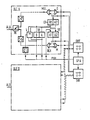
- an embodiment of an integrated service telecommunication system with a narrowband switching device SKF controlled by a switching processor GP A and a separate broadband switching device BKF, preferably controlled by the same switching processor GP A, to the to subscriber stations or to is shown schematically to an extent necessary for understanding the invention other switching devices leading fiber optic connection lines AL A, .. .., AL B are each connected via a connection circuit BLT A, ..., BLT B.
- connection circuits can each be grouped into a plurality of (subscriber) connections, each with a group coupler and a group processor (decentralized) connection groups and that the telecommunication system can also have a central switching network and a central coordination processor.
- the coupling device shown in the drawing then stands for the respective group coupler and / or the central switching network and the switching processor GP A shown in the drawing for the group processor and / or the central coordination processor.
- connection circuit BLT A in more detail in terms of circuitry, it can be seen that the - then single-fiber - optical fiber connecting line AL in the connection circuit BLT via an optical fiber directional coupler RK with the output of an electro / optical converter e / o and with the Input of an opto / electrical converter o / e can be connected.
- the output of a multiplexer MUL is connected to the input of the electro / optical converter e / o, which transmits narrowband digital signals (e.g. 64 kbit / telephone signals) via the narrowband coupling device SKF and broadband signals (image signals) transmitted via the broadband coupling device BKF and (e.g.
- the opto / electrical converter eg 8 kbit / s
- each the address of this connection circuit BLT and possibly the corresponding received from the opposite side via the broadband switching device BKF Switch-through test signals contain the address of a counter-connection circuit.
- a transmit register SR can be provided for this in each connection circuit BLT, in the first register part A1 of which the switching processor GP A entered (or also constantly) the address of this connection circuit may be located and in the second register part thereof B2 if necessary, the received address of a counter-connection circuit is entered; on the output side, the transmission register SR leads to a corresponding input of a multiplexer M, which is inserted between the demultiplexer DEX and the broadband coupling device BKF, so that it inserts the interconnection test signal emitted by the transmission register SR into a signal gap of the broadband signal.
- the invention can also be used when no narrowband signal is actually transmitted on the connecting line AL; it is rather sufficient to assume that a narrow-band (for example 4 kbit / s) signal gap (for example in the form of a bit position in every other frame) is available in the broadband signal for receiving the circuit test signal.
- a narrow-band (for example 4 kbit / s) signal gap for example in the form of a bit position in every other frame
- a demultiplexer D is inserted in the reverse signal path between the broadband switching device BKF and the multiplexer MUL.
- Its first register part B1 which possibly contains the address contained in such a circuit test signal of a counter-connection circuit currently connected to the connection circuit BLT A under consideration via the broadband switching device BKF, for example the connection circuit BLT B constructed in the same way, is with the transmission register part B2 connected so that the address of the counter-connection circuit (BLT B) contained in the connection circuit BLT A received in this transmission register part B2 and then, as already mentioned, in the connection test signals to be subsequently emitted by the connection circuit BLT A under consideration to the address just added this connection circuit BLT A and is thus transmitted back to the counter-connection circuit (BLT B).
- connection circuit BLT B connected to the connection circuit BLT A via the broadband coupling device BKF in the example, the address of the connection circuit contained in the circuit test signals received there by the connection circuit BLT A BLT A is reflected to a certain extent in the interconnection test signals emitted by the connection circuit BLT B.
- the reflected address then arrives in the connection circuit BLT A in its reception register part A2.
- connection circuit BLT In one of the two connection circuits BLT involved in a connection, for example in the connection circuit of the calling subscriber, the interconnection test signals received from the counter-connection circuit are now checked for the occurrence of both the own address and the address of the counter-connection circuit.
- connection circuit BLT A it is indicated for the connection circuit BLT A that a comparator V compares the two addresses which have just entered the reception register ER with the circuit test signal just received with two corresponding addresses in a comparison register VR in corresponding register parts A and B.
- the two addresses contained in the most recently received circuit test signal can be found in the comparison register VR, so that the comparator V can then determine changes in the circuit test signal;
- a signal reporting the test result is then transmitted from the connection circuit BLT A via a corresponding message signal connection msv to the associated switching processor GP A, which then transmits the two connection circuit addresses from the connection circuit BLT A via the message signal connection msv can take to draw appropriate conclusions.
- the comparator V is expediently provided with a drop-out delay, so that the signal transmission when there is a change in the switching test signal for a delay period t2 is omitted and thus individual errors in the transmission of the switching test signals do not lead to a signaling signal.
- the switching processor is largely exempt from control services for testing and monitoring the switching network:
- the connection circuit BLT on the calling connection side reports itself with the addresses of the connection circuits involved in the connection as soon as the connection is set in the switching network; faulty connections are expressed in wrong addresses.
- the connection circuit BLT on the calling connection side reacting spontaneously when a connection error occurs.
- the circuits performing the interconnection test or connection monitoring are also tested in operation, but a targeted test by switching pseudo connections in the switching network is not excluded.
Landscapes
- Engineering & Computer Science (AREA)
- Computer Networks & Wireless Communication (AREA)
- Data Exchanges In Wide-Area Networks (AREA)
- Channel Selection Circuits, Automatic Tuning Circuits (AREA)
- Circuits Of Receivers In General (AREA)
- Detection And Prevention Of Errors In Transmission (AREA)
- Two-Way Televisions, Distribution Of Moving Picture Or The Like (AREA)
Priority Applications (1)
| Application Number | Priority Date | Filing Date | Title |
|---|---|---|---|
| AT87107617T ATE101952T1 (de) | 1986-06-02 | 1987-05-25 | Verfahren zur durchschaltepruefung einer breitband-koppeleinrichtung. |
Applications Claiming Priority (2)
| Application Number | Priority Date | Filing Date | Title |
|---|---|---|---|
| DE3618522 | 1986-06-02 | ||
| DE3618522 | 1986-06-02 |
Publications (3)
| Publication Number | Publication Date |
|---|---|
| EP0248325A2 true EP0248325A2 (fr) | 1987-12-09 |
| EP0248325A3 EP0248325A3 (en) | 1989-12-20 |
| EP0248325B1 EP0248325B1 (fr) | 1994-02-23 |
Family
ID=6302125
Family Applications (1)
| Application Number | Title | Priority Date | Filing Date |
|---|---|---|---|
| EP87107617A Expired - Lifetime EP0248325B1 (fr) | 1986-06-02 | 1987-05-25 | Procédé pour tester les connexions établies d'un réseau de commutation à large bande |
Country Status (3)
| Country | Link |
|---|---|
| EP (1) | EP0248325B1 (fr) |
| AT (1) | ATE101952T1 (fr) |
| DE (1) | DE3789123D1 (fr) |
Cited By (1)
| Publication number | Priority date | Publication date | Assignee | Title |
|---|---|---|---|---|
| DE3821871A1 (de) * | 1988-06-29 | 1990-01-18 | Philips Patentverwaltung | Breitbandkoppeleinrichtung |
Family Cites Families (3)
| Publication number | Priority date | Publication date | Assignee | Title |
|---|---|---|---|---|
| US4439826A (en) * | 1981-07-20 | 1984-03-27 | International Telephone & Telegraph Corporation | Diagnostic system for a distributed control switching network |
| EP0163288B1 (fr) * | 1984-05-29 | 1988-11-23 | Siemens Aktiengesellschaft | Méthode pour tester des chemins commutés d'un réseau de connexion multiplex à division dans l'espace |
| JPS6148266A (ja) * | 1984-08-15 | 1986-03-08 | Fujitsu Ltd | 時分割多重回線折返試験方法 |
-
1987
- 1987-05-25 DE DE87107617T patent/DE3789123D1/de not_active Expired - Fee Related
- 1987-05-25 AT AT87107617T patent/ATE101952T1/de not_active IP Right Cessation
- 1987-05-25 EP EP87107617A patent/EP0248325B1/fr not_active Expired - Lifetime
Cited By (1)
| Publication number | Priority date | Publication date | Assignee | Title |
|---|---|---|---|---|
| DE3821871A1 (de) * | 1988-06-29 | 1990-01-18 | Philips Patentverwaltung | Breitbandkoppeleinrichtung |
Also Published As
| Publication number | Publication date |
|---|---|
| EP0248325B1 (fr) | 1994-02-23 |
| DE3789123D1 (de) | 1994-03-31 |
| EP0248325A3 (en) | 1989-12-20 |
| ATE101952T1 (de) | 1994-03-15 |
Similar Documents
| Publication | Publication Date | Title |
|---|---|---|
| EP0631412A2 (fr) | Procédé et dispositif pour la transmission de paquets ATM | |
| DE3902243A1 (de) | Verfahren zum schalten von digitalsignal-verbindungen in uebertragungsnetzen | |
| DE2714368C3 (de) | Schaltungsanordnung zum Durchschalten von Datenwörtern unterschiedlicher Bitfolgefrequenz in Vielfachverbindungen | |
| DE69634149T2 (de) | Optischer knoten in einem optischen busnetz | |
| DE3937738A1 (de) | Teilnehmeranschlussknoten eines digitalen nachrichtenuebertragungssystems | |
| EP0163288B1 (fr) | Méthode pour tester des chemins commutés d'un réseau de connexion multiplex à division dans l'espace | |
| EP0173274B1 (fr) | Méthode et montage pour la réalisation et la maintenance d'une liaison à division temporelle à large bande | |
| EP0248325B1 (fr) | Procédé pour tester les connexions établies d'un réseau de commutation à large bande | |
| EP0284106A2 (fr) | Dispositif pour intercaler une voie de service pour un système de transmission | |
| EP0193967B1 (fr) | Procédé pour tester une connexion d'un réseau de commutation à large bande | |
| EP0198203B1 (fr) | Procédé pour tester une connexion d'un réseau de commutation à large bande | |
| EP0126413B1 (fr) | Système de télécommunication à la fois pour trafic en mode-circuit et pour trafic en mode-paquet | |
| DE2316478C3 (de) | Verfahren zur Prüfung und Aufrechterhaltung der Funktionsfähigkeit eines Zeitmultiplex-Vermittlungsnetzes | |
| DE3789137T2 (de) | Verfahren zur Erweiterung der Uebertragungskapazität in einem Netzwerkübertragungssystem für optische Teilnehmer. | |
| DE3821871C2 (fr) | ||
| DE3513165A1 (de) | Schaltungsanordnung fuer fernmeldevermittlungsanlagen, insbesondere fernsprechvermittlungsanlagen, mit einrichtungen zur funktionsfaehigkeitspruefung durchgeschalteter verbindungen | |
| AT390857B (de) | Schaltungsanordnung zum vermitteln von datensignalen unterschiedlicher datensignalraten in einer datenvermittlungsanlage | |
| EP0023297B1 (fr) | Système de télécommunication numérique | |
| DE69434309T2 (de) | Faseroptisches digitales Kommunikationssystem mit Zeitmultiplexmehrfachzugriff | |
| DE3932700C2 (de) | Verfahren zur Durchschalteprüfung eines Koppelnetzes | |
| DE2849348C2 (fr) | ||
| DE3513181A1 (de) | Schaltungsanordnung fuer fernmeldevermittlungsanlagen, insbesondere fernsprechvermittlungsanlagen, mit einrichtungen zur funktionsfaehigkeitspruefung durchgeschalteter verbindungen | |
| DE19549149A1 (de) | Verfahren zur Steuerung der Übertragung von digitalen Nachrichtensignalen über ein Zeitmultiplex-Übertragungsmedium | |
| DE19530783C2 (de) | Verfahren zur digitalen Übertragung von nachrichtentechnischen Diensten | |
| DE3307347C2 (fr) |
Legal Events
| Date | Code | Title | Description |
|---|---|---|---|
| PUAI | Public reference made under article 153(3) epc to a published international application that has entered the european phase |
Free format text: ORIGINAL CODE: 0009012 |
|
| AK | Designated contracting states |
Kind code of ref document: A2 Designated state(s): AT BE CH DE FR GB IT LI NL SE |
|
| PUAL | Search report despatched |
Free format text: ORIGINAL CODE: 0009013 |
|
| AK | Designated contracting states |
Kind code of ref document: A3 Designated state(s): AT BE CH DE FR GB IT LI NL SE |
|
| 17P | Request for examination filed |
Effective date: 19900528 |
|
| 17Q | First examination report despatched |
Effective date: 19920310 |
|
| GRAA | (expected) grant |
Free format text: ORIGINAL CODE: 0009210 |
|
| AK | Designated contracting states |
Kind code of ref document: B1 Designated state(s): AT BE CH DE FR GB IT LI NL SE |
|
| PG25 | Lapsed in a contracting state [announced via postgrant information from national office to epo] |
Ref country code: IT Free format text: LAPSE BECAUSE OF FAILURE TO SUBMIT A TRANSLATION OF THE DESCRIPTION OR TO PAY THE FEE WITHIN THE PRE;WARNING: LAPSES OF ITALIAN PATENTS WITH EFFECTIVE DATE BEFORE 2007 MAY HAVE OCCURRED AT ANY TIME BEFORE 2007. THE CORRECT EFFECTIVE DATE MAY BE DIFFERENT FROM THE ONE RECORDED.SCRIBED TIME-LIMIT Effective date: 19940223 Ref country code: BE Effective date: 19940223 |
|
| REF | Corresponds to: |
Ref document number: 101952 Country of ref document: AT Date of ref document: 19940315 Kind code of ref document: T |
|
| REF | Corresponds to: |
Ref document number: 3789123 Country of ref document: DE Date of ref document: 19940331 |
|
| GBT | Gb: translation of ep patent filed (gb section 77(6)(a)/1977) |
Effective date: 19940429 |
|
| ET | Fr: translation filed | ||
| PLBE | No opposition filed within time limit |
Free format text: ORIGINAL CODE: 0009261 |
|
| STAA | Information on the status of an ep patent application or granted ep patent |
Free format text: STATUS: NO OPPOSITION FILED WITHIN TIME LIMIT |
|
| EAL | Se: european patent in force in sweden |
Ref document number: 87107617.0 |
|
| 26N | No opposition filed | ||
| PGFP | Annual fee paid to national office [announced via postgrant information from national office to epo] |
Ref country code: GB Payment date: 19970418 Year of fee payment: 11 |
|
| PGFP | Annual fee paid to national office [announced via postgrant information from national office to epo] |
Ref country code: AT Payment date: 19970512 Year of fee payment: 11 |
|
| PGFP | Annual fee paid to national office [announced via postgrant information from national office to epo] |
Ref country code: SE Payment date: 19970516 Year of fee payment: 11 |
|
| PGFP | Annual fee paid to national office [announced via postgrant information from national office to epo] |
Ref country code: FR Payment date: 19970521 Year of fee payment: 11 |
|
| PGFP | Annual fee paid to national office [announced via postgrant information from national office to epo] |
Ref country code: NL Payment date: 19970523 Year of fee payment: 11 |
|
| PGFP | Annual fee paid to national office [announced via postgrant information from national office to epo] |
Ref country code: DE Payment date: 19970721 Year of fee payment: 11 |
|
| PGFP | Annual fee paid to national office [announced via postgrant information from national office to epo] |
Ref country code: CH Payment date: 19970819 Year of fee payment: 11 |
|
| PG25 | Lapsed in a contracting state [announced via postgrant information from national office to epo] |
Ref country code: AT Free format text: LAPSE BECAUSE OF NON-PAYMENT OF DUE FEES Effective date: 19980525 Ref country code: GB Free format text: LAPSE BECAUSE OF NON-PAYMENT OF DUE FEES Effective date: 19980525 |
|
| PG25 | Lapsed in a contracting state [announced via postgrant information from national office to epo] |
Ref country code: SE Free format text: LAPSE BECAUSE OF NON-PAYMENT OF DUE FEES Effective date: 19980526 |
|
| PG25 | Lapsed in a contracting state [announced via postgrant information from national office to epo] |
Ref country code: FR Free format text: LAPSE BECAUSE OF NON-PAYMENT OF DUE FEES Effective date: 19980531 Ref country code: LI Free format text: LAPSE BECAUSE OF NON-PAYMENT OF DUE FEES Effective date: 19980531 Ref country code: CH Free format text: LAPSE BECAUSE OF NON-PAYMENT OF DUE FEES Effective date: 19980531 |
|
| PG25 | Lapsed in a contracting state [announced via postgrant information from national office to epo] |
Ref country code: NL Free format text: LAPSE BECAUSE OF NON-PAYMENT OF DUE FEES Effective date: 19981201 |
|
| GBPC | Gb: european patent ceased through non-payment of renewal fee |
Effective date: 19980525 |
|
| REG | Reference to a national code |
Ref country code: CH Ref legal event code: PL |
|
| EUG | Se: european patent has lapsed |
Ref document number: 87107617.0 |
|
| NLV4 | Nl: lapsed or anulled due to non-payment of the annual fee |
Effective date: 19981201 |
|
| PG25 | Lapsed in a contracting state [announced via postgrant information from national office to epo] |
Ref country code: DE Free format text: LAPSE BECAUSE OF NON-PAYMENT OF DUE FEES Effective date: 19990302 |
|
| REG | Reference to a national code |
Ref country code: FR Ref legal event code: ST |