EP0248355B1 - Mémoire magnétique - Google Patents
Mémoire magnétique Download PDFInfo
- Publication number
- EP0248355B1 EP0248355B1 EP87107788A EP87107788A EP0248355B1 EP 0248355 B1 EP0248355 B1 EP 0248355B1 EP 87107788 A EP87107788 A EP 87107788A EP 87107788 A EP87107788 A EP 87107788A EP 0248355 B1 EP0248355 B1 EP 0248355B1
- Authority
- EP
- European Patent Office
- Prior art keywords
- bit
- film
- intermediate layer
- memory
- structures
- Prior art date
- Legal status (The legal status is an assumption and is not a legal conclusion. Google has not performed a legal analysis and makes no representation as to the accuracy of the status listed.)
- Expired
Links
Images

Classifications
-
- G—PHYSICS
- G11—INFORMATION STORAGE
- G11C—STATIC STORES
- G11C11/00—Digital stores characterised by the use of particular electric or magnetic storage elements; Storage elements therefor
- G11C11/02—Digital stores characterised by the use of particular electric or magnetic storage elements; Storage elements therefor using magnetic elements
- G11C11/14—Digital stores characterised by the use of particular electric or magnetic storage elements; Storage elements therefor using magnetic elements using thin-film elements
- G11C11/15—Digital stores characterised by the use of particular electric or magnetic storage elements; Storage elements therefor using magnetic elements using thin-film elements using multiple magnetic layers
-
- G—PHYSICS
- G11—INFORMATION STORAGE
- G11C—STATIC STORES
- G11C11/00—Digital stores characterised by the use of particular electric or magnetic storage elements; Storage elements therefor
- G11C11/02—Digital stores characterised by the use of particular electric or magnetic storage elements; Storage elements therefor using magnetic elements
- G11C11/14—Digital stores characterised by the use of particular electric or magnetic storage elements; Storage elements therefor using magnetic elements using thin-film elements
Definitions
- the present invention relates to ferromagnetic thin film memories.
- Digital memories are used very extensively in computers and computer system components, in digital signal processing systems, and in other devices based on digital circuits.
- memories based on storage in electrical circuits in monolithic integrated circuit have become dominant.
- integrated circuit or semiconductor memories still have shortcomings with respect to what is desired in such memories. Primarily they are a) such semiconductor memories lose information upon loss of electrical power, b) they consume electrical power continually during use, and c) they are subject to having the information content thereof scrambled in the presence of impinging radiation.
- Such shortcomings can be overcome by the use of memories where bit storage is based on alternative states of magnetization in magnetic materials used in each memory cell, typically thin film materials.
- magnetic memories have shortcomings of their own.
- Many ferromagnetic thin film memories used inductive sensing to determine the magnetization state of the magnetic film material used in a cell for storing a bit. This sensing scheme limits the ability to reduce cell sizes sufficiently to make a dense enough memory to be cost competitive with semiconductor memory. This limit is given effect because the signal levels inductively sensed in such magnetic memories declines with reduced thicknesses and widths for the thin film portions used in a cell to store a bit due to there then being less flux linkage to be inductively sensed.
- the maximum packing density of thin film memory cells providing inductively sensed output signals is not at a density sufficiently high to be competitive in cost with semiconductor memories.
- An alternative arrangement for sensing states of magnetization in thin film magnetic material portions used in memory cells for storing bits is based on choosing a thin film ferromagnetic material which also exhibits a sufficient magnetoresistance property. Because changes in electrical resistance of such a material with the application, removal or change in magnitude of a magnetic field do not depend to first order on the dimensions of the film portion, the film portion to store a bit can be made very small to thereby improve the packing density of cells in a magnetic memory. Furthermore, such an array of cells containing film portions to store bits can be provided right on a monolithic integrated circuit surface to thereby considerably ease the making of electrical interconnections between the decoding circuits and the memory cells.
- the invention provides a digital memory having a bit structure in a memory cell based on an intermediate separating material having two major surfaces on each of which an anisotropic ferromagnetic memory film exhibiting magnetoresistance is provided.
- This separating material is less than 10 nm (100 ⁇ ) thick, and said memory film is less than 30 nm (300 ⁇ ) thick.
- the easy axis of magnetization in the film is provided in a selected direction.
- the invention discloses a ferromagnetic thin film memory in which states of the memory cells based on magnetization direction are determined through magnetoresistive properties of the thin film. Preferred embodiments and modifications are described in the subclaims.
- a metallic thin film useful in making magnetic thin film memories is an alloy of nickel, cobalt and iron.
- the proportions are chosen to strongly reduce or eliminate any magnetostrictive effects in the film and to improve certain other properties of the film for the application at hand.
- the film material might comprise approximately sixty percent (60%) nickel, twenty-five percent (25%) cobalt, and fifteen percent (15%) iron. In some situations other materials are added to the alloy in relatively small amounts to improve certain properties of the film.
- Such films can be fabricated by vacuum deposition or other methods and, when done in the presence of a magnetic field oriented in a selected direction, the resulting magnetic thin film will exhibit uniaxial anisotropy with the easy axis parallel to the magnetic field orientation. Because very large demagnetizing fields would otherwise result, the magnetization vector of such a film will always lie in the plane of the film.
- the magnetization in such a film will arrange itself to minimize the magnetic energy. In the absence of any externally applied magnetic fields such minimization occurs when the magnetization vector of a film portion parallels the easy axis of the film portion pointing in either direction along such axis.
- the situation in such a film portion changes in the presence of externally applied magnetic fields and the minimization of magnetic energy may then occur with the magnetization vector oriented at an angle with respect to the easy axis.
- the magnetization vector then can be caused to rotate with respect to the easy axis to angles determined by the externally applied fields, and this can occur without substantially affecting the magnitude of the magnetization.
- the total magnetic energy can be approximately determined.
- the minimum of this energy can be calculated as a basis for determining the angle of the magnetization vector with respect to the easy axis, usually as a function of the magnetic field components parallel with and perpendicular to the easy axis.
- the critical values for external magnetic fields can be found governing transitions of the magnetization vector position from unstable to stable states.
- the equation for such critical fields is found to be in the form of a hypocycloid, usually termed an astroid, so that external fields of values within the astroid leave the magnetization in a stable angle but those of values outside the astroid lead to potential instability.
- This instability is manifested as a flipping of the magnetization vector from pointing at least to some extent along one direction of the easy axis to pointing to at least some extent in the opposite direction.
- the magnetization vector can be made to switch from one direction along the easy axis to the opposite which means the magnetization vector can be in one of two different states which provides the basis for storing a binary bit.
- Such ferromagnetic thin film as those just described further exhibit magnetoresistance. Differences in direction between that of the magnetization vector in the thin film and that of current passed through the thin film leads to differences in the effective electrical resistance in the direction of the current.
- the maximum resistance occurs when the magnetization vector in the film and the current direction are parallel, while the minimum occurs while they are perpendicular.
- the resistance of a magnetoresistive resistor can be shown to be given by a constant value representing the minimum plus an additional value depending on the angle between the current direction in the film and the magnetization vector therein. This additional resistance follows the square of the cosine of that angle.
- external magnetic fields can be used to vary the angle of the magnetization vector in such a film portion with respect to the easy axis of the film, and can vary it to such an extent as to cause switching of the magnetization vector between two stable states which occur as magnetizations in opposite directions along the easy axis.
- the state of the magnetization vector in such a film portion can be measured or sensed by the change in resistance encountered by a current directed through this film portion. This provides a basis for a film portion to serve as a bit storage means in a memory cell, the state of which is subject to being determined by effects occurring in currents applied to this portion.
- FIG. 1 A part of an array of such film portions, 10, is shown in Figure 1 together forming a digital memory.
- the film portions 10 can be thought of as being a single layer of film but because of problems in such a memory as indicated above, the structures 10 in practice will be more complex as will be described below.
- Each of bit structures 10 in a horizontal row is electrically joined to another in that row by interconnection junctures, 11. At opposite ends of each row there is provided end terminating regions, 12.
- Each row then represents a number of bit structures 10 electrically interconnected in series by junction interconnections 11 between end terminations 12 to thereby form a storage line structure.
- Figure 1 is shown with a vertical break to indicate there may be a very large number of such bit structures in each row, a number much larger than shown. Similarly, Figure 1 has a horizontal break to show there may be a much larger number of storage lines than has been shown in forming a digital memory.
- Each word line 13 is an electrical conductor occurring in series between end terminations, 14.
- Each word line 13 is formed over portions of a corresponding bit structure 10 in each storage line structure and, although not specifically indicated in Figure 1, is formed with an insulating layer between word line 13 and adjacent portions of bit structure 10. If such an insulating layer was shown, all lines but lines representing word lines 13 and end terminations 14 would be in dashed form to show them being below the insulating layer.
- FIG. 1 Also not shown is a further protective and insulating layer formed over the entire structure shown in Figure 1. Showing such a layer would require all lines in Figure 1 to be in dashed form to indicate all the structures shown there as being below such a protective layer.
- Storage line end terminations 12 permit providing current through each storage line from one of end terminations 12 connected to that line to the other connected at the opposite end thereof.
- end terminations 12 are also electrically connected to other circuits such as sensing circuits, write control circuits, decoding circuits, or the like.
- word line end terminations 14 permit current to be passed through word lines 13 from an end termination 14 at one end thereof to that end termination 14 provided at the other end.
- Word line end terminations 14 are also connected to other circuits such as current supply circuits, write control circuits, decoding circuits, or the like.
- junction interconnections 11, storage line end terminations 12, word lines 13, and word line end terminations 14 can all be formed of a convenient conductor material. Since the digital memory portion of Figure 1 is intended to be provided on a surface portion of a monolithic integrated circuit so that circuits in the other portions of the integrated circuit can be conveniently connected to end terminations 12 and 14, a typical conductor material used in integrated circuits would be appropriate.
- An aluminum layer, perhaps containing an additional alloying metal such as copper, on a titanium-tungsten base layer is one example.
- Bit structures 10 must be considered in more detail because the structure thereof must overcome those problems indicated above associated with ferromagnetic thin film memories.
- the first of those problems is the effect of one bit structure on neighboring bit structures, and vice versa, if a single thin film portion is used to provide each such bit structure.
- bit structures 10 become more and more compact and located closer and closer to one another, to thereby improve packing density, the interaction of the magnetic fields occurring in one upon its neighbors becomes quite significant. The effect is usually deleterious in that such fields will often act to increase the demagnetizing field experienced in its neighbors.
- An arrangement to more closely confine the magnetic fields occurring in a bit structure to just that bit structure is shown in Figure 2. This is a bit structure which would be satisfactory for use as a bit structure 10 in Figure 1, and accordingly, the designations of structures in Figure 1 which appear in Figure 2 are carried over to Figure 2.
- bit structure 10 is formed over a semiconductor material body, 20, as used in a monolithic integrated circuit, and directly on an insulating layer, 21, supported on a major surface of body 20 in the integrated circuit. Only a small portion of the integrated circuit is shown, and then only a small portion of semiconductor material body 20 is shown of that integrated circuit portion.
- Juncture interconnections 11 are shown comprising aluminum alloyed with four percent (4%) copper approximately 500 nm (5000 ⁇ ) thick, and disposed on the exposed major surface of insulating layer 21.
- bit structure 10 shown comprised of a lower ferromagnetic thin film, 22, and an upper ferromagnetic thin film, 23.
- Ferromagnetic thin film layers 22 and 23 are each as described above in that they exhibit uniaxial anisotropy, magnetoresistance, little magnetostriction, and are of an alloy composition.
- Layer 24 must, however, prevent the exchange interaction between electron spins on neighboring atoms from coupling across between layers 22 and 23 to lock together the magnetization vectors in each.
- a typical choice for layer 24 would be silicon nitride.
- An insulating layer, 25, covers bit structure 10 although only a part of it is shown in Figure 2.
- the "sandwich" structure of Figure 2 is effective in reducing magnetic fields outside bit structure 10 because the magnetic fields occurring in either of ferromagnetic thin film layers 22 and 23 are, to a considerable extent, confined to the magnetic path provided by the other. Thus, the effect of magnetic fields occurring in either of layers 22 and 23 on neighboring bit structures is much reduced.
- a further confinement of magnetic fields occurring in bit structure 10 of Figure 2 can be achieved by providing magnetic material on the sides of bit structure 10, as more or less indicated by the dashed lines, 26. These lines are to suggest such magnetic material being used as part of a single anular ferromagnetic thin film arrangement comprising also layers 22 and 23, or which may be provided separately from layers 22 and 23. Such an addition of magnetic side material to bit structure 10 would improve the confinement of magnetic fields in bit structure 10. On the other hand, the addition of such side magnetic structures 26 means additional fabrication process effort, complexity, and cost. No indication has been made in Figure 2 for the greater room required under insulating layer 25 to accommodate the side magnetic material 26 although, obviously, layer 25 would have to cover such side magnetic material also.
- word line 13 is shown in Figure 2 disposed on the major surface of insulating layer 25.
- Word line 13 is typically comprised of an aluminum layer alloyed with approximately four percent (4%) copper on a titanium-tungsten base layer in a total thickness of 500 nm (5000 ⁇ ).
- a protective and insulating layer over the entire structure of Figure 2 would be used in practice but is not shown.
- bit structure 10 can be operated in a longitudinal mode with the easy axis for layers 22 and 23 directed parallel to bit structure 10 between juncture interconnections 11.
- the easy axis in layers 22 and 23 can be formed perpendicular to this first choice and parallel to word line 13 leading to operation in the transverse mode.
- a possible operating scheme with non-destructive readout of the bit state in a bit structure 10 can be sketched for each operating mode.
- the easy axis and ferromagnetic thin film layers 22 and 23 extends between the juncture interconnections 11 with the anisotropy magnetic field, H K , and the magnetization, M, both directed therealong in the absence of any externally applied magnetic fields.
- Information, or the state of the digital bit stored in bit structure 10 is stored in layers 22 and 23 in the absence of external magnetic fields by having the vector for magnetization M pointed in one direction between interconnections 11 or in the other direction.
- the electrical resistance of layers 22 and 23 changes with this magnetization direction rotation because of the magnetoresistive properties thereof.
- the maximum change in resistance is on the order of a few percent of the minimum resistance value.
- bit and sense currents Just the opposite requirement for magnitudes of the bit and sense currents occur when a desired state of the bit structure is to be written into that structure.
- the sense and word currents are set to be insufficient individually to cause switching of the magnetization vector, but cumulatively to be enough for such switching.
- the state set is determined by the direction of current flow through the word line.
- a similar scheme can be used for operating in the transverse mode with the easy axis in films 22 and 23 perpendicular to the easy axis direction in the longitudinal mode, i.e. parallel to word line 13.
- the magnetization vector then points in one direction or the other along this easy axis to determine the state of bit structure 10.
- Current is supplied along the word line sufficient to cause a magnetic field which rotates the magnetization vector to an angle from the easy axis.
- Current supplied along the sense line will then cause the rotation to increase when the bit structure is in one state and decrease when it is in the opposite state leading to a detectable difference in the electrical resistance in layers 23 and 22 because of the magnetoresistive effect.
- bit structures 10 must be carefully constructed. Small ferromagnetic thin film portions are subject to very high demagnetizing fields because the effective "free poles" are closer together along the edges of the film leading to larger demagnetizing fields. This can be seen since the widths of bit structure 10 in the direction of word line 13 will be on the order of 0.1 micron to, at most, a few microns. Such dimensions are necessary to meet the high density requirement for such bit structures to keep costs low on a cost per cell basis, and because small currents in the sense or word lines allow faster switching. Such currents can be kept small only if the thin film portions are also small.
- a ferromagnetic thin film portion typical of the kind being considered here that is, 100 nm (1000 ⁇ ) thick and in the form of a square 2 microns on a side, can be approximated by an inscribed elipsoid for purposes of calculating its demagnetization field.
- the thin film square has a saturation magnetization value of M S , a thickness of T, and a major axis of length 2r
- the following equation applies for the demagnetization field H D in the corresponding inscribed elipsoid: If the saturation magnetization is around 1 Tesla (10,000 Gauss), the uniform demagnetizing field will be on the order of 62,5 KA/m (785 Oersteds), a field strength which is two orders of magnitude larger than typical anisotropy field strengths H K in such ferromagnetic thin films.
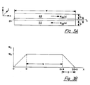
- FIG. 3 a diagrammatic cross section of bit structure 10 of Figure 2 parallel to word line 13 where the cross section view in Figure 3A shows ferromagnetic thin films 22 and 23 and separating film 24.
- This cross section is taken relatively far from either of juncture interconnections 11. Insulating layers, protective layers, semiconductor material body substrate and the like are ignored and therefore omitted from the cross section of Figure 3.
- Each of ferromagnetic thin films 22 and 23 are shown in Figure 3 to have a thickness designated T F while the separating film 24 which is free of any ferromagnetic properties is shown to have a thickness T S .
- the transverse operating mode has been chosen here, so that the easy axis in each film is parallel to word line 13.
- the magnetization shown for each film, M22(x) and M23(x) are both shown as a function of x for reasons to be described, and are shown in opposite directions along the x axis which is an arrangement that minimizes the magnetic energy.
- anisotropy fields are dominated by the demagnetizing fields due to the "free poles" at the edges. If the magnetizations of films 22 and 23 were saturated, the demagnetizing fields would approach M S /2 in the films or about 398 KA/m (5,000 Oersteds) for films with the alloys described here. Typical films of these alloys will have a coercitivity and an anisotropy field in the order of only 1,6 KA/m (20 Oersteds), leading to instabilities in the magnetization at the edges of these films.
- films with easy directions on the transverse axis do not truly saturate across the films. Further, films that are thicker or having greater separation therebetween, or both, are found to have even less of the central interior regions of the strip in magnetic saturation along the x axis leading to even less stability.
- the uncancelled field in one film that is, the magnetic field in one of films 22 and 23 due to the demagnetization fields in each of these films can be found from again using inscribed elipsoids in the x-y plane of the cross sections of films 22 and 23 in Figure 3 as a basis for such a determination.
- the uncancelled field in the chosen film can be found by finding the field at the midpoint of such a film because the average effect of field in the film can be approximated as the field occurring at such midpoint.
- These inscribed elipsoids have their major axes along the width of films 22 and 23 of a length equal to w or 2r.
- the magnetizations of the films are saturated inside these elipsoids.
- the center of one film is separated from the other by the distance T F + T S .
- H uncan H D g((T f + T s )/r), where H D is the demagnetizing field occurring within one of the elipsoids in one of the films due to just the surface poles of that film, and g, as a function of the argument (T f + T s )/r, is a cancellation factor arising because of the action of the demagnetizing field of the other film opposing the demagnetizing field of the first film.
- T f + T S is much less than r
- the uncancelled field has been found to satisfy the approximation: Experiment has confirmed the accuracy of this approximation.
- the value of the anisotropy magnetic field H K in ferromagnetic thin films of the nature being considered here is typically 0.8 to 2,4 kA/m (10 to 30 Oersteds) determined primarily by the chemical composition of the film but also depending on various other parameters such as angle and deposition of the film on the substrate, the substrate temperature, anisotropic strains resulting in the film, and the like.
- the uncancelled portions of the demagnetizing fields in the film should be kept in the range from 0,16 to 0,48 kA/m (2 to 6 Oersteds). That is, the ratio of H uncan to H K is a measure of the stability of the magnetization. The ratio is unacceptable with a value of 1 and one can be quite confident of a value of 10 so an intermediate ratio value such as 5 is a reasonable choice.
- values of permitted thin film thicknesses allowing stable magnetizations in films 22 and 23 in this design situation are of significance in illustrating the acceptable ranges of values. They can be obtained from this last inequality on assuming one of the thickness values. If the thickness of separating film 24 is chosen to have a thickness of 5 nm (50 ⁇ ), then the ferromagnetic films 22 and 23 must be less than about 10,5 nm (105 ⁇ ) in thickness.
- This thickness choice for separating film 24 is not an unreasonable choice in that the film needs only to be thick enough to break the exchange interaction coupling between electron spins in atoms at the edges of each of ferromagnetic film layers 22 and 23. Typically, a separation on the order of 1 nm (10 angstroms) is sufficient to eliminate such exchange coupling between layers 22 and 23.
- the material for layer 24 has been chosen to be an insulating film, silicon nitride, which gives good fabrication process results.
- the material in layer 24 could in some situations be either a ferromagnetic material or a ferrimagnetic material if there is sufficient exchange interaction mismatch with layers 22 and 23 to prevent the exchange interaction from coupling therebetween.
- the possible use of an outer magnetic material covering on the sides 26 could be eliminated as flux closure could be provided by this chosen material for layer 24.
- the thickness chosen for intermediate layer 24 is a reasonable one and leads to rather thin ferromagnetic films for layers 22 and 23 in this design example.
- the thickness of films 22 and 23 should be less than 30 nm (300 ⁇ ), and preferably less than 20 nm (200 ⁇ ).
- the thickness in these situations of intermediate layer 24 should be less than 10 nm (100 ⁇ ).
- Restricting the thickness of ferromagnetic films 22 and 23 sufficiently to achieve a relatively low uncancelled demagnetizing field in each is a good design practice because there may be further demagnetization fields arising in a practical design not accounted for in the foregoing analysis. For instance, there will be some demagnetizing fields occuring along the z axis in films 22 and 23 which would also be reduced by a restricted film thickness. Further, while films 22 and 23 have been shown to be of comparable thickness and width, this may not necessarily be the best design in each situation. Further, a different alloy material for each of films 22 and 23 may be desirable in some design situations. These sorts of differences may lead to additional demagnetizing field strengths which also would be reduced by limiting the thickness of such films.
- Bit structure 10 can very readily be provided in a monolithic integrated circuit chip. Because bit structure 10 is formed on insulating layer 21 and would have only insulating protective layers thereover, and because none of these layers are magnetically permeable, bit structure 10 can be designed without reference to the integrated circuit structure environment. Further, the interconnections between the digital memory and the remaining portions of the integrated circuits can be provided by the normal integrated circuit fabrication process steps for providing interconnections.
Landscapes
- Engineering & Computer Science (AREA)
- Computer Hardware Design (AREA)
- Semiconductor Memories (AREA)
- Hall/Mr Elements (AREA)
- Thin Magnetic Films (AREA)
- Mram Or Spin Memory Techniques (AREA)
Claims (9)
- Mémoire numérique à base de film mince ferromagnétique, aveca) une première structure de ligne de stockage ayant une première paire de bornes terminales de ligne de stockage (12) prévues pour conduire du courant électrique dans au moins un sens, lesdites bornes terminales de ligne de stockage ayant plusieurs structures de bit (10) reliées électriquement en série entre elles,chacune desdites structures de bit était reliée électriquement au niveau d'au moins une jonction de bit (11) à une autre structure de bit, chacune desdites structures de bit comportant au moins une structure comportant :a1) une couche intermédiaire (24) d'un type de matériau de séparation, ladite couche intermédiaire ayant deux surfaces principales sur des côtés opposés de celle-ci de telle sorte que lesdites surfaces principales sont séparées de moins de 10 nm dudit matériau de séparation tout en étant suffisamment séparé pour ledit type de matériau de séparation afin d'empêcher toute interaction d'échange par couplage à travers celui-ci, eta2) un film de mémoire (22, 23) sur chacune desdites surfaces principales de couche intermédiaire ledit film de mémoire étant d'une épaisseur inférieure à 30 nm et en matériau ferromagnétique anisotrope magnétorésistif ; etb) plusieurs structures de ligne de mot (13,14) possédant chacune une paire de bornes terminales de ligne de mot (14) prévues pour conduire du courant électrique dans au moins un sens, chaque paire desdites bornes terminales de ligne de mot possédant un conducteur électrique (13) relié électriquement entre elles et qui est séparé par une couche électriquement isolante (25) dudit film de mémoire (23) sur une desdites surfaces principales de ladite couche intermédiaire d'une desdites structures de bit (10) sélectionnée.
- Mémoire selon la revendication 1, caractérisée en ce qu'un axe facile de magnétisation dudit film de mémoire (22, 23) dans au moins une desdites structures de bit (10) est sensiblement parallèle à un axe de ladite couche intermédiaire (24) où ledit axe a un point d'extrémité au niveau de chaque jonction de bit (11).
- Mémoire selon la revendication 1, caractérisée en ce qu'un axe facile de magnétisation dudit film de mémoire (22, 23) dans au moins une desdites structures de bit (10) est sensiblement perpendiculaire à un axe de ladite couche intermédiaire (24) où ledit axe a un point d'extrémité au niveau de chaque jonction de bit (11).
- Mémoire selon l'une des revendications précédentes, caractérisée en ce que ledit film (22, 23) sur chacune desdites surfaces principales de ladite couche intermédiaire (24) d'au moins une desdites structures de bit (10) est disposé de telle sorte qu'il y a deux films séparés (22, 23) avec un desdits films séparés sur chacune desdites surfaces principales.
- Mémoire selon l'une des revendications précédentes, caractérisée en ce que ledit film de mémoire (22, 23) sur chacune desdites surfaces principales de ladite couche intermédiaire (24) d'au moins une desdites structures de bit (10) est disposé de telle sorte que le matériau ferromagnétique (22, 26, 23) entoure sensiblement ladite couche intermédiaire (24) au moins là où ladite structure de bit (10) est exempte d'une jonction de bit (11).
- Mémoire selon l'une des revendications précédentes, caractérisée en ce qu'au moins une deuxième structure de ligne de stockage est prévue sensiblement en correspondance avec ladite première structure de ligne de bit comprenant la relation structurelle avec lesdites structures de ligne de mot.
- Mémoire selon l'une des revendications précédentes, caractérisée en ce que ledit film de mémoire (22, 23) sur lesdites surfaces principales de ladite couche intermédiaire (24) de chacune desdites structures de bit (10) est d'une épaisseur inférieure à 20 nm.
- Mémoire selon l'une des revendications précédentes, caractérisée en ce que la couche intermédiaire (24) se compose de nitrure de silicium.
- Mémoire selon l'une des revendications 1 à 7, caractérisée en ce que la couche intermédiaire se compose d'un matériau ferromagnétique ou ferrimagnétique.
Applications Claiming Priority (2)
| Application Number | Priority Date | Filing Date | Title |
|---|---|---|---|
| US06/870,068 US4780848A (en) | 1986-06-03 | 1986-06-03 | Magnetoresistive memory with multi-layer storage cells having layers of limited thickness |
| US870068 | 1986-06-03 |
Publications (3)
| Publication Number | Publication Date |
|---|---|
| EP0248355A2 EP0248355A2 (fr) | 1987-12-09 |
| EP0248355A3 EP0248355A3 (en) | 1990-03-28 |
| EP0248355B1 true EP0248355B1 (fr) | 1992-04-08 |
Family
ID=25354735
Family Applications (1)
| Application Number | Title | Priority Date | Filing Date |
|---|---|---|---|
| EP87107788A Expired EP0248355B1 (fr) | 1986-06-03 | 1987-05-29 | Mémoire magnétique |
Country Status (5)
| Country | Link |
|---|---|
| US (1) | US4780848A (fr) |
| EP (1) | EP0248355B1 (fr) |
| JP (1) | JPS6342089A (fr) |
| CA (1) | CA1284382C (fr) |
| DE (1) | DE3778065D1 (fr) |
Families Citing this family (71)
| Publication number | Priority date | Publication date | Assignee | Title |
|---|---|---|---|---|
| US4945397A (en) * | 1986-12-08 | 1990-07-31 | Honeywell Inc. | Resistive overlayer for magnetic films |
| US4897288A (en) * | 1987-01-28 | 1990-01-30 | Honeywell Inc. | Vialess shorting bars for magnetoresistive devices |
| US4918655A (en) * | 1988-02-29 | 1990-04-17 | Honeywell Inc. | Magnetic device integrated circuit interconnection system |
| EP0356093B1 (fr) * | 1988-08-12 | 1993-03-31 | Nissin Shokuhin Kabushiki Kaisha | Conteneur autochauffant |
| AU641635B2 (en) * | 1989-02-22 | 1993-09-30 | Nissin Shokuhin Kabushiki Kaisha | Ignition system and self-heating container |
| US5039655A (en) * | 1989-07-28 | 1991-08-13 | Ampex Corporation | Thin film memory device having superconductor keeper for eliminating magnetic domain creep |
| US5012444A (en) * | 1990-04-04 | 1991-04-30 | Honeywell Inc. | Opposed field magnetoresistive memory sensing |
| US5060193A (en) * | 1990-04-04 | 1991-10-22 | Honeywell Inc. | Magnetic state entry assurance |
| US5390061A (en) | 1990-06-08 | 1995-02-14 | Hitachi, Ltd. | Multilayer magnetoresistance effect-type magnetic head |
| CA2060835A1 (fr) * | 1991-02-11 | 1992-08-12 | Romney R. Katti | Memoire vive analogique rapide remanente en circuit integre |
| US5251170A (en) * | 1991-11-04 | 1993-10-05 | Nonvolatile Electronics, Incorporated | Offset magnetoresistive memory structures |
| US5247278A (en) * | 1991-11-26 | 1993-09-21 | Honeywell Inc. | Magnetic field sensing device |
| US5420819A (en) * | 1992-09-24 | 1995-05-30 | Nonvolatile Electronics, Incorporated | Method for sensing data in a magnetoresistive memory using large fractions of memory cell films for data storage |
| US5477482A (en) * | 1993-10-01 | 1995-12-19 | The United States Of America As Represented By The Secretary Of The Navy | Ultra high density, non-volatile ferromagnetic random access memory |
| US5515314A (en) * | 1994-05-27 | 1996-05-07 | Fujitsu Limited | Storage device |
| US5587943A (en) * | 1995-02-13 | 1996-12-24 | Integrated Microtransducer Electronics Corporation | Nonvolatile magnetoresistive memory with fully closed flux operation |
| US6741494B2 (en) * | 1995-04-21 | 2004-05-25 | Mark B. Johnson | Magnetoelectronic memory element with inductively coupled write wires |
| US7050329B2 (en) * | 1995-04-21 | 2006-05-23 | Johnson Mark B | Magnetic spin based memory with inductive write lines |
| US5702831A (en) * | 1995-11-06 | 1997-12-30 | Motorola | Ferromagnetic GMR material |
| US5659499A (en) * | 1995-11-24 | 1997-08-19 | Motorola | Magnetic memory and method therefor |
| US5756366A (en) * | 1995-12-21 | 1998-05-26 | Honeywell Inc. | Magnetic hardening of bit edges of magnetoresistive RAM |
| US5569617A (en) * | 1995-12-21 | 1996-10-29 | Honeywell Inc. | Method of making integrated spacer for magnetoresistive RAM |
| US5745408A (en) * | 1996-09-09 | 1998-04-28 | Motorola, Inc. | Multi-layer magnetic memory cell with low switching current |
| US6048739A (en) * | 1997-12-18 | 2000-04-11 | Honeywell Inc. | Method of manufacturing a high density magnetic memory device |
| US5956267A (en) * | 1997-12-18 | 1999-09-21 | Honeywell Inc | Self-aligned wordline keeper and method of manufacture therefor |
| US20040017721A1 (en) * | 1998-10-30 | 2004-01-29 | Schwabe Nikolai Franz Gregoe | Magnetic storage device |
| GB2343308B (en) * | 1998-10-30 | 2000-10-11 | Nikolai Franz Gregor Schwabe | Magnetic storage device |
| US6872993B1 (en) | 1999-05-25 | 2005-03-29 | Micron Technology, Inc. | Thin film memory device having local and external magnetic shielding |
| WO2000079540A1 (fr) * | 1999-06-18 | 2000-12-28 | Nve Corporation | Stockage de donnees par impulsions thermiques coincidant avec une memoire magnetique |
| US6317359B1 (en) | 1999-07-07 | 2001-11-13 | Iowa State University Research Foundation, Inc. | Non-volatile magnetic circuit |
| US6343032B1 (en) | 1999-07-07 | 2002-01-29 | Iowa State University Research Foundation, Inc. | Non-volatile spin dependent tunnel junction circuit |
| US6542000B1 (en) | 1999-07-30 | 2003-04-01 | Iowa State University Research Foundation, Inc. | Nonvolatile programmable logic devices |
| US6611405B1 (en) * | 1999-09-16 | 2003-08-26 | Kabushiki Kaisha Toshiba | Magnetoresistive element and magnetic memory device |
| US6285581B1 (en) | 1999-12-13 | 2001-09-04 | Motorola, Inc. | MRAM having semiconductor device integrated therein |
| US6392922B1 (en) * | 2000-08-14 | 2002-05-21 | Micron Technology, Inc. | Passivated magneto-resistive bit structure and passivation method therefor |
| US6413788B1 (en) | 2001-02-28 | 2002-07-02 | Micron Technology, Inc. | Keepers for MRAM electrodes |
| JP2002298588A (ja) * | 2001-03-30 | 2002-10-11 | Fujitsu Ltd | 半導体装置及びその検査方法 |
| US6744086B2 (en) | 2001-05-15 | 2004-06-01 | Nve Corporation | Current switched magnetoresistive memory cell |
| DE10128964B4 (de) * | 2001-06-15 | 2012-02-09 | Qimonda Ag | Digitale magnetische Speicherzelleneinrichtung |
| US6693826B1 (en) | 2001-07-30 | 2004-02-17 | Iowa State University Research Foundation, Inc. | Magnetic memory sensing method and apparatus |
| US6500676B1 (en) | 2001-08-20 | 2002-12-31 | Honeywell International Inc. | Methods and apparatus for depositing magnetic films |
| US6510080B1 (en) | 2001-08-28 | 2003-01-21 | Micron Technology Inc. | Three terminal magnetic random access memory |
| US6485989B1 (en) | 2001-08-30 | 2002-11-26 | Micron Technology, Inc. | MRAM sense layer isolation |
| US6545906B1 (en) | 2001-10-16 | 2003-04-08 | Motorola, Inc. | Method of writing to scalable magnetoresistance random access memory element |
| US6717194B2 (en) * | 2001-10-30 | 2004-04-06 | Micron Technology, Inc. | Magneto-resistive bit structure and method of manufacture therefor |
| US6829157B2 (en) * | 2001-12-05 | 2004-12-07 | Korea Institute Of Science And Technology | Method of controlling magnetization easy axis in ferromagnetic films using voltage, ultrahigh-density, low power, nonvolatile magnetic memory using the control method, and method of writing information on the magnetic memory |
| AU2003225048A1 (en) * | 2002-04-19 | 2003-11-03 | Integrated Magnetoelectronics Corporation | Interfaces between semiconductor circuitry and transpinnor-based circuitry |
| US6783995B2 (en) * | 2002-04-30 | 2004-08-31 | Micron Technology, Inc. | Protective layers for MRAM devices |
| US6724652B2 (en) * | 2002-05-02 | 2004-04-20 | Micron Technology, Inc. | Low remanence flux concentrator for MRAM devices |
| US6744663B2 (en) * | 2002-06-28 | 2004-06-01 | Motorola, Inc. | Circuit and method for reading a toggle memory cell |
| US6806523B2 (en) * | 2002-07-15 | 2004-10-19 | Micron Technology, Inc. | Magnetoresistive memory devices |
| US7095646B2 (en) | 2002-07-17 | 2006-08-22 | Freescale Semiconductor, Inc. | Multi-state magnetoresistance random access cell with improved memory storage density |
| US6914805B2 (en) * | 2002-08-21 | 2005-07-05 | Micron Technology, Inc. | Method for building a magnetic keeper or flux concentrator used for writing magnetic bits on a MRAM device |
| KR100515053B1 (ko) * | 2002-10-02 | 2005-09-14 | 삼성전자주식회사 | 비트라인 클램핑 전압 레벨에 대해 안정적인 독출 동작이가능한 마그네틱 메모리 장치 |
| US7023723B2 (en) * | 2002-11-12 | 2006-04-04 | Nve Corporation | Magnetic memory layers thermal pulse transitions |
| US6992919B2 (en) * | 2002-12-20 | 2006-01-31 | Integrated Magnetoelectronics Corporation | All-metal three-dimensional circuits and memories |
| US6765823B1 (en) * | 2003-01-29 | 2004-07-20 | Micron Technology Incorporated | Magnetic memory cell with shape anisotropy |
| US7002228B2 (en) * | 2003-02-18 | 2006-02-21 | Micron Technology, Inc. | Diffusion barrier for improving the thermal stability of MRAM devices |
| US7005852B2 (en) | 2003-04-04 | 2006-02-28 | Integrated Magnetoelectronics Corporation | Displays with all-metal electronics |
| EP1639656B1 (fr) * | 2003-06-23 | 2019-06-12 | NVE Corporation | Cellule de memoire ferromagnetique regle thermiquement |
| US6956763B2 (en) | 2003-06-27 | 2005-10-18 | Freescale Semiconductor, Inc. | MRAM element and methods for writing the MRAM element |
| US6967366B2 (en) | 2003-08-25 | 2005-11-22 | Freescale Semiconductor, Inc. | Magnetoresistive random access memory with reduced switching field variation |
| US7078239B2 (en) * | 2003-09-05 | 2006-07-18 | Micron Technology, Inc. | Integrated circuit structure formed by damascene process |
| US7112454B2 (en) * | 2003-10-14 | 2006-09-26 | Micron Technology, Inc. | System and method for reducing shorting in memory cells |
| US20050106359A1 (en) * | 2003-11-13 | 2005-05-19 | Honeywell International Inc. | Method of processing substrate |
| US7072209B2 (en) * | 2003-12-29 | 2006-07-04 | Micron Technology, Inc. | Magnetic memory having synthetic antiferromagnetic pinned layer |
| US7148531B2 (en) * | 2004-04-29 | 2006-12-12 | Nve Corporation | Magnetoresistive memory SOI cell |
| WO2006044244A2 (fr) * | 2004-10-12 | 2006-04-27 | Nve Corporataion | Memoire de commutation a transfert de moment de spin a assistance thermomagnetique |
| US7129098B2 (en) | 2004-11-24 | 2006-10-31 | Freescale Semiconductor, Inc. | Reduced power magnetoresistive random access memory elements |
| US7911830B2 (en) * | 2007-05-17 | 2011-03-22 | Integrated Magnetoelectronics | Scalable nonvolatile memory |
| US9741923B2 (en) | 2015-09-25 | 2017-08-22 | Integrated Magnetoelectronics Corporation | SpinRAM |
Family Cites Families (15)
| Publication number | Priority date | Publication date | Assignee | Title |
|---|---|---|---|---|
| NL258618A (fr) * | 1960-12-01 | |||
| BE620452A (fr) * | 1961-07-20 | |||
| NL6401805A (fr) * | 1964-02-26 | 1965-08-27 | ||
| FR1456686A (fr) * | 1964-08-10 | 1966-07-08 | Toko Inc | Mémoire magnétique perfectionnée par absorption des déformations des fils magnétiques minces supprimant les distorsions magnétiques |
| GB1059310A (en) * | 1965-04-27 | 1967-02-15 | Mullard Ltd | Improvements in or relating to depositing conductive magnetic material on to a non-conductive substrate |
| US3423739A (en) * | 1965-08-16 | 1969-01-21 | Sperry Rand Corp | Nondestructive read memory selection system |
| US3493943A (en) * | 1965-10-05 | 1970-02-03 | Massachusetts Inst Technology | Magnetoresistive associative memory |
| DE1922552A1 (de) * | 1969-05-02 | 1970-11-19 | Siemens Ag | Magnetschichtspeicherzelle mit geschlossenem magnetischen Kreis in Richtung leichter Magnetisierbarkeit der Speicherschichten und Verfahren zur Herstellung |
| US3883858A (en) * | 1973-12-17 | 1975-05-13 | Ampex | Magnetoresistive readout transducer for sensing magnetic domains in thin film memories |
| FR2276658A1 (fr) * | 1974-06-25 | 1976-01-23 | Tecsi | Poste de lecture pour un registre a propagation de domaines magnetiques sur une couche mince |
| US4208725A (en) * | 1979-02-23 | 1980-06-17 | Sperry Corporation | Magneto-resistive detector for cross-tie wall memory system |
| US4356523A (en) * | 1980-06-09 | 1982-10-26 | Ampex Corporation | Narrow track magnetoresistive transducer assembly |
| JPS5999370A (ja) * | 1982-11-30 | 1984-06-08 | Copal Co Ltd | 磁気抵抗素子を具える磁気検出器の製造方法 |
| US4455626A (en) * | 1983-03-21 | 1984-06-19 | Honeywell Inc. | Thin film memory with magnetoresistive read-out |
| US4639806A (en) * | 1983-09-09 | 1987-01-27 | Sharp Kabushiki Kaisha | Thin film magnetic head having a magnetized ferromagnetic film on the MR element |
-
1986
- 1986-06-03 US US06/870,068 patent/US4780848A/en not_active Expired - Lifetime
-
1987
- 1987-05-29 EP EP87107788A patent/EP0248355B1/fr not_active Expired
- 1987-05-29 DE DE8787107788T patent/DE3778065D1/de not_active Expired - Lifetime
- 1987-05-29 JP JP62134734A patent/JPS6342089A/ja active Granted
- 1987-06-02 CA CA000538580A patent/CA1284382C/fr not_active Expired - Lifetime
Also Published As
| Publication number | Publication date |
|---|---|
| JPH0444352B2 (fr) | 1992-07-21 |
| EP0248355A2 (fr) | 1987-12-09 |
| DE3778065D1 (de) | 1992-05-14 |
| JPS6342089A (ja) | 1988-02-23 |
| US4780848A (en) | 1988-10-25 |
| EP0248355A3 (en) | 1990-03-28 |
| CA1284382C (fr) | 1991-05-21 |
Similar Documents
| Publication | Publication Date | Title |
|---|---|---|
| EP0248355B1 (fr) | Mémoire magnétique | |
| US4731757A (en) | Magnetoresistive memory including thin film storage cells having tapered ends | |
| US5595830A (en) | Magnetoresistive structure with alloy layer having two substantially immiscible components | |
| US5569544A (en) | Magnetoresistive structure comprising ferromagnetic thin films and intermediate layers of less than 30 angstroms formed of alloys having immiscible components | |
| US5251170A (en) | Offset magnetoresistive memory structures | |
| US5617071A (en) | Magnetoresistive structure comprising ferromagnetic thin films and intermediate alloy layer having magnetic concentrator and shielding permeable masses | |
| EP1244117B1 (fr) | Elément magnétorésistif,élément de mémoire utilisant cet élément magnétorésistif,et méthode pour enregistrement/reproduction pour cet élément de mémoire | |
| Daughton | Magnetoresistive memory technology | |
| US4751677A (en) | Differential arrangement magnetic memory cell | |
| EP0710390B1 (fr) | Structure magnetique avec des couches stratifiees | |
| EP0937302B1 (fr) | Memoire a effet tunnel dependant du spin magnetique | |
| US6349053B1 (en) | Spin dependent tunneling memory | |
| EP1151482B1 (fr) | Capteur a effet tunnel dependant du spin | |
| US7390584B2 (en) | Spin dependent tunneling devices having reduced topological coupling | |
| US20020171100A1 (en) | Circuit selected joint magnetoresistive junction tunneling-giant magnetoresistive effects memory cells | |
| EP2447947B1 (fr) | Memoire a effet tunnel dependant du spin | |
| JPH077593B2 (ja) | 磁気記憶素子 |
Legal Events
| Date | Code | Title | Description |
|---|---|---|---|
| PUAI | Public reference made under article 153(3) epc to a published international application that has entered the european phase |
Free format text: ORIGINAL CODE: 0009012 |
|
| AK | Designated contracting states |
Kind code of ref document: A2 Designated state(s): DE FR GB IT NL |
|
| PUAL | Search report despatched |
Free format text: ORIGINAL CODE: 0009013 |
|
| AK | Designated contracting states |
Kind code of ref document: A3 Designated state(s): DE FR GB IT NL |
|
| RHK1 | Main classification (correction) |
Ipc: G11C 11/15 |
|
| 17P | Request for examination filed |
Effective date: 19900917 |
|
| 17Q | First examination report despatched |
Effective date: 19910619 |
|
| GRAA | (expected) grant |
Free format text: ORIGINAL CODE: 0009210 |
|
| AK | Designated contracting states |
Kind code of ref document: B1 Designated state(s): DE FR GB IT NL |
|
| REF | Corresponds to: |
Ref document number: 3778065 Country of ref document: DE Date of ref document: 19920514 |
|
| ITTA | It: last paid annual fee | ||
| ET | Fr: translation filed | ||
| ITF | It: translation for a ep patent filed | ||
| PLBE | No opposition filed within time limit |
Free format text: ORIGINAL CODE: 0009261 |
|
| STAA | Information on the status of an ep patent application or granted ep patent |
Free format text: STATUS: NO OPPOSITION FILED WITHIN TIME LIMIT |
|
| 26N | No opposition filed | ||
| PGFP | Annual fee paid to national office [announced via postgrant information from national office to epo] |
Ref country code: FR Payment date: 20010529 Year of fee payment: 15 |
|
| PGFP | Annual fee paid to national office [announced via postgrant information from national office to epo] |
Ref country code: NL Payment date: 20010531 Year of fee payment: 15 |
|
| REG | Reference to a national code |
Ref country code: GB Ref legal event code: IF02 |
|
| PG25 | Lapsed in a contracting state [announced via postgrant information from national office to epo] |
Ref country code: NL Free format text: LAPSE BECAUSE OF NON-PAYMENT OF DUE FEES Effective date: 20021201 |
|
| PG25 | Lapsed in a contracting state [announced via postgrant information from national office to epo] |
Ref country code: FR Free format text: LAPSE BECAUSE OF NON-PAYMENT OF DUE FEES Effective date: 20030131 |
|
| NLV4 | Nl: lapsed or anulled due to non-payment of the annual fee |
Effective date: 20021201 |
|
| REG | Reference to a national code |
Ref country code: FR Ref legal event code: ST |
|
| REG | Reference to a national code |
Ref country code: FR Ref legal event code: TP |
|
| REG | Reference to a national code |
Ref country code: GB Ref legal event code: 732E |
|
| PG25 | Lapsed in a contracting state [announced via postgrant information from national office to epo] |
Ref country code: IT Free format text: LAPSE BECAUSE OF NON-PAYMENT OF DUE FEES;WARNING: LAPSES OF ITALIAN PATENTS WITH EFFECTIVE DATE BEFORE 2007 MAY HAVE OCCURRED AT ANY TIME BEFORE 2007. THE CORRECT EFFECTIVE DATE MAY BE DIFFERENT FROM THE ONE RECORDED. Effective date: 20050529 |
|
| PGFP | Annual fee paid to national office [announced via postgrant information from national office to epo] |
Ref country code: GB Payment date: 20060524 Year of fee payment: 20 |
|
| PGFP | Annual fee paid to national office [announced via postgrant information from national office to epo] |
Ref country code: DE Payment date: 20060525 Year of fee payment: 20 |
|
| REG | Reference to a national code |
Ref country code: GB Ref legal event code: PE20 |
|
| PG25 | Lapsed in a contracting state [announced via postgrant information from national office to epo] |
Ref country code: GB Free format text: LAPSE BECAUSE OF EXPIRATION OF PROTECTION Effective date: 20070528 |