EP0249733A1 - Synthétiseur de fréquence - Google Patents
Synthétiseur de fréquence Download PDFInfo
- Publication number
- EP0249733A1 EP0249733A1 EP87106623A EP87106623A EP0249733A1 EP 0249733 A1 EP0249733 A1 EP 0249733A1 EP 87106623 A EP87106623 A EP 87106623A EP 87106623 A EP87106623 A EP 87106623A EP 0249733 A1 EP0249733 A1 EP 0249733A1
- Authority
- EP
- European Patent Office
- Prior art keywords
- frequency
- signal
- signals
- input
- switched
- Prior art date
- Legal status (The legal status is an assumption and is not a legal conclusion. Google has not performed a legal analysis and makes no representation as to the accuracy of the status listed.)
- Granted
Links
- 238000011144 upstream manufacturing Methods 0.000 claims description 3
- 230000001360 synchronised effect Effects 0.000 claims description 2
- 230000000717 retained effect Effects 0.000 claims 1
- 238000010586 diagram Methods 0.000 description 5
- 230000015572 biosynthetic process Effects 0.000 description 1
- 230000000694 effects Effects 0.000 description 1
- 230000007774 longterm Effects 0.000 description 1
- 238000000034 method Methods 0.000 description 1
- 230000010355 oscillation Effects 0.000 description 1
- 238000003786 synthesis reaction Methods 0.000 description 1
- 230000029305 taxis Effects 0.000 description 1
Images

Classifications
-
- H—ELECTRICITY
- H03—ELECTRONIC CIRCUITRY
- H03B—GENERATION OF OSCILLATIONS, DIRECTLY OR BY FREQUENCY-CHANGING, BY CIRCUITS EMPLOYING ACTIVE ELEMENTS WHICH OPERATE IN A NON-SWITCHING MANNER; GENERATION OF NOISE BY SUCH CIRCUITS
- H03B21/00—Generation of oscillations by combining unmodulated signals of different frequencies
- H03B21/01—Generation of oscillations by combining unmodulated signals of different frequencies by beating unmodulated signals of different frequencies
- H03B21/02—Generation of oscillations by combining unmodulated signals of different frequencies by beating unmodulated signals of different frequencies by plural beating, i.e. for frequency synthesis ; Beating in combination with multiplication or division of frequency
Definitions
- the present invention relates to a frequency synthesizer according to the preamble of claim 1.
- the invention is therefore based on the object of generating an output signal in such an arrangement which is phase-coherent even in the case of frequency switching. This object is achieved by the measures set out in the characterizing part of patent claim 1. Advantageous embodiments of the invention are specified in further claims.
- the frequency synthesizer according to FIG. 1 comprises a switching device US, two frequency divider circuits TS1, TS2 and two mixers M1, M2, each of which is followed by a filter F1 or F2.
- the switching device US has four inputs for a signal S1, S2, S3, S4 of frequency f1, f2, f3 or f4 and three outputs for a signal Sx, Sy, Sz of frequency fx, fy or fz.
- the signal Sx is passed through the frequency divider circuit TS1 and mixed in the mixer M1 with the signal Sy.
- the output signal Sw of the filter F1 is passed through the frequency divider circuit TS2 and mixed in the mixer M2 with the signal Sz, a frequency divider circuit, a mixer and a filter each forming a mixer stage.
- a signal S ⁇ o of frequency f ⁇ o appears, which in itself corresponds to the frequency of a frequency synthesizer according to the prior art.
- the frequency divider circuits TS1 and TS2 have a switch L1 or L2 actuated by the output signal Sk of a control circuit KS via an OR gate G1 or G2, to which a frequency divider T1 or T2 is connected .
- the other input of the OR gate G1 or G2 is acted upon by the output signal of the frequency divider T1 or T2.
- the circuit KS can be, for example, a JK or D flip-flop, the clock input of which is supplied with a signal Sgt and the preset input of which is supplied with a signal Sm which has the value "1" as long as the code signals Sc are valid, which are the switching device US taxes.
- the described part of the frequency synthesizer according to the invention according to FIG. 1 can be expanded such that the switching device US supplies an additional signal Su, the frequency fu of which can also be one of the frequencies f1, f2, f3 or f4.
- the signal Su is mixed with another signal SU and, via the series connection of a bandpass filter FU and a frequency multiplier V, is fed to the input of a further mixer M3, which mixes this signal with the output signal S ⁇ o of the filter F2.
- the mixer M3 is followed by a bandpass filter F3, from which the useful signal S ⁇ o of the frequency f ⁇ o is taken. Since the extended frequency synthesizer has no further frequency divider, but only a frequency multiplier V, the useful signal S ⁇ o does not lose the phase coherence obtained by the control circuit KS.
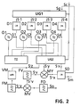
- the frequency synthesizer according to FIG. 2 comprises a switching device consisting of two interconnecting switchers UG1 and UG2, four frequency dividers D1, D2, D3, D4, a frequency multiplier VM with a downstream filter FM and two mixers MY and MV, each of which has a filter FV or FO is connected downstream.
- the switching element UG2 has four inputs for a signal S1, S2, S3, S4 of the frequency f1, f2, f3 or f4 and two outputs for a signal S ⁇ y, S ⁇ z of the frequency fy, fz.
- the signals S1, S2, S3 and S4 generated, for example, by an oscillator O1, O2, O3 or O4 are each fed via one of the frequency dividers D1, D2, D3, D4 to one input of the switching element UG1, which generates a signal Sg of the frequency f ⁇ x delivers.
- the four oscillators O1, O2, O3, O4 are, for example, synchronized together by a clock center TZ.
- FIG. 2 also shows an optional frequency divider circuit SD, the function of which will be explained later.
- the output signal S ⁇ x of the frequency divider circuit SD is mixed with the signal S ⁇ y in the mixer MY, the output of which is connected via the filter FV to the first input of the mixer MV.
- the signal S ⁇ z is fed via the elements VM and FM to the second input of the mixer MV, the filtered output signal So of which is a phase-coherent useful signal.
- the frequency synthesizer according to FIG. 2 without the divider circuit SD functions as follows:
- the signals Sg and S ⁇ x are the same.
- the switching elements UG1 and UG2 are designed such that the signal Sg is either one of the signals S ⁇ 1, S ⁇ 2, S ⁇ 3 or S ⁇ 4 at the outputs of the dividers D1, D2, D3 or D4 and the signals S ⁇ y and S ⁇ z are either one of the signals S1, S2, S3 or S4.
- phase rigidity of the signals S1, S2, S3 and S4 with one another can also be achieved by other means, for example using a single oscillator and three or four frequency dividers or using two oscillators and two frequency dividers.
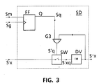
- a flip-flop FF whose output Q is connected via an OR gate G3 to the control input of a switch SW which interrupts the current path for a signal S ⁇ x sum input of a divider DV, the output of which is connected to the other input of the gate G3 is connected.
- the signal input of the flip-flop FF is supplied with the control signal Sm and its clock input with the signal Sg.
- the signal S ⁇ x can be taken from the output of the divider DV.
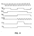
- the 4 shows time diagrams for the signals S ⁇ x, Sg, Sm and S ⁇ x and for three further signals Sq, S ⁇ q and S ⁇ xq.
- the signals Sq and S ⁇ q are the output signals of the flip-flop FF (Fig. 3) and the gate G3.
- the signal S ⁇ xq the input signal of the divider DV.
- the switch SW closes with the active edge of the signal Sg after the appearance of a signal Sm with the value "1".
- the switching element UG2 has an additional output for the signal S ⁇ x, which is therefore also a switched signal of the frequency f1, f2, f3 or f4.
- the signal Sq at the output of the flip-flop FF begins exactly with the active edge of the signal Sg (FIG. 4)
- the signal S ⁇ x arrives at the divider DV exactly when and only when a multiple of n oscillations of the signal S'x has already passed through.
- the signals S ⁇ x and S ⁇ x are always phase-coherent, even if the signal S ⁇ x is interrupted and switched through again.
- the signals S ⁇ y and S ⁇ z are also phase-coherent, this also applies to the signal So.
- the multiplier VM and the elements FM, MV and FO can be omitted with a suitable shift of the oscillator frequencies, which is less expensive Realization corresponds. Since there is normally also a switch for switching the signal SGx in the switching element UG2, this switch can take over the function of the switch SW (FIG. 3).
- the divider circuit SD could be a divider of the usual type; however, the signal S ⁇ q would have to control the switching element UG2 together with the switching code signal Sc.
- the dividers T1 and T2 (FIG. 1) and the divider DV (FIG. 3) are preferably dividers that divide by four. Such a divider consists of a certain number of flip-flops that cannot be reset because they have no reset input. In the event of a frequency change, the divider must still remain sufficiently active until the output signal Sk (FIG. 1) or S 1x (FIG. 3) has a constant value. This is achieved in that the signal Sk or Sq is combined with the output signal of the divider T1 or T2 or DV through the OR gates G1, G2 or G3.
- the switches L1, L2 and DV are thus controlled by output signals from the gates G1, G2 and G3.
- the signal Sg is thus decisive for the switch control when switching on and when the signal S ⁇ x is switched off. However, it should be noted that there is an additional time delay.
- the switching device US according to FIG. 1 and the switching elements UG1 and UG2 according to FIG. 2 preferably contain high-quality switching elements in analog technology, such as so-called 4PST switches.
- a commercially available one-of-four demultiplexer can be provided for the switching element UG1.
Landscapes
- Stabilization Of Oscillater, Synchronisation, Frequency Synthesizers (AREA)
Applications Claiming Priority (4)
| Application Number | Priority Date | Filing Date | Title |
|---|---|---|---|
| CH2337/86 | 1986-06-10 | ||
| CH233786 | 1986-06-10 | ||
| CH1355/87 | 1987-04-08 | ||
| CH135587 | 1987-04-08 |
Publications (2)
| Publication Number | Publication Date |
|---|---|
| EP0249733A1 true EP0249733A1 (fr) | 1987-12-23 |
| EP0249733B1 EP0249733B1 (fr) | 1992-07-22 |
Family
ID=25687428
Family Applications (1)
| Application Number | Title | Priority Date | Filing Date |
|---|---|---|---|
| EP19870106623 Expired - Lifetime EP0249733B1 (fr) | 1986-06-10 | 1987-05-07 | Synthétiseur de fréquence |
Country Status (2)
| Country | Link |
|---|---|
| EP (1) | EP0249733B1 (fr) |
| DE (1) | DE3780519D1 (fr) |
Citations (3)
| Publication number | Priority date | Publication date | Assignee | Title |
|---|---|---|---|---|
| GB1037583A (en) * | 1964-03-25 | 1966-07-27 | Communications Patents Ltd | Improvements in or relating to variable frequency oscillation generators |
| US3331035A (en) * | 1965-08-23 | 1967-07-11 | Sanders Associates Inc | Frequency synthesizer |
| FR2554292A1 (fr) * | 1983-10-31 | 1985-05-03 | Anritsu Electric Co Ltd | Generateur de signal |
-
1987
- 1987-05-07 EP EP19870106623 patent/EP0249733B1/fr not_active Expired - Lifetime
- 1987-05-07 DE DE8787106623T patent/DE3780519D1/de not_active Expired - Fee Related
Patent Citations (3)
| Publication number | Priority date | Publication date | Assignee | Title |
|---|---|---|---|---|
| GB1037583A (en) * | 1964-03-25 | 1966-07-27 | Communications Patents Ltd | Improvements in or relating to variable frequency oscillation generators |
| US3331035A (en) * | 1965-08-23 | 1967-07-11 | Sanders Associates Inc | Frequency synthesizer |
| FR2554292A1 (fr) * | 1983-10-31 | 1985-05-03 | Anritsu Electric Co Ltd | Generateur de signal |
Non-Patent Citations (1)
| Title |
|---|
| IEEE TRANSACTIONS ON MICROWAVE THEORY AND TECHNIQUES, Band MTT-30, Nr. 5, Mai 1982, Seiten 686-693, New York, US; A.J. BUDREAU et al.: "A review of SAW-based direct frequency synthesizers" * |
Also Published As
| Publication number | Publication date |
|---|---|
| DE3780519D1 (de) | 1992-08-27 |
| EP0249733B1 (fr) | 1992-07-22 |
Similar Documents
| Publication | Publication Date | Title |
|---|---|---|
| DE69415897T2 (de) | Frequenzsynthetisierer mit digitalem Phasenregelkreis, der einen Frequenzteiler mit rationalem Teilungsverhältnis enthält | |
| EP0012899B1 (fr) | Circuit de réglage de phase numérique avec un circuit auxiliaire | |
| DE102007042070B3 (de) | Spread-Spectrum-Taktung in Fraktional-N-PLLs | |
| DE2744432A1 (de) | Phasen- oder frequenzsteuerkreis im rueckkopplungskreis des oszillators eines fernseh-kanalwaehlers o.dgl. | |
| DE69423126T2 (de) | Mehrschleifenphasenregelkreis, FM-Empfangsverfahren und FM-Empfänger mit einem derartigen Phasenregelkreis | |
| DE69309838T2 (de) | Überlagerungsoszillator und Frequenzschaltverfahren dazu | |
| DE69300291T2 (de) | Frequenzregelschleife. | |
| DE2515969B2 (de) | Mehrkanalgenerator | |
| DE69922584T2 (de) | Hochfrequenzumsetzer | |
| DE3301991C2 (de) | Synchronisiersignal-Erzeugungseinrichtung | |
| DE3836814A1 (de) | Frequenzsynthesizer | |
| DE19630335A1 (de) | Phasensynchronisierter Oszillator für die Mikrowellen/Millimeterwellen-Bereiche | |
| DE2329381A1 (de) | Schwingungsgenerator | |
| DE2826098A1 (de) | Frequenzsyntheseschaltung | |
| EP0249733B1 (fr) | Synthétiseur de fréquence | |
| DE2149128C3 (de) | Verfahren zur Frequenzsynthese und Schaltungsanordnung zur Ausführung des Verfahrens | |
| EP0230337B1 (fr) | Arrangement de circuit pour la division de fréquence | |
| EP0025876A1 (fr) | Radiotéléphone à plusieurs canaux | |
| DE2816077C2 (de) | Frequenzgenerator | |
| DE2852029A1 (de) | Ueberlagerungsoszillator | |
| CH669075A5 (en) | Frequency synthesiser with mixers and phase-synchronised oscillators - multiplies and filters frequency of prodn. from mixer of selected outputs from externally coded switching circuit | |
| DE3201039A1 (de) | "oszillatorschaltung fuer ein wenigkanal-funkgeraet" | |
| EP0273203B1 (fr) | Synthétiseur de fréquence | |
| EP1347578B1 (fr) | Architecture d'horloge et dispositif d'horloge pour circuit intégré monolithique | |
| DE1591722C3 (de) | Frequenzaufbereitung nach dem Prinzip des digitalen Zählverfahrens |
Legal Events
| Date | Code | Title | Description |
|---|---|---|---|
| PUAI | Public reference made under article 153(3) epc to a published international application that has entered the european phase |
Free format text: ORIGINAL CODE: 0009012 |
|
| 17P | Request for examination filed |
Effective date: 19870518 |
|
| AK | Designated contracting states |
Kind code of ref document: A1 Designated state(s): CH DE FR GB IT LI NL SE |
|
| 17Q | First examination report despatched |
Effective date: 19900720 |
|
| GRAA | (expected) grant |
Free format text: ORIGINAL CODE: 0009210 |
|
| AK | Designated contracting states |
Kind code of ref document: B1 Designated state(s): CH DE FR GB IT LI NL SE |
|
| REF | Corresponds to: |
Ref document number: 3780519 Country of ref document: DE Date of ref document: 19920827 |
|
| GBT | Gb: translation of ep patent filed (gb section 77(6)(a)/1977) | ||
| ITF | It: translation for a ep patent filed | ||
| ET | Fr: translation filed | ||
| PLBE | No opposition filed within time limit |
Free format text: ORIGINAL CODE: 0009261 |
|
| STAA | Information on the status of an ep patent application or granted ep patent |
Free format text: STATUS: NO OPPOSITION FILED WITHIN TIME LIMIT |
|
| 26N | No opposition filed | ||
| EAL | Se: european patent in force in sweden |
Ref document number: 87106623.9 |
|
| PGFP | Annual fee paid to national office [announced via postgrant information from national office to epo] |
Ref country code: GB Payment date: 19950314 Year of fee payment: 9 |
|
| PGFP | Annual fee paid to national office [announced via postgrant information from national office to epo] |
Ref country code: FR Payment date: 19950316 Year of fee payment: 9 |
|
| PGFP | Annual fee paid to national office [announced via postgrant information from national office to epo] |
Ref country code: SE Payment date: 19950331 Year of fee payment: 9 |
|
| PGFP | Annual fee paid to national office [announced via postgrant information from national office to epo] |
Ref country code: NL Payment date: 19950531 Year of fee payment: 9 |
|
| REG | Reference to a national code |
Ref country code: CH Ref legal event code: PFA Free format text: SIEMENS-ALBIS AKTIENGESELLSCHAFT TRANSFER- SIEMENS SCHWEIZ AG |
|
| PGFP | Annual fee paid to national office [announced via postgrant information from national office to epo] |
Ref country code: DE Payment date: 19960417 Year of fee payment: 10 |
|
| PG25 | Lapsed in a contracting state [announced via postgrant information from national office to epo] |
Ref country code: GB Effective date: 19960507 |
|
| PG25 | Lapsed in a contracting state [announced via postgrant information from national office to epo] |
Ref country code: SE Effective date: 19960508 |
|
| PGFP | Annual fee paid to national office [announced via postgrant information from national office to epo] |
Ref country code: CH Payment date: 19960725 Year of fee payment: 10 |
|
| PG25 | Lapsed in a contracting state [announced via postgrant information from national office to epo] |
Ref country code: NL Effective date: 19961201 |
|
| GBPC | Gb: european patent ceased through non-payment of renewal fee |
Effective date: 19960507 |
|
| PG25 | Lapsed in a contracting state [announced via postgrant information from national office to epo] |
Ref country code: FR Effective date: 19970131 |
|
| EUG | Se: european patent has lapsed |
Ref document number: 87106623.9 |
|
| NLV4 | Nl: lapsed or anulled due to non-payment of the annual fee |
Effective date: 19961201 |
|
| REG | Reference to a national code |
Ref country code: FR Ref legal event code: ST |
|
| PG25 | Lapsed in a contracting state [announced via postgrant information from national office to epo] |
Ref country code: LI Free format text: LAPSE BECAUSE OF NON-PAYMENT OF DUE FEES Effective date: 19970531 Ref country code: CH Free format text: LAPSE BECAUSE OF NON-PAYMENT OF DUE FEES Effective date: 19970531 |
|
| REG | Reference to a national code |
Ref country code: CH Ref legal event code: PL |
|
| PG25 | Lapsed in a contracting state [announced via postgrant information from national office to epo] |
Ref country code: DE Free format text: LAPSE BECAUSE OF NON-PAYMENT OF DUE FEES Effective date: 19980203 |
|
| PG25 | Lapsed in a contracting state [announced via postgrant information from national office to epo] |
Ref country code: IT Free format text: LAPSE BECAUSE OF NON-PAYMENT OF DUE FEES;WARNING: LAPSES OF ITALIAN PATENTS WITH EFFECTIVE DATE BEFORE 2007 MAY HAVE OCCURRED AT ANY TIME BEFORE 2007. THE CORRECT EFFECTIVE DATE MAY BE DIFFERENT FROM THE ONE RECORDED. Effective date: 20050507 |