EP0250334A2 - Schnittstelle zur Verbindung eines Geräts mit einem koaxialen Kabel - Google Patents
Schnittstelle zur Verbindung eines Geräts mit einem koaxialen Kabel Download PDFInfo
- Publication number
- EP0250334A2 EP0250334A2 EP87401392A EP87401392A EP0250334A2 EP 0250334 A2 EP0250334 A2 EP 0250334A2 EP 87401392 A EP87401392 A EP 87401392A EP 87401392 A EP87401392 A EP 87401392A EP 0250334 A2 EP0250334 A2 EP 0250334A2
- Authority
- EP
- European Patent Office
- Prior art keywords
- interface
- coaxial cable
- winding
- terminals
- cable
- Prior art date
- Legal status (The legal status is an assumption and is not a legal conclusion. Google has not performed a legal analysis and makes no representation as to the accuracy of the status listed.)
- Granted
Links
Images



Classifications
-
- H—ELECTRICITY
- H01—ELECTRIC ELEMENTS
- H01R—ELECTRICALLY-CONDUCTIVE CONNECTIONS; STRUCTURAL ASSOCIATIONS OF A PLURALITY OF MUTUALLY-INSULATED ELECTRICAL CONNECTING ELEMENTS; COUPLING DEVICES; CURRENT COLLECTORS
- H01R9/00—Structural associations of a plurality of mutually-insulated electrical connecting elements, e.g. terminal strips or terminal blocks; Terminals or binding posts mounted upon a base or in a case; Bases therefor
- H01R9/03—Connectors arranged to contact a plurality of the conductors of a multiconductor cable, e.g. tapping connections
- H01R9/05—Connectors arranged to contact a plurality of the conductors of a multiconductor cable, e.g. tapping connections for coaxial cables
- H01R9/0509—Tapping connections
-
- H—ELECTRICITY
- H04—ELECTRIC COMMUNICATION TECHNIQUE
- H04L—TRANSMISSION OF DIGITAL INFORMATION, e.g. TELEGRAPHIC COMMUNICATION
- H04L12/00—Data switching networks
- H04L12/28—Data switching networks characterised by path configuration, e.g. LAN [Local Area Networks] or WAN [Wide Area Networks]
- H04L12/40—Bus networks
- H04L12/40006—Architecture of a communication node
Definitions
- the present invention relates to an interface for connecting an apparatus to a coaxial cable, for the transmission of information between this apparatus and at least one other, in the form of high-frequency signals via the coaxial cable, thus a coupler which incorporates such an interface and which allows its connection to any location situated between the ends of this coaxial cable, without having to cut this cable.
- Coaxial cables are often chosen as the transmission medium in local multi-station networks because of their performance.
- the evolution needs, in particular of extension in number of stations, of these networks lead to search for solutions making it possible to connect the equipment of emission and reception of the apparatuses to the coaxial cables, in a simple and reliable way.
- the link interfaces are connected to the bypass sockets via contacts electromagnetic relays which isolate these connection interfaces from the branch taps which serve them and consequently from the coaxial cables, on which these sockets are mounted, when the relay contacts are open.
- electromagnetic relays which isolate these connection interfaces from the branch taps which serve them and consequently from the coaxial cables, on which these sockets are mounted, when the relay contacts are open.
- the present invention provides an interface for connecting an apparatus to a cable, for the transmission of information between this apparatus, known as the first apparatus and at least one second apparatus compatible with the first, in the form of signals. high-frequency and via the coaxial cable.
- said interface comprises: - a transmission validation unit, of logical AND type, composed using two validation amplifiers which are activated separately, via an individual validation link, by the first switchgear, and which jointly validate the outputs of two amplifiers control inputs to the command inputs, say three states, from which they are connected in parallel.
- an emission unit comprising a symmetrical safe bridge for energizing the terminals of a first winding of an isolation transformer, a second winding of which is connected by its terminals to the conductors forming the core and the external conductor of the coaxial cable, said bridge being controlled by the outputs of the control amplifiers whose inputs are commonly connected at the output of a data transmission link of information from the first apparatus, via a transmission amplifier, said bridge comprising four branches incorporating switching transistors of the current flowing through each branch, which are controlled in opposition by the control amplifiers, two non-adjacent branches by two non-adjacent branches, one of the diagonals of said bridge being connected by its ends to the DC power supply terminals of the interface, the other diagonal being connected to the terminals of the first winding assigned to the interface so as to have a high impedance at the terminals of the first winding in the absence of correct simultaneous commands.
- the interface 1 presented in FIG. 1 is intended to be inserted between a coaxial cable 2 and an apparatus 3 capable of exchanging information in digital form for the intermediary of the coaxial cable 2 with at least one other apparatus, not shown; these devices are for example stations of a local network having the coaxial cable 2 as a common transmission medium.
- the apparatuses are not described here, insofar as they relate only indirectly to the invention, they generally comprise a control logic, generally organized around a processor and are arranged to be able to transmit and receive information in digital form by means of data transmission links known in themselves and represented here by two two-wire connections DT and DR, respectively reserved one for the transmission, to the coaxial cable 2, of the data transmitted by the apparatus 3 and the other on reception, for the benefit of this apparatus 3, of the data transmitted by the coaxial cable 2.
- the two two-wire connections DT and DR are associated with a duplicate two-wire connection VL1, VL2 intended to ensure, at the level of interface 1, the validation in transmission of information data originating from the apparatus. 3 and transmitted by the two-wire connection DT, as well as to a two-wire connection for signaling faults F connecting the interface 1 to the equipment 3 to signal to the latter faults affecting this interface 1.
- the cable 2 of which only the conductive core 2A and the external conductor 2B are symbolized here, is connected to a winding 4A of an isolation transformer 4, a second winding 4B of which serves the interface 1.
- the conductive core 2A and the outer conductor 2B of the coaxial cable are each connected to one of the two end terminals of the winding 4A, by means of a bypass socket specified below and here not shown.
- the ends of the second winding 4B of the transformer are each connected to a different access terminal I or J of the interface 1; these terminals I, J are connected in interface 1 on the one hand, each to an input of a reception amplifier 5, via a transmission capacity 6 or 7, on the other hand each to a different output of a emission unit 8.
- the voltage variations appearing at the ends of the second winding 4B, when data are received through the coaxial cable 2, are conventionally applied to the inputs of the reception amplifier 5, constituted for example using a conventional amplifier 9 meeting the RS 485 standard, the complementary outputs of which supply signals in phase opposition, each to a wire of the two-wire receiving link DR as a function of the signal supplied by the second winding 4B.
- the transmission unit 8 is supervised by the apparatus 3 which supplies the information data to be transmitted and a double validation signal, one by the two-wire transmission link DT, the other by the two two-wire links VL1, VL2 .
- Information data transmitted by the wires of the link transmitting two-wire DT are applied to the input terminals of a so-called transmitting operational amplifier 10, these terminals being conventionally connected together by an input resistance 11 of value equal to the characteristic impedance of the transmitting two-wire connection, by example one hundred and twenty ohms.
- the two components of the double validation signal generated, in a manner known in itself by the apparatus 3, are applied one to a first operational amplifier, called validation, 12 by the link VL1, the other to a second operational amplifier known as validation 13, via the VL2 link.
- the validation amplifiers 12 and 13 are attacked in a similar manner to the emission amplifier 10, they also include an input resistance 14 or 15, identical to the input resistance 11.
- the two validation amplifiers 12 and 13 are each connected by their output on the one hand to the same terminal of a resistor 16, which is of average value, for example one thousand ohms, and the other terminal of which is at electrical zero potential OE of the interface 1, on the other hand at the input of the "three states" command of the outputs of two operational control amplifiers 17 and 18 of the transmitting unit 8.
- control amplifiers 17 and 18 have their respective outputs in the high impedance state, if the amplifiers 12 and 13 do not jointly supply the positive validation voltage which is necessary for them.
- the two control amplifiers 17 and 18 supply the voltages necessary for the operation of the transmitting unit, as described below.
- control amplifiers 17, 18 are connected in parallel at the output of the transmission amplifier 10 which supplies them with the information data in series and in binary form.
- These two control amplifiers 17 and 18 provide identical and simultaneous output signals, one of the outputs S1 of each providing a voltage reproducing the input signal which is applied, the other output S2 conventionally producing a signal in opposition to phase with respect to that provided by the output S1 and this if the control amplifiers 17 and 18 are suitably validated, as indicated above.
- the outputs of the control amplifiers 17 and 18 make it possible to control, via transistors 19 to 24, the conduction in the four branches of a symmetrical power-up bridge, a diagonal of which has its ends connected to the power supply terminals. interface, referenced respectively + V and OE, while the ends of the other diagonal are respectively connected one to terminal I and the other to terminal J and therefore each to a terminal different from the first transformer 4B winding 4.
- the two branches of the power-up bridge which are connected to the electrical zero potential OE of the interface 1 each comprise a transistor 19 or 20, of NPN type, the emitter of which is connected to the potential OE and the collector of which is connected to the point I for transistor 19 and point J for transistor 20.
- the bases of transistors 19 and 20 are controlled in phase opposition by the control amplifier 17 at the output S1 of which the base of transistor 19 is connected, via a low value resistor 25, for example one hundred and eighty ohms, while the base of transistor 20 is connected to output S2 of this control amplifier 17, via a resistor 26 identical to resistor 25.
- Two bias resistors 27 and 28 respectively connect the base of each transistor 19 or 20 to the potential OE.
- the transistors 19 and 20 have a high impedance respectively at the points I and J, as indicated above, while in any other case the polarization of the base of one of these transistors 19 , 20 is such that it can drive if its collector is brought to a suitable positive potential, while the polarization of the base of the other transistor irreparably blocks the latter.
- the two branches of the power-up bridge which are connected to the positive potential + V of the interface 1 comprise at least one and here, for safety reasons, two transistors, 21, 22 or 23, 24, of PNP type, in parallel, the emitters of which are connected in pairs to the potential + V, via a current limiting resistor 29 for the transistors 21 and 23 and via a current limiting resistor 30 for the transistors 22 and 24, these resistors 29 and 30 being identically of low value, for example of the order of ten ohms. This ensures that the interface is short-circuited on the coaxial cable 2.
- the collectors of transistors 21 and 22 of one branch are connected in parallel at point I, while those of transistors 23 and 24 of the other corresponding branch are at point J.
- the bases of the transistors 21 and 22 are connected in parallel to the output S1 of the control amplifier 18, via an adjustable bridge balancing resistor 31, and to the potential + V by, in parallel, a resistor 32 of high value , for example of the order of ten thousand ohms, and a relatively low resistance 33 for example of the order of a hundred ohms in series with a diode 34 whose cathode is at potential + V.
- the bases of the transistors 23 and 24 are connected in parallel to the output S2 of the control amplifier 18, via an adjustable bridge balancing resistor 35 and to the potential + V by in parallel a resistor 36 and a resistor. 37 in series with a diode 38 whose cathode is at potential + V, the resistors 36, 37 being respectively identical to the resistors 32, 33.
- the collectors of the transistors 21, 22, of a on the other hand, and transistors 23, 24, on the other hand which are respectively connected one at point I, the others at point J, are also respectively connected one by a resistor 39, the others by a resistor 40 to a terminal d a resistance 41 and capacitance 42 circuit, in parallel, the other terminal of which is connected to the electrical zero potential OE;
- the resistors 39, 40 are identical and of high value, for example ten thousand ohms, while the resistance 41 is of very high value, for example one hundred thousand ohms.
- the transmission of the data supplied by the apparatus 3, via the two-wire transmission link DT and the transmission amplifier 10, can only be carried out, as we have seen, if the control amplifiers 17, 18 are suitably validated.
- the terminal J is connected to the electric zero potential by the conductive transistor 20, while the terminal I is brought to a positive potential little different from + V by the transistors 21, 22 in parallel.
- the interface is protected against overvoltages, possibly induced by means of the first winding, by a diode bridge with four branches each composed of two diodes in series 43, 44 or 45, 46 or 47 48 or 49, 50 connected along a diagonal to terminals I and J and according to the other to the potentials OE and + V via two end diodes 51 and 52; a capacity 53 conventionally linked to the potentials EO and + V.
- Two operational amplifiers 54, 55 for signaling faults control a single operational amplifier 56 which attacks the two wires of the fault signaling link F by its complementary outputs.
- the non-inverting input of amplifier 54 is connected to terminal I in parallel with the inverting input of amplifier 55, while the inverting input of the latter is connected on the one hand to potential + V by an average resistance 58, on the other hand via a lower resistance 59, at the non-inverting input of the amplifier 54, the latter being itself connected to the electrical zero potential OE by a resistance 60, a capacitor 61 connecting the common point of resistances 58 and 59 to this latter potential.
- the operational amplifiers 54, 55 form a circuit with thresholds at the terminals of the second winding 4B, they therefore make it possible to detect any fault leading to a too large or too low potential difference at the terminals of this second winding and therefore to an unusual signal. on coaxial cable 2 through the interface due to an internal fault in the latter.
- the interface 1 produced for example in the form of a hybrid circuit in a coupler comprising a box 62, forming a Faraday cage, through which transits the coaxial cable and in which are also housed at least one socket 63 making it possible to connect the first winding 4A of the transformer 4, not visible here, to the coaxial cable and a conventional connector 64 for the cable 65 with multiple connection cables of the interface 1 to apparatus 3, not shown here.
- the connector 64 is a connector for flat cable 64 therefore supposing short links with the apparatus 3, located outside the box through which the cable 64 passes through an opening 164.
- a multi-pair cable with a cylindrical exterior is generally preferred in the case of longer connections, the pairs which compose it being laid in a layer at level of the connector where they are connected, these connectors and these cables are not specified further here since they have only an indirect relationship with the invention.
- the connector 64, the interface 1 and the socket 63 are mounted on the same printed circuit 65 which connects them electrically by as short links as possible, the socket is here provided with lower pins 66 for its connection, as well as the connector and the interface, the pins of the latter two not being shown.
- An additional gain is also likely to be obtained by placing the hybrid circuit constituting the interface 1 in the position 1 ⁇ presented in dotted lines where this circuit is perpendicular to the printed circuit 65; this involves positioning the pins of this interface on one side intended to be pressed against said printed circuit and this allows a reduction in the size of this printed circuit 65 and of the box 62, when the connector is brought closer to the interface and of the outlet.
- the box 62 made of conductive metal or metallized plastic, is here formed of two contiguous half-shells 62A, 62B provided, at least at their joint plane, notches 67 for passage for the coaxial cable which are aligned on either side of the cavity delimited by the assembled half-shells.
- the notches 67 conventionally immobilize the coaxial cable 2 on either side of the socket 63 in immobilization jaws 68, for example of molded material which come to immobilize in pairs in the notches by enclosing the cable, when the half-shells 62A, 62B are pressed against each other by an immobilization system, for example of the screw type.
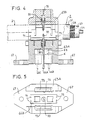
- the bypass socket 63 is composed of several parts which are specified in connection with FIGS. 4, 5 and 6, its base is here fixed in the half-shell 62A forming the bottom and on the printed circuit 65 lining said bottom.
- the positioning of the socket 63 is preferably chosen so that the portion of coaxial cable 2 which passes through said socket is in alignment with those by means of which this cable is fixed in the notches 67, by which it passes through the box 62.
- the isolation transformer 4 which connects the connection interface 1 to the coaxial cable is preferably housed in the bypass socket itself and the pins 66A, 66B, 66C, 66D for connection of the windings 4A and 4B of this transformer protrude directly under the socket base to allow direct connection to the printed circuit 65 ( Figure 2), for example provided with corresponding metallized holes for this purpose not referenced.
- the bypass socket is here composed of a hollow body, here in roughly square section, mounted on the base 67 by one end and provided with a lower cavity 68 for housing the transformer 4 and the passage of the connections leading to the pins 66 .
- the hollow body is transversely notched at its other end so as to form a transverse cable positioning cradle 69 in alignment with the notches in the cabinet.
- the bottom of the cradle 69 is for example semi-cylindrical, it is extended by parallel guide walls 74 for the cable; it comprises a central conductive needle 70 intended to penetrate the cable and come to bite at its end into the conductive core 2A of this cable.
- the conductive needle 70 is covered by an insulating sheath, in its projecting part in the cradle 69, with the exception of its extreme tip, it is connected to a first end of the first winding of the transformer 3, which here is also outlet out of the socket via the pin 66A.
- the bottom of the cradle 69 is provided with conductive tips 71 intended to bite into the external conductor 2B of the coaxial cable 2 through the external insulating sheath 2C of this cable.
- the conducting tips 71 are here equally distributed on either side of the needle central 70 in a rectangular arrangement whose width is less than the diameter of the outer conductor 2B; here they are electrically connected to the second end of the first winding 4A of the transformer 4, via a tongue which continues under the base by the pin 66B.
- the conductive tips 71 four in number come from the same piece extending after bending to form the pin 66B.
- the coaxial cable 2 is immobilized in the hollow body 63A by a plug 63B which is embedded in the transverse notch for the passage of the coaxial cable above said cable on which the plug is supported by a concave surface 72, of parallel axis to that of the cradle 69.
- the plug 63B is here fixed to the hollow body 63A by snap-fastening, under the action of a tool not shown, it has for this purpose lateral openings 73 allowing the passage of the ends of the guide walls 74 of the hollow body which are provided with this effect of notches 75 and having a relative elasticity.
- the plug 63B is also provided with a needle 76 intended to be positioned in the axis of the central needle 70 on the other side of the core of the coaxial cable 2 in which it also comes to bite.
- This needle 76 which is intended to promote the penetration of the central needle 70 to the core 2A of the coaxial cable during assembly of the socket, also participates in maintaining the permanence of the contacts between core 2A and needles despite the possible vibrations or aging, thanks to the thrust it applies to this core together with the central needle under the action of elastic elements 80, here cylindrical, which, respectively housed in the hollow body and in the plug, tend to push the needles towards the soul.
Landscapes
- Details Of Connecting Devices For Male And Female Coupling (AREA)
- Coupling Device And Connection With Printed Circuit (AREA)
- Cable Transmission Systems, Equalization Of Radio And Reduction Of Echo (AREA)
- Communication Cables (AREA)
- Testing Of Short-Circuits, Discontinuities, Leakage, Or Incorrect Line Connections (AREA)
- Dc Digital Transmission (AREA)
- Insulated Conductors (AREA)
Priority Applications (1)
| Application Number | Priority Date | Filing Date | Title |
|---|---|---|---|
| AT87401392T ATE78646T1 (de) | 1986-06-20 | 1987-06-19 | Schnittstelle zur verbindung eines geraets mit einem koaxialen kabel. |
Applications Claiming Priority (2)
| Application Number | Priority Date | Filing Date | Title |
|---|---|---|---|
| FR8608930 | 1986-06-20 | ||
| FR8608930A FR2600475B1 (fr) | 1986-06-20 | 1986-06-20 | Interface de liaison d'un appareillage a un cable coaxial et coupleur incorporant une telle interface |
Publications (3)
| Publication Number | Publication Date |
|---|---|
| EP0250334A2 true EP0250334A2 (de) | 1987-12-23 |
| EP0250334A3 EP0250334A3 (en) | 1988-08-10 |
| EP0250334B1 EP0250334B1 (de) | 1992-07-22 |
Family
ID=9336522
Family Applications (1)
| Application Number | Title | Priority Date | Filing Date |
|---|---|---|---|
| EP87401392A Expired - Lifetime EP0250334B1 (de) | 1986-06-20 | 1987-06-19 | Schnittstelle zur Verbindung eines Geräts mit einem koaxialen Kabel |
Country Status (7)
| Country | Link |
|---|---|
| EP (1) | EP0250334B1 (de) |
| AT (1) | ATE78646T1 (de) |
| BR (1) | BR8703090A (de) |
| DE (1) | DE3780520T2 (de) |
| ES (1) | ES2033897T3 (de) |
| FR (1) | FR2600475B1 (de) |
| GR (1) | GR3005832T3 (de) |
Cited By (1)
| Publication number | Priority date | Publication date | Assignee | Title |
|---|---|---|---|---|
| EP0421174A3 (en) * | 1989-09-30 | 1991-12-27 | Franz Leinbach | Connecting device for a local area network |
Family Cites Families (8)
| Publication number | Priority date | Publication date | Assignee | Title |
|---|---|---|---|---|
| US4266842A (en) * | 1979-09-17 | 1981-05-12 | Zerox Corporation | Transmission line active coaxial tap |
| GB2064918B (en) * | 1979-12-01 | 1983-12-21 | British Aerospace | Data communication systems |
| US4337465A (en) * | 1980-09-25 | 1982-06-29 | Burroughs Corporation | Line driver circuit for a local area contention network |
| EP0105337A1 (de) * | 1982-03-29 | 1984-04-18 | Ncr Corporation | Datenübertragungsnetz und übertragungsverfahren |
| US4588249A (en) * | 1982-11-03 | 1986-05-13 | Amp Incorporated | Coaxial cable tap connector |
| JPS59158644A (ja) * | 1983-02-28 | 1984-09-08 | Toshiba Corp | デ−タ伝送システム |
| FR2544569B1 (fr) * | 1983-04-13 | 1986-07-04 | Commissariat Energie Atomique | Dispositif de couplage par induction entre une ligne electrique de transmission d'informations et une station d'emission et/ou de reception d'informations |
| EP0145407B1 (de) * | 1983-11-28 | 1991-01-23 | Ing. C. Olivetti & C., S.p.A. | Vorrichtung zum Verbinden einer logischen Schaltung mit einem koaxialen Kabel |
-
1986
- 1986-06-20 FR FR8608930A patent/FR2600475B1/fr not_active Expired
-
1987
- 1987-06-19 BR BR8703090A patent/BR8703090A/pt not_active IP Right Cessation
- 1987-06-19 ES ES198787401392T patent/ES2033897T3/es not_active Expired - Lifetime
- 1987-06-19 DE DE8787401392T patent/DE3780520T2/de not_active Expired - Lifetime
- 1987-06-19 EP EP87401392A patent/EP0250334B1/de not_active Expired - Lifetime
- 1987-06-19 AT AT87401392T patent/ATE78646T1/de not_active IP Right Cessation
-
1992
- 1992-09-30 GR GR920402163T patent/GR3005832T3/el unknown
Cited By (1)
| Publication number | Priority date | Publication date | Assignee | Title |
|---|---|---|---|---|
| EP0421174A3 (en) * | 1989-09-30 | 1991-12-27 | Franz Leinbach | Connecting device for a local area network |
Also Published As
| Publication number | Publication date |
|---|---|
| ATE78646T1 (de) | 1992-08-15 |
| EP0250334B1 (de) | 1992-07-22 |
| EP0250334A3 (en) | 1988-08-10 |
| ES2033897T3 (es) | 1993-04-01 |
| FR2600475A1 (fr) | 1987-12-24 |
| DE3780520T2 (de) | 1992-12-17 |
| FR2600475B1 (fr) | 1988-08-26 |
| DE3780520D1 (de) | 1992-08-27 |
| BR8703090A (pt) | 1988-03-08 |
| GR3005832T3 (de) | 1993-06-07 |
Similar Documents
| Publication | Publication Date | Title |
|---|---|---|
| EP2011197B1 (de) | Hochbandbreitenverbinder | |
| FR2771554A1 (fr) | Connecteur electrique a fiche modulaire | |
| EP0056545A1 (de) | Einrichtung zur Fernortung von Unterbrechungen und Kurzschlüssen in einer Zweidrahtleitung | |
| WO2007085734A1 (fr) | Dispositif amovible d'injection de puissance electrique pour reseau ethernet | |
| FR2666695A1 (fr) | Connecteur pour cable de type paire blindee a drain de masse. | |
| FR2463568A1 (fr) | Connecteur de transition pour cables coaxiaux | |
| EP4270700B1 (de) | Verbindungsgehäuse für einpaar-ethernet-kabel und zugehörige verdrahtete ethernet-netzwerke | |
| EP0228741B1 (de) | Testvorrichtung für ein Gehäuse ohne Kontaktnadeln, versehen mit einem mit Hochfrequenz arbeitenden Chip mit integrierter Schaltung | |
| EP0250334A2 (de) | Schnittstelle zur Verbindung eines Geräts mit einem koaxialen Kabel | |
| EP2051396A1 (de) | Online-Übertragung durch Trägerstrom | |
| EP0063502A1 (de) | Anordnung zur Fehlerortung auf einer zweiadrigen Leitung | |
| EP0537444B1 (de) | Vorrichtung zum Verbinden eines Übertragungsnetzes mit einer Vielzahl von Teilnehmern | |
| FR2589288A1 (fr) | Dispositif de connexion decentralisee d'un organe a une unite de commande programmable | |
| FR2544569A1 (fr) | Dispositif de couplage par induction entre une ligne electrique de transmission d'informations et une station d'emission et/ou de reception d'informations | |
| FR2599917A1 (fr) | Circuit de commutation de reseaux d'equilibrage | |
| FR2800221A1 (fr) | Dispositif et boitier pour raccordement a un reseau local | |
| FR2696603A1 (fr) | Tête laser perfectionnée. | |
| EP0866405B1 (de) | Digitales Kommunikationsbus zur Verbindung von elektronischen Modulen | |
| EP0589786B1 (de) | Verbindervorrichtung für Signalübertragungseinrichtung | |
| FR2615669A1 (fr) | Dispositif de limitation des perturbations electriques a l'enfichage et au defichage d'une carte electronique | |
| EP0320356B1 (de) | Leistungsreihenklemme, die Steckerstifte trägt | |
| EP1582001B1 (de) | Informationsaustauschanordnung zwischen ein sendergerät und ein empfängergerät | |
| FR2696304A1 (fr) | Dispositif pour transférer des données dans des systèmes de contrôle de processus. | |
| EP1003292B1 (de) | Verfahren zur Extraktion von elektrischen Signalen ohne Unterbrechung des Leitungspaares | |
| EP4723396A1 (de) | Elektrischer steckverbinder für ein haus-gateway mit erkennung des einsetzens eines elektrischen steckverbinders |
Legal Events
| Date | Code | Title | Description |
|---|---|---|---|
| PUAI | Public reference made under article 153(3) epc to a published international application that has entered the european phase |
Free format text: ORIGINAL CODE: 0009012 |
|
| AK | Designated contracting states |
Kind code of ref document: A2 Designated state(s): AT BE CH DE ES FR GB GR IT LI LU NL SE |
|
| PUAL | Search report despatched |
Free format text: ORIGINAL CODE: 0009013 |
|
| AK | Designated contracting states |
Kind code of ref document: A3 Designated state(s): AT BE CH DE ES FR GB GR IT LI LU NL SE |
|
| 17P | Request for examination filed |
Effective date: 19880914 |
|
| RAP1 | Party data changed (applicant data changed or rights of an application transferred) |
Owner name: SOCIETE ANONYME DITE: CEGELEC |
|
| 17Q | First examination report despatched |
Effective date: 19910311 |
|
| GRAA | (expected) grant |
Free format text: ORIGINAL CODE: 0009210 |
|
| ITTA | It: last paid annual fee | ||
| AK | Designated contracting states |
Kind code of ref document: B1 Designated state(s): AT BE CH DE ES FR GB GR IT LI LU NL SE |
|
| REF | Corresponds to: |
Ref document number: 78646 Country of ref document: AT Date of ref document: 19920815 Kind code of ref document: T |
|
| REF | Corresponds to: |
Ref document number: 3780520 Country of ref document: DE Date of ref document: 19920827 |
|
| GBT | Gb: translation of ep patent filed (gb section 77(6)(a)/1977) | ||
| ITF | It: translation for a ep patent filed | ||
| REG | Reference to a national code |
Ref country code: GR Ref legal event code: FG4A Free format text: 3005832 |
|
| REG | Reference to a national code |
Ref country code: ES Ref legal event code: FG2A Ref document number: 2033897 Country of ref document: ES Kind code of ref document: T3 |
|
| PGFP | Annual fee paid to national office [announced via postgrant information from national office to epo] |
Ref country code: GB Payment date: 19930422 Year of fee payment: 7 |
|
| PGFP | Annual fee paid to national office [announced via postgrant information from national office to epo] |
Ref country code: ES Payment date: 19930518 Year of fee payment: 7 |
|
| PGFP | Annual fee paid to national office [announced via postgrant information from national office to epo] |
Ref country code: DE Payment date: 19930519 Year of fee payment: 7 Ref country code: CH Payment date: 19930519 Year of fee payment: 7 |
|
| PGFP | Annual fee paid to national office [announced via postgrant information from national office to epo] |
Ref country code: SE Payment date: 19930521 Year of fee payment: 7 |
|
| PGFP | Annual fee paid to national office [announced via postgrant information from national office to epo] |
Ref country code: FR Payment date: 19930527 Year of fee payment: 7 |
|
| PLBE | No opposition filed within time limit |
Free format text: ORIGINAL CODE: 0009261 |
|
| STAA | Information on the status of an ep patent application or granted ep patent |
Free format text: STATUS: NO OPPOSITION FILED WITHIN TIME LIMIT |
|
| PGFP | Annual fee paid to national office [announced via postgrant information from national office to epo] |
Ref country code: GR Payment date: 19930528 Year of fee payment: 7 |
|
| PGFP | Annual fee paid to national office [announced via postgrant information from national office to epo] |
Ref country code: BE Payment date: 19930616 Year of fee payment: 7 |
|
| PGFP | Annual fee paid to national office [announced via postgrant information from national office to epo] |
Ref country code: NL Payment date: 19930630 Year of fee payment: 7 Ref country code: AT Payment date: 19930630 Year of fee payment: 7 |
|
| PGFP | Annual fee paid to national office [announced via postgrant information from national office to epo] |
Ref country code: LU Payment date: 19930701 Year of fee payment: 7 |
|
| 26N | No opposition filed | ||
| EPTA | Lu: last paid annual fee | ||
| PG25 | Lapsed in a contracting state [announced via postgrant information from national office to epo] |
Ref country code: LU Free format text: LAPSE BECAUSE OF NON-PAYMENT OF DUE FEES Effective date: 19940619 Ref country code: GB Effective date: 19940619 Ref country code: AT Effective date: 19940619 |
|
| PG25 | Lapsed in a contracting state [announced via postgrant information from national office to epo] |
Ref country code: SE Effective date: 19940620 Ref country code: ES Free format text: LAPSE BECAUSE OF THE APPLICANT RENOUNCES Effective date: 19940620 |
|
| PG25 | Lapsed in a contracting state [announced via postgrant information from national office to epo] |
Ref country code: LI Effective date: 19940630 Ref country code: CH Effective date: 19940630 Ref country code: BE Effective date: 19940630 |
|
| BERE | Be: lapsed |
Owner name: CEGELEC Effective date: 19940630 |
|
| PG25 | Lapsed in a contracting state [announced via postgrant information from national office to epo] |
Ref country code: GR Free format text: THE PATENT HAS BEEN ANNULLED BY A DECISION OF A NATIONAL AUTHORITY Effective date: 19941231 |
|
| PG25 | Lapsed in a contracting state [announced via postgrant information from national office to epo] |
Ref country code: NL Effective date: 19950101 |
|
| EUG | Se: european patent has lapsed |
Ref document number: 87401392.3 Effective date: 19950110 |
|
| GBPC | Gb: european patent ceased through non-payment of renewal fee |
Effective date: 19940619 |
|
| NLV4 | Nl: lapsed or anulled due to non-payment of the annual fee | ||
| PG25 | Lapsed in a contracting state [announced via postgrant information from national office to epo] |
Ref country code: FR Effective date: 19950228 |
|
| REG | Reference to a national code |
Ref country code: CH Ref legal event code: PL |
|
| PG25 | Lapsed in a contracting state [announced via postgrant information from national office to epo] |
Ref country code: DE Effective date: 19950301 |
|
| EUG | Se: european patent has lapsed |
Ref document number: 87401392.3 |
|
| REG | Reference to a national code |
Ref country code: FR Ref legal event code: ST Ref country code: GR Ref legal event code: MM2A Free format text: 3005832 |
|
| REG | Reference to a national code |
Ref country code: ES Ref legal event code: FD2A Effective date: 19991007 |
|
| PG25 | Lapsed in a contracting state [announced via postgrant information from national office to epo] |
Ref country code: IT Free format text: LAPSE BECAUSE OF NON-PAYMENT OF DUE FEES;WARNING: LAPSES OF ITALIAN PATENTS WITH EFFECTIVE DATE BEFORE 2007 MAY HAVE OCCURRED AT ANY TIME BEFORE 2007. THE CORRECT EFFECTIVE DATE MAY BE DIFFERENT FROM THE ONE RECORDED. Effective date: 20050619 |