EP0250620B1 - Procédé et dispositif pour tester électriquement des circuits imprimés - Google Patents
Procédé et dispositif pour tester électriquement des circuits imprimés Download PDFInfo
- Publication number
- EP0250620B1 EP0250620B1 EP86108680A EP86108680A EP0250620B1 EP 0250620 B1 EP0250620 B1 EP 0250620B1 EP 86108680 A EP86108680 A EP 86108680A EP 86108680 A EP86108680 A EP 86108680A EP 0250620 B1 EP0250620 B1 EP 0250620B1
- Authority
- EP
- European Patent Office
- Prior art keywords
- contact
- conductor
- connection
- potential
- circuit board
- Prior art date
- Legal status (The legal status is an assumption and is not a legal conclusion. Google has not performed a legal analysis and makes no representation as to the accuracy of the status listed.)
- Expired - Lifetime
Links
- 238000012360 testing method Methods 0.000 title claims abstract description 106
- 238000000034 method Methods 0.000 title claims description 36
- 239000004020 conductor Substances 0.000 claims abstract description 93
- 238000009413 insulation Methods 0.000 claims abstract description 15
- 239000000919 ceramic Substances 0.000 claims abstract description 3
- 238000010998 test method Methods 0.000 claims abstract description 3
- 238000003780 insertion Methods 0.000 claims description 2
- 230000037431 insertion Effects 0.000 claims description 2
- 238000005259 measurement Methods 0.000 description 16
- 238000011161 development Methods 0.000 description 9
- 230000018109 developmental process Effects 0.000 description 9
- 238000012937 correction Methods 0.000 description 4
- 238000006073 displacement reaction Methods 0.000 description 4
- 239000010408 film Substances 0.000 description 3
- 230000006978 adaptation Effects 0.000 description 2
- 238000010276 construction Methods 0.000 description 2
- 230000005669 field effect Effects 0.000 description 2
- 229910000831 Steel Inorganic materials 0.000 description 1
- 239000000969 carrier Substances 0.000 description 1
- 238000013461 design Methods 0.000 description 1
- 238000004519 manufacturing process Methods 0.000 description 1
- 230000035945 sensitivity Effects 0.000 description 1
- 239000010959 steel Substances 0.000 description 1
- 239000010409 thin film Substances 0.000 description 1
- 230000007704 transition Effects 0.000 description 1
- 238000011144 upstream manufacturing Methods 0.000 description 1
Images

Classifications
-
- G—PHYSICS
- G01—MEASURING; TESTING
- G01R—MEASURING ELECTRIC VARIABLES; MEASURING MAGNETIC VARIABLES
- G01R1/00—Details of instruments or arrangements of the types included in groups G01R5/00 - G01R13/00 and G01R31/00
- G01R1/02—General constructional details
- G01R1/06—Measuring leads; Measuring probes
- G01R1/067—Measuring probes
- G01R1/073—Multiple probes
-
- G—PHYSICS
- G01—MEASURING; TESTING
- G01R—MEASURING ELECTRIC VARIABLES; MEASURING MAGNETIC VARIABLES
- G01R31/00—Arrangements for testing electric properties; Arrangements for locating electric faults; Arrangements for electrical testing characterised by what is being tested not provided for elsewhere
- G01R31/28—Testing of electronic circuits, e.g. by signal tracer
- G01R31/2801—Testing of printed circuits, backplanes, motherboards, hybrid circuits or carriers for multichip packages [MCP]
- G01R31/281—Specific types of tests or tests for a specific type of fault, e.g. thermal mapping, shorts testing
Definitions
- connection points While typically half to two thirds of the total connection points in printed circuit boards are distributed over a large number of printed conductors of a relatively short length, the rest of the connection points are distributed over the voltage supply and the clock supply conductor strips. Since such conductor tracks are naturally very long and therefore have many connection points, there are considerable problems as a result of the leakage currents of the transistors connected to these connection points when measuring the insulation between these conductor tracks and other conductor tracks. In reality, for example, approximately 30% of the total connection points of a printed circuit board are located on the conductor track carrying "Ground", while approximately 15% of the connection points are located on the conductor track carrying the supply voltage Vcc. One of the reasons for this is that the inputs of a large number of components are grounded when they are not being used.
- the object of the present invention is therefore to provide a method for the electrical testing of printed circuit boards, by means of which an accurate measurement of the insulation resistance between a relatively long printed conductor and other printed conductors of a printed circuit board is made possible.
- the present invention is intended to provide devices for carrying out this method.
- a major advantage of the method according to the invention is that the insulation resistance between relatively long conductor tracks and other conductor tracks of a printed circuit board can be measured in a relatively simple and uncomplicated manner by executing only a simple additional step after measuring the conductivity of the conductor tracks.
- the insulation measurements can advantageously be carried out with the greatest possible sensitivity.
- the devices for carrying out the method according to the invention are advantageously of simple construction and easy to handle.
- a further development of the method according to the invention is particularly advantageous, according to which a mask is introduced between the ends of the test pins of the adapter device facing the printed circuit board and the printed circuit board and is aligned in such a way that one test pin per conductor track protrudes through an opening in the mask in order to establish an electrical connection between the to establish a respective connection point of the conductor track and the first and second electronic switches.
- the manufacture of such a mask is advantageously relatively simple.
- the mask has the shape of a thin insulating plate with openings. With a possible spring travel of the contact elements of the grid of 2 to 6 mm, such a plate preferably has a thickness of approximately 0.2 mm.
- the mask is particularly easy to use if adjustment devices are provided, by means of which the mask can be brought into a position aligned with the conductor track before the other method steps are carried out.
- the circuit board is then raised while maintaining its aligned position in such a way that the electrical connections between the short test pins and the connection points of the conductor tracks assigned to them are interrupted, and that an electrical connection between the respective one is made via a long test pin per conductor track Connection point of the conductor track and the corresponding contact element of the contact field remains.
- the adapter for carrying out this development of the present method has short and longer test pins, with a longer test pin being arranged in such a way that it is assigned to a specific connection point of a conductor track of the printed circuit board and the length difference between the short and long test pins is smaller than that possible travel of the contact elements of the grid assigned to the adapter.
- An adaptation device is particularly preferred in which the length difference between the short and longer test pins with a possible spring travel of the contact elements of approximately 4 to 8 mm is in a range of approximately 2 to 3 mm.
- a displacement device is preferably provided to simplify an exact displacement of the printed circuit board, which ensures that the printed circuit board can be moved a predetermined distance in the longitudinal direction of the test pins while maintaining its position aligned with the test pins.
- the grid-bound intermediate contact field preferably has through holes at the individual grid points on, selectively rigid contact members can be used to make the electrical connections.
- the intermediate contact field consists of an insulating plate, in the through holes of which pin-like elements can be selectively used as contact members.
- pin-like contact members are particularly easy to handle if they have projections which extend beyond their circumference and which serve as stops and end the insertion movement from one side of the intermediate contact field.
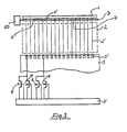
- a circuit board to be tested is designated by 1.
- This circuit board 1 has plated-through holes or connection points 1 ', which are brought into contact in a manner known per se with the tips of test pins 2, an adapter 2 facing them, that the circuit board 1, after it has been brought into the correct position, is pressed against the tips of the test pins 2 '.
- a grid 3 is arranged, which has, for example, resilient contact elements 3 'into which the tips or ends of the test pins 2' remote from the printed circuit board 1 engage.
- Each contact element 3 ' is connected to an electronic switch 4, 8.
- Transistors preferably MOS field-effect transistors, are provided as electronic switches 4, 8, for example, which are selectively controlled by a control device 5 for carrying out the individual test steps.
- each connection point 1 'of the circuit board 1 is connected to ground via a transistor 4 and to a measuring voltage Vcc via a transistor 8 with the interposition of a current measuring device 6.
- transistors 4, 8 are shown as switches in FIG. 2.
- the networks A, B, F and G each comprise a connection point 1 '.
- the network C comprises six connection points 1' along its length Trace 1 ".
- the network D comprises four connection points 1 'along its conductor track 1 ".
- the network E has two connection points 1' on its conductor track 1 " .
- connection point 1 'to connection point 1' When testing for the conductivity of a specific conductor track 1 ", the procedure is such that the test is carried out from connection point 1 'to connection point 1'.
- the transistors 4, 8 are controlled by the control device 5 such that only two in one test step Transistors are connected in such a way that there is a connection between ground and a connection point 1 'via a transistor and a connection between the measuring voltage Vcc and another connection point 1' via the other transistor All other transistors 4, 8 which are assigned to the specific conductor track are blocked in this test step by the control device 5.
- the transistors C' and C are closed, so that a current flow between ground, the transistor C", the intact Area of trace 1 "of network C between the left two Connection points 1 ', the transistor C', the measuring device 6 and the potential Vcc.
- the network C is to be tested with regard to its insulation resistance
- a further test step only a single connection point of the network C is connected to the measuring potential Vcc via a transistor and the measuring device 6. All other transistors 4, 8, which are connected to the end points 1 'of the network C, are opened. 2, only the left connection point 1 'of the network C is connected to the measuring device 6 or the measurement potential Vcc via the closed transistor C ' . It can be seen that during this measuring step the leakage currents of all transistors 4, which are connected to the connection points 1 'of the network C, add up. If the number of connection points 1 'of the network C is very large, the above-mentioned falsifications of the measurement result occur.
- connection point 1 'used for the measurement in the second test step per conductor track 1' is referred to as the primary point.
- connection points 1 ′ of the conductor tracks 1 ′′ which are not primary points, can be masked out, which are introduced between the circuit board 1 and the adapter device 2 in this way during the execution of the second test step according to FIG 3, such a mask is designated by 7.
- this mask 7, which is individually made for special circuit board patterns, has openings 7, which after the mask 7 has been aligned with respect to the special printed circuit board 1 so that only certain test pins 2 'can pass through them and make contact with the primary points.
- Mask 7 prevents an electrical connection between all other connection points 1' and the test pins 2 ' Contact is made because the mask 7 assigned to these connection points neten areas has no openings through which the corresponding test pins 2 'could pass.
- the thickness of the mask 7, which preferably has the shape of a thin plate, with a possible spring travel of the contact elements 3 'of the grid 3 of 2-6 mm, preferably about 0.2 mm.
- the adapting device preferably has adjustment devices 50 which ensure that the mask 7 can be quickly brought into the position aligned with the printed circuit board 1 before the second test steps for measuring the insulation resistances are carried out.
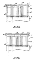
- FIGS. 4a and 4b A particularly preferred embodiment of the invention can be seen from FIGS. 4a and 4b.
- an adapter device 20 is used in which there are different test pins 20 ' and 20 ", each of which is resilient in its longitudinal direction.
- the test pins 20 have ' a shorter spring travel than the test pins 20 " . It is thereby achieved that the circuit board 1 can be pressed against the adapter device 20 in such a way that all tips of the test pins 20 'and 20 "facing it are in contact with corresponding connection points 1' of the circuit board 1 for carrying out the first test steps (FIG. 4a), because the test pins 20 ′′ are pushed together or shortened until the tips of the test pins 20 ′ rest on the corresponding connection points 1 ′ of the printed circuit board 1.
- the circuit board 1 is raised so far while maintaining its position in relation to the adapter device 20 that only test pins 20 "assigned to the primary points, which have the longer spring travel, are in contact with the primary points assigned to them.
- This embodiment is advantageous compared to the embodiment shown in Figure 3 because it is not necessary to insert and adjust a mask 7. In the transition from the first to the second test steps, it is only necessary to hold the circuit board 1 in its current position and one In this way, time can be saved in comparison with the embodiment shown in FIG.
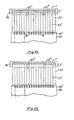
- the contact elements which are assigned to the primary points are then pressed in further by the longer test pins 21 " than the other test pins 21 '.
- the printed circuit board 1 is then lifted upwards until measurement is complete until only the test pins 21 ′′ assigned to the primary points establish electrical connections between the grid contact field 30 and the printed circuit boards 1 on account of their greater lengths.
- the length difference between the test pins 21 'and 21 " is preferably approximately 2-3 mm with a possible spring travel of the contact elements 30' of the grid field 30 of approximately 4-8 mm.
- displacement devices are preferably provided, by means of which an automatic displacement of the printed circuit board 1 in the longitudinal direction of the test pins is possible while maintaining their position aligned with the test pins between the first and second test steps.
- Such shifting devices are shown schematically in the figures mentioned and designated 40.
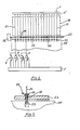
- FIGS. 6 and 7 show a further device for carrying out the method according to the invention, which has an intermediate contact field 53 which is inserted between the ends of the test pins 51 of an adapter device 57 facing the contact field 55 and the contact field 55 before the other method steps are carried out.
- the intermediate contact pad 53 is preferably in the form of an electrically insulating plate which is provided with through holes 58 which correspond to the grid of the con Clock field 55 are provided.
- the intermediate contact field 53 is aligned with the aid of a stop element 56 shown schematically in FIG. 6 in relation to the contact field 55 in such a way that the through holes 58 are aligned with the contact elements 52 of the contact field 55.
- Contact members 54 can be selectively introduced into individual through holes 58, which establish electrical connections between individual test pins 51 and the corresponding contact elements 52 of the contact field 55.
- the contact members 54 are selectively arranged according to the primary points.
- FIG. 7 which schematically shows a contact member 54 inserted into a through hole 58 of an insulating plate forming the intermediate contact field 53, shows that this contact member 54 preferably has the shape of a pin-like element which is provided with a shoulder 59 on one side which, when the pin-like contact member 54 is selectively inserted, prevents the pin-like contact member 54 from passing through the corresponding through hole 58.
- electrical connections between the primary points of the printed circuit board 1 are only established via the selectively provided contact elements 54, which bring about electrical connections between the test pins 51 assigned to them and the corresponding contact elements 52.
- a major advantage of this adapter device is that the selective fitting of the intermediate contact pad 53 in the form of an electrically insulating plate with the contact members 54 is relatively simple because the locations at which these contact members 54 are to be selectively arranged can be specified very easily in coordinates , so that 13 an automatic assembly of the intermediate contact field 53 can take place.
- This automatic assembly can be carried out particularly simply, for example, in such a way that an additional thin film, which can expediently be made of plastic or paper, is used, which has openings 53 only at the through holes 58 to be populated in the grid-bound intermediate contact field.
- This film is first aligned with the intermediate contact field 53 and placed or applied thereon.
- a grid-bound cassette or the like which has a contact element 54 at each grid point, is aligned with the intermediate contact field 53 and handled and placed on the intermediate contact field 53 in such a way that only the contact elements 54 fall out of it and enter corresponding through holes 58 of the intermediate contact field 53, which are provided at the locations where an opening of the film is aligned with a through hole 58. All other contact members 54 of the cassette cannot enter the intermediate contact field 53 or corresponding through holes 58 of the same, because the film has no openings at the locations of these through holes 58.
Landscapes
- Engineering & Computer Science (AREA)
- Physics & Mathematics (AREA)
- General Physics & Mathematics (AREA)
- Computer Hardware Design (AREA)
- Microelectronics & Electronic Packaging (AREA)
- General Engineering & Computer Science (AREA)
- Testing Of Short-Circuits, Discontinuities, Leakage, Or Incorrect Line Connections (AREA)
- Tests Of Electronic Circuits (AREA)
Claims (16)
Priority Applications (6)
| Application Number | Priority Date | Filing Date | Title |
|---|---|---|---|
| AT86108680T ATE56280T1 (de) | 1986-06-25 | 1986-06-25 | Verfahren und vorrichtung zum elektrischen pruefen von leiterplatten. |
| EP86108680A EP0250620B1 (fr) | 1986-06-25 | 1986-06-25 | Procédé et dispositif pour tester électriquement des circuits imprimés |
| DE8686108680T DE3674000D1 (de) | 1986-06-25 | 1986-06-25 | Verfahren und vorrichtung zum elektrischen pruefen von leiterplatten. |
| JP61216081A JPS635274A (ja) | 1986-06-25 | 1986-09-16 | プリント基板を検査するための方法と装置 |
| CA000540314A CA1287184C (fr) | 1986-06-25 | 1987-06-23 | Essai de cartes a circuit imprime par recours a l'isolation mecanique |
| US07/469,717 US4952871A (en) | 1986-06-25 | 1990-01-24 | Method and apparatus of testing printed circuit boards and assembly employable therewith |
Applications Claiming Priority (1)
| Application Number | Priority Date | Filing Date | Title |
|---|---|---|---|
| EP86108680A EP0250620B1 (fr) | 1986-06-25 | 1986-06-25 | Procédé et dispositif pour tester électriquement des circuits imprimés |
Publications (2)
| Publication Number | Publication Date |
|---|---|
| EP0250620A1 EP0250620A1 (fr) | 1988-01-07 |
| EP0250620B1 true EP0250620B1 (fr) | 1990-09-05 |
Family
ID=8195222
Family Applications (1)
| Application Number | Title | Priority Date | Filing Date |
|---|---|---|---|
| EP86108680A Expired - Lifetime EP0250620B1 (fr) | 1986-06-25 | 1986-06-25 | Procédé et dispositif pour tester électriquement des circuits imprimés |
Country Status (6)
| Country | Link |
|---|---|
| US (1) | US4952871A (fr) |
| EP (1) | EP0250620B1 (fr) |
| JP (1) | JPS635274A (fr) |
| AT (1) | ATE56280T1 (fr) |
| CA (1) | CA1287184C (fr) |
| DE (1) | DE3674000D1 (fr) |
Families Citing this family (19)
| Publication number | Priority date | Publication date | Assignee | Title |
|---|---|---|---|---|
| US5157325A (en) * | 1991-02-15 | 1992-10-20 | Compaq Computer Corporation | Compact, wireless apparatus for electrically testing printed circuit boards |
| EP0508561B1 (fr) | 1991-04-11 | 1996-07-17 | METHODE ELECTRONICS, Inc. | Appareil pour tester électroniquement des plaques de circuits imprimés ou analogues |
| GB2265224B (en) * | 1992-03-20 | 1996-04-10 | Centalic Tech Dev Ltd | Testing apparatus |
| GB2278965B (en) * | 1993-06-07 | 1997-08-27 | Centalic Tech Dev Ltd | Testing Apparatus |
| US5485095A (en) * | 1994-11-10 | 1996-01-16 | International Business Machines Corporation | Fabrication test circuit and method for signalling out-of-spec resistance in integrated circuit structure |
| US6054720A (en) | 1997-11-06 | 2000-04-25 | International Business Machines Corporation | Apparatus and method for evaluating the surface insulation resistance of electronic assembly manufacture |
| JP3242883B2 (ja) * | 1998-08-05 | 2001-12-25 | 日東電工株式会社 | フレキシブル配線板の検査方法 |
| JP2000241485A (ja) * | 1999-02-24 | 2000-09-08 | Jsr Corp | 回路基板の電気抵抗測定装置および方法 |
| US6504378B1 (en) * | 1999-11-24 | 2003-01-07 | Micron Technology, Inc. | Apparatus for evaluating contact pin integrity of electronic components having multiple contact pins |
| US6424140B1 (en) * | 2000-05-03 | 2002-07-23 | Advanced Micro Devices, Inc. | Chip scale electrical test fixture |
| US6978214B2 (en) * | 2003-11-25 | 2005-12-20 | International Business Machines Corporation | Validation of electrical performance of an electronic package prior to fabrication |
| DE102006022686B4 (de) * | 2006-05-16 | 2018-03-15 | Sma Solar Technology Ag | Messanordnung zur Ermittlung des Isolationswiderstandes einer elektrischen Vorrichtung oder einer Anlage |
| CN101788612B (zh) * | 2009-01-23 | 2012-09-05 | 南亚电路板股份有限公司 | 印刷电路板的阻值测量模块及其测量方法 |
| CN102914670B (zh) * | 2012-10-24 | 2015-07-29 | 华东光电集成器件研究所 | 绝缘电阻测试夹具 |
| CN109471011A (zh) * | 2017-09-07 | 2019-03-15 | 新加坡商美亚国际电子有限公司 | 测试用电路板及其操作方法 |
| CN110058148B (zh) * | 2019-05-29 | 2021-06-15 | 深圳市凯码时代科技有限公司 | 转接电路板、转接夹具架构以及相应的电路转接方法 |
| CN110926815B (zh) * | 2019-12-05 | 2021-05-04 | 中国航发四川燃气涡轮研究院 | 一种航空发动机电气系统线路自动检测装置 |
| CN114594372B (zh) * | 2022-05-10 | 2022-08-12 | 东莞市新一电子有限公司 | 一种测试工装 |
| CN119716649B (zh) * | 2025-03-03 | 2025-05-27 | 成都光创联科技有限公司 | 一种光器件测试电路、测试方法 |
Family Cites Families (17)
| Publication number | Priority date | Publication date | Assignee | Title |
|---|---|---|---|---|
| DE2013070A1 (de) * | 1970-03-19 | 1971-09-30 | Licentia Gmbh | Verfahren und Vorrichtung zur Prüfung von unbestuckten gedruckten Schaltungs platten |
| BE806098A (fr) * | 1973-03-28 | 1974-02-01 | Siemens Ag | Procede de fabrication de silicium ou autre matiere semi-conductrice tres pure |
| DE2707900C3 (de) * | 1977-02-24 | 1980-09-04 | Ante 6980 Wertheim Milkovic | Universal-Adaptiervorrichtung für Geräte zur elektrischen Prüfung unterschiedlicher gedruckter Schaltungen |
| DE2915742C2 (de) * | 1979-04-19 | 1984-04-26 | Werner 7750 Konstanz Heilmann | Prüfvorrichtung für eine elektronische Schaltung |
| US4321533A (en) * | 1979-04-19 | 1982-03-23 | Fairchild Camera & Instrument Corp. | Printed circuit board test fixture having interchangeable card personalizers |
| DE2920226C2 (de) * | 1979-05-18 | 1983-04-07 | Siemens AG, 1000 Berlin und 8000 München | Adapter zum Anschluß von eine Vielzahl von rasterartig verteilten Anschlußpunkten aufweisenden Prüflingen |
| US4352061A (en) * | 1979-05-24 | 1982-09-28 | Fairchild Camera & Instrument Corp. | Universal test fixture employing interchangeable wired personalizers |
| US4496903A (en) * | 1981-05-11 | 1985-01-29 | Burroughs Corporation | Circuit board test fixture |
| US4471298A (en) * | 1981-12-11 | 1984-09-11 | Cirdyne, Inc. | Apparatus for automatically electrically testing printed circuit boards |
| DE3312436A1 (de) * | 1982-10-29 | 1984-05-03 | Feinmetall Gmbh, 7033 Herrenberg | Kontaktiervorrichtung |
| EP0115135A1 (fr) * | 1982-12-27 | 1984-08-08 | Genrad, Inc. | Fixation électrique pour tester des circuits imprimés et similaires |
| JPS6042662A (ja) * | 1983-08-17 | 1985-03-06 | Ibiden Co Ltd | プリント配線板の検査方法とその検査装置 |
| JPS60169777A (ja) * | 1984-02-13 | 1985-09-03 | Sharp Corp | 電気回路の接続装置 |
| US4626776A (en) * | 1984-06-07 | 1986-12-02 | O. B. Test Group, Inc. | Programmable test fixture |
| DE3524229A1 (de) * | 1984-07-10 | 1986-01-16 | Ingun Prüfmittelbau GmbH & Co KG Elektronik, 7750 Konstanz | Vorrichtung zum pruefen von pruefpunkten einer elektronischen leiterplatte od. dgl. als pruefling mittels kontaktstiften |
| US4626779A (en) * | 1985-03-19 | 1986-12-02 | Pylon Company, Inc. | Spring-stops for a bi-level test fixture |
| JPH02968A (ja) * | 1988-06-08 | 1990-01-05 | Fujitsu Ltd | フォトマスク |
-
1986
- 1986-06-25 DE DE8686108680T patent/DE3674000D1/de not_active Expired - Lifetime
- 1986-06-25 EP EP86108680A patent/EP0250620B1/fr not_active Expired - Lifetime
- 1986-06-25 AT AT86108680T patent/ATE56280T1/de not_active IP Right Cessation
- 1986-09-16 JP JP61216081A patent/JPS635274A/ja active Pending
-
1987
- 1987-06-23 CA CA000540314A patent/CA1287184C/fr not_active Expired - Lifetime
-
1990
- 1990-01-24 US US07/469,717 patent/US4952871A/en not_active Expired - Lifetime
Also Published As
| Publication number | Publication date |
|---|---|
| JPS635274A (ja) | 1988-01-11 |
| EP0250620A1 (fr) | 1988-01-07 |
| US4952871A (en) | 1990-08-28 |
| DE3674000D1 (de) | 1990-10-11 |
| ATE56280T1 (de) | 1990-09-15 |
| CA1287184C (fr) | 1991-07-30 |
Similar Documents
| Publication | Publication Date | Title |
|---|---|---|
| EP0250620B1 (fr) | Procédé et dispositif pour tester électriquement des circuits imprimés | |
| EP0285799B1 (fr) | Dispositif de test électrique du fonctionnement de rangées de fils électriques, en particulier pour cartes de circuit | |
| DE3408704C2 (de) | Verfahren zum Prüfen von starren oder flexiblen elektrischen Verbindungsnetzwerk-Schaltungen und Vorrichtung zur Durchführung des Verfahrens | |
| DE2744299C2 (de) | Verfahren zum elektrischen Prüfen eines Leiterbahnmusters auf einem Substrat | |
| DE2360801A1 (de) | Pruefeinrichtung mit kontaktiereinrichtung | |
| DE2525166A1 (de) | Kontakt-sondenvorrichtung | |
| DE3716240A1 (de) | Pruefadapter, insbesondere fuer eine integrierte schaltung | |
| DE2659977B1 (de) | Vorrichtung zur Herstellung einer elektrischen Verbindung zwischen einem in einer statischen elektrischen Pruefung befindlichen Bauteil und einer Pruefeinrichtung | |
| EP0838688B1 (fr) | Appareil et procédé de test de circuits imprimés | |
| EP0078339A1 (fr) | Dispositif de test pour pistes de circuit imprimé ayant au moins une tête comportant une multitude de contacts flexibles | |
| DE3318716A1 (de) | Anordnung fuer die zeitlagenbegradigung von hinsichtlich ihrer zeitlage kritischen signalen in automatischen pruefeinrichtungen | |
| DE10212617A1 (de) | Kallibrierung von Anschlüssen von Testgeräten für integrierte Schaltungen | |
| DE10109385A1 (de) | Kalibrierungsverfahren und -vorrichtung für Fassungen | |
| DE10260238B4 (de) | Adapter zum Testen einer oder mehrerer Leiteranordnungen und Verfahren | |
| DE2655841C3 (de) | Integrierter Widerstandsbaustein zum Einlöten in eine Flachbaugruppe | |
| DE19714941A1 (de) | Meßkarte und Ein/Ausgang-Anschlußtestsystem unter Verwendung derselben | |
| EP0322607A2 (fr) | Appareil de commande pour un dispositif pour le test de platines de circuits | |
| EP0489052B1 (fr) | Dispositif pour le controle du fonctionnement electrique de champs de cablage, en particulier de cartes de circuits imprimes | |
| DE3924763C2 (de) | Prüfeinrichtung für mehradrige elektrische Kabel | |
| DE2017151A1 (de) | Testadapter für Schaltungskarten | |
| WO1989008265A1 (fr) | Dispositif pour le controle de plaquettes de circuits imprimes | |
| DE2633175A1 (de) | Verfahren zur durchfuehrung von arbeitsschritten an mehreren schaltkreistraegern und vorrichtung zur durchfuehrung dieses verfahrens | |
| EP0286814A2 (fr) | Dispositif de commande | |
| DE4309842C1 (de) | Verfahren zum Testen von Platinen und Vorrichtung zur Durchführung des Verfahrens | |
| DE10320622A1 (de) | Verfahren und Vorrichtung zum Bestimmen korrekter Spurbreiten für eine gedruckte Schaltungsplatine einer drahtlosen Testhalterung |
Legal Events
| Date | Code | Title | Description |
|---|---|---|---|
| PUAI | Public reference made under article 153(3) epc to a published international application that has entered the european phase |
Free format text: ORIGINAL CODE: 0009012 |
|
| 17P | Request for examination filed |
Effective date: 19870630 |
|
| AK | Designated contracting states |
Kind code of ref document: A1 Designated state(s): AT BE CH DE FR GB IT LI LU NL SE |
|
| RAP1 | Party data changed (applicant data changed or rights of an application transferred) |
Owner name: MANIA ELEKTRONIK AUTOMATISATION ENTWICKLUNG UND GE |
|
| 17Q | First examination report despatched |
Effective date: 19880408 |
|
| GRAA | (expected) grant |
Free format text: ORIGINAL CODE: 0009210 |
|
| AK | Designated contracting states |
Kind code of ref document: B1 Designated state(s): AT BE CH DE FR GB IT LI LU NL SE |
|
| ITF | It: translation for a ep patent filed | ||
| PG25 | Lapsed in a contracting state [announced via postgrant information from national office to epo] |
Ref country code: SE Effective date: 19900905 |
|
| REF | Corresponds to: |
Ref document number: 56280 Country of ref document: AT Date of ref document: 19900915 Kind code of ref document: T |
|
| GBT | Gb: translation of ep patent filed (gb section 77(6)(a)/1977) | ||
| REF | Corresponds to: |
Ref document number: 3674000 Country of ref document: DE Date of ref document: 19901011 |
|
| ET | Fr: translation filed | ||
| PGFP | Annual fee paid to national office [announced via postgrant information from national office to epo] |
Ref country code: LU Payment date: 19910621 Year of fee payment: 6 |
|
| PG25 | Lapsed in a contracting state [announced via postgrant information from national office to epo] |
Ref country code: AT Effective date: 19910625 |
|
| ITTA | It: last paid annual fee | ||
| PLBE | No opposition filed within time limit |
Free format text: ORIGINAL CODE: 0009261 |
|
| STAA | Information on the status of an ep patent application or granted ep patent |
Free format text: STATUS: NO OPPOSITION FILED WITHIN TIME LIMIT |
|
| 26N | No opposition filed | ||
| EPTA | Lu: last paid annual fee | ||
| PG25 | Lapsed in a contracting state [announced via postgrant information from national office to epo] |
Ref country code: LU Free format text: LAPSE BECAUSE OF NON-PAYMENT OF DUE FEES Effective date: 19920625 |
|
| PGFP | Annual fee paid to national office [announced via postgrant information from national office to epo] |
Ref country code: NL Payment date: 19930630 Year of fee payment: 8 |
|
| PGFP | Annual fee paid to national office [announced via postgrant information from national office to epo] |
Ref country code: BE Payment date: 19930702 Year of fee payment: 8 |
|
| PGFP | Annual fee paid to national office [announced via postgrant information from national office to epo] |
Ref country code: CH Payment date: 19930719 Year of fee payment: 8 |
|
| PG25 | Lapsed in a contracting state [announced via postgrant information from national office to epo] |
Ref country code: LI Effective date: 19940630 Ref country code: CH Effective date: 19940630 Ref country code: BE Effective date: 19940630 |
|
| BERE | Be: lapsed |
Owner name: MANIA ELEKTRONIK AUTOMATISATION ENTWICKLUNG UND G Effective date: 19940630 |
|
| PG25 | Lapsed in a contracting state [announced via postgrant information from national office to epo] |
Ref country code: NL Effective date: 19950101 |
|
| NLV4 | Nl: lapsed or anulled due to non-payment of the annual fee | ||
| REG | Reference to a national code |
Ref country code: CH Ref legal event code: PL |
|
| REG | Reference to a national code |
Ref country code: FR Ref legal event code: TP |
|
| REG | Reference to a national code |
Ref country code: GB Ref legal event code: 732E |
|
| PGFP | Annual fee paid to national office [announced via postgrant information from national office to epo] |
Ref country code: GB Payment date: 20010605 Year of fee payment: 16 |
|
| PGFP | Annual fee paid to national office [announced via postgrant information from national office to epo] |
Ref country code: FR Payment date: 20010618 Year of fee payment: 16 |
|
| PGFP | Annual fee paid to national office [announced via postgrant information from national office to epo] |
Ref country code: DE Payment date: 20010629 Year of fee payment: 16 |
|
| REG | Reference to a national code |
Ref country code: GB Ref legal event code: IF02 |
|
| PG25 | Lapsed in a contracting state [announced via postgrant information from national office to epo] |
Ref country code: GB Free format text: LAPSE BECAUSE OF NON-PAYMENT OF DUE FEES Effective date: 20020625 |
|
| PG25 | Lapsed in a contracting state [announced via postgrant information from national office to epo] |
Ref country code: DE Free format text: LAPSE BECAUSE OF NON-PAYMENT OF DUE FEES Effective date: 20030101 |
|
| GBPC | Gb: european patent ceased through non-payment of renewal fee |
Effective date: 20020625 |
|
| PG25 | Lapsed in a contracting state [announced via postgrant information from national office to epo] |
Ref country code: FR Free format text: LAPSE BECAUSE OF NON-PAYMENT OF DUE FEES Effective date: 20030228 |
|
| REG | Reference to a national code |
Ref country code: FR Ref legal event code: ST |
|
| PG25 | Lapsed in a contracting state [announced via postgrant information from national office to epo] |
Ref country code: IT Free format text: LAPSE BECAUSE OF NON-PAYMENT OF DUE FEES;WARNING: LAPSES OF ITALIAN PATENTS WITH EFFECTIVE DATE BEFORE 2007 MAY HAVE OCCURRED AT ANY TIME BEFORE 2007. THE CORRECT EFFECTIVE DATE MAY BE DIFFERENT FROM THE ONE RECORDED. Effective date: 20050625 |