EP0250721A2 - Circuit intégré comprenant sur un substrat commun des transistors bipolaires et des transistors MOS complémentaires et son procédé de fabrication - Google Patents
Circuit intégré comprenant sur un substrat commun des transistors bipolaires et des transistors MOS complémentaires et son procédé de fabrication Download PDFInfo
- Publication number
- EP0250721A2 EP0250721A2 EP87104507A EP87104507A EP0250721A2 EP 0250721 A2 EP0250721 A2 EP 0250721A2 EP 87104507 A EP87104507 A EP 87104507A EP 87104507 A EP87104507 A EP 87104507A EP 0250721 A2 EP0250721 A2 EP 0250721A2
- Authority
- EP
- European Patent Office
- Prior art keywords
- base
- emitter
- layer
- oxide
- bipolar
- Prior art date
- Legal status (The legal status is an assumption and is not a legal conclusion. Google has not performed a legal analysis and makes no representation as to the accuracy of the status listed.)
- Granted
Links
Images


Classifications
-
- H—ELECTRICITY
- H10—SEMICONDUCTOR DEVICES; ELECTRIC SOLID-STATE DEVICES NOT OTHERWISE PROVIDED FOR
- H10D—INORGANIC ELECTRIC SEMICONDUCTOR DEVICES
- H10D10/00—Bipolar junction transistors [BJT]
- H10D10/01—Manufacture or treatment
- H10D10/051—Manufacture or treatment of vertical BJTs
-
- H—ELECTRICITY
- H10—SEMICONDUCTOR DEVICES; ELECTRIC SOLID-STATE DEVICES NOT OTHERWISE PROVIDED FOR
- H10D—INORGANIC ELECTRIC SEMICONDUCTOR DEVICES
- H10D84/00—Integrated devices formed in or on semiconductor substrates that comprise only semiconducting layers, e.g. on Si wafers or on GaAs-on-Si wafers
- H10D84/01—Manufacture or treatment
- H10D84/0107—Integrating at least one component covered by H10D12/00 or H10D30/00 with at least one component covered by H10D8/00, H10D10/00 or H10D18/00, e.g. integrating IGFETs with BJTs
- H10D84/0109—Integrating at least one component covered by H10D12/00 or H10D30/00 with at least one component covered by H10D8/00, H10D10/00 or H10D18/00, e.g. integrating IGFETs with BJTs the at least one component covered by H10D12/00 or H10D30/00 being a MOS device
-
- H—ELECTRICITY
- H10—SEMICONDUCTOR DEVICES; ELECTRIC SOLID-STATE DEVICES NOT OTHERWISE PROVIDED FOR
- H10D—INORGANIC ELECTRIC SEMICONDUCTOR DEVICES
- H10D84/00—Integrated devices formed in or on semiconductor substrates that comprise only semiconducting layers, e.g. on Si wafers or on GaAs-on-Si wafers
- H10D84/01—Manufacture or treatment
- H10D84/02—Manufacture or treatment characterised by using material-based technologies
- H10D84/03—Manufacture or treatment characterised by using material-based technologies using Group IV technology, e.g. silicon technology or silicon-carbide [SiC] technology
- H10D84/038—Manufacture or treatment characterised by using material-based technologies using Group IV technology, e.g. silicon technology or silicon-carbide [SiC] technology using silicon technology, e.g. SiGe
-
- H—ELECTRICITY
- H10—SEMICONDUCTOR DEVICES; ELECTRIC SOLID-STATE DEVICES NOT OTHERWISE PROVIDED FOR
- H10D—INORGANIC ELECTRIC SEMICONDUCTOR DEVICES
- H10D84/00—Integrated devices formed in or on semiconductor substrates that comprise only semiconducting layers, e.g. on Si wafers or on GaAs-on-Si wafers
- H10D84/40—Integrated devices formed in or on semiconductor substrates that comprise only semiconducting layers, e.g. on Si wafers or on GaAs-on-Si wafers characterised by the integration of at least one component covered by groups H10D12/00 or H10D30/00 with at least one component covered by groups H10D10/00 or H10D18/00, e.g. integration of IGFETs with BJTs
- H10D84/401—Combinations of FETs or IGBTs with BJTs
-
- H—ELECTRICITY
- H10—SEMICONDUCTOR DEVICES; ELECTRIC SOLID-STATE DEVICES NOT OTHERWISE PROVIDED FOR
- H10P—GENERIC PROCESSES OR APPARATUS FOR THE MANUFACTURE OR TREATMENT OF DEVICES COVERED BY CLASS H10
- H10P32/00—Diffusion of dopants within, into or out of wafers, substrates or parts of devices
- H10P32/10—Diffusion of dopants within, into or out of semiconductor bodies or layers
- H10P32/14—Diffusion of dopants within, into or out of semiconductor bodies or layers within a single semiconductor body or layer in a solid phase; between different semiconductor bodies or layers, both in a solid phase
- H10P32/1408—Diffusion of dopants within, into or out of semiconductor bodies or layers within a single semiconductor body or layer in a solid phase; between different semiconductor bodies or layers, both in a solid phase from or through or into an external applied layer, e.g. photoresist or nitride layers
- H10P32/1414—Diffusion of dopants within, into or out of semiconductor bodies or layers within a single semiconductor body or layer in a solid phase; between different semiconductor bodies or layers, both in a solid phase from or through or into an external applied layer, e.g. photoresist or nitride layers the applied layer being silicon, silicide or SIPOS, e.g. polysilicon or porous silicon
-
- H—ELECTRICITY
- H10—SEMICONDUCTOR DEVICES; ELECTRIC SOLID-STATE DEVICES NOT OTHERWISE PROVIDED FOR
- H10P—GENERIC PROCESSES OR APPARATUS FOR THE MANUFACTURE OR TREATMENT OF DEVICES COVERED BY CLASS H10
- H10P32/00—Diffusion of dopants within, into or out of wafers, substrates or parts of devices
- H10P32/10—Diffusion of dopants within, into or out of semiconductor bodies or layers
- H10P32/17—Diffusion of dopants within, into or out of semiconductor bodies or layers characterised by the semiconductor material
- H10P32/171—Diffusion of dopants within, into or out of semiconductor bodies or layers characterised by the semiconductor material being group IV material
Definitions
- the invention relates to an integrated bipolar and complementary MOS transistors on a common substrate-containing circuit, in which the emitter and base connections of the bipolar transistors, and the gate electrodes of the MOS transistors at least partially consist of a doped silicide of a high-melting metal, and methods for their manufacture.
- the object on which the invention is based is to create an integrated CMOS transistors and bipolar transistors on a chip-containing scarf device in which smaller emitter widths are possible through the use of polycide and silicide as a diffusion source and as a connection for the emitter, and thus a further increase in the packing density can be achieved.
- n- and p-channel MOS transistors being produced with correspondingly n+ or p+-doped polysilicon gates can, whereby the short channel properties are improved due to changed doping conditions.
- a method of this type for p- and n-channel MOS transistors with gate electrodes consisting of a doped double layer of polysilicon and metal silicide has already been proposed in German patent application P 35 71 940.7.
- the invention relates to an integrated circuit of the type mentioned, which is characterized in that the emitter and base connections and the gate electrodes are arranged in one plane of the circuit and their p+ or n+ doping by ion implantation and diffusion the production of the source / drain zones of the MOS transistors. It is within the scope of the invention that the emitter and base connections as well as the gate electrodes consist of a double layer made of polysilicon and tantalum silicide and have flank insulation layers (so-called spacer oxides).
- the method according to the invention has the particular advantage that the base and emitter connection lie in the same plane and therefore the distance between the emitter and base connection is reduced even further, thereby reducing path resistances.
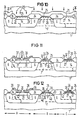
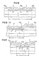
- the source / drain regions 41 of the p-channel transistors C and at the same time the p-doping of the base connection 37 of the bipolar transistor A and the gate electrode 36 are achieved by boron ion implantation with a dose and energy of 4 ⁇ 1015 cm ⁇ 2 and 40 keV generated.
- the n-channel transistor regions B and the emitter terminal 38 of the bipolar transistor A are covered with a photoresist mask.
- the distance emitter / base connection (37, 38) is defined by the spacer oxide 39.
- the circuit arrangement is completed in a known manner by means of contact hole technology, metallization (single-layer or two-layer metallization) and passivation.
- the letters (A, B, C) shown in FIG. 12 mark the area of the bipolar transistor A and the areas of the n-channel transistor B and the p-channel transistor C.
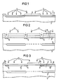
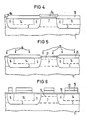
- a p-doped substrate (1) with a specific electrical resistance of 0.02 ohm cm it is also possible to start from a p-doped substrate (1) with a specific electrical resistance of 0.02 ohm cm and to omit the implantation shown in FIG. 1 to produce the buried collector or with a starting material from 20 ohm cm to omit the implantation shown in FIG. 1 and not to apply the epitaxial layer shown in FIG. 3. Saving the buried collector simplifies the process.
Landscapes
- Metal-Oxide And Bipolar Metal-Oxide Semiconductor Integrated Circuits (AREA)
- Bipolar Transistors (AREA)
- Electrodes Of Semiconductors (AREA)
Priority Applications (1)
| Application Number | Priority Date | Filing Date | Title |
|---|---|---|---|
| AT87104507T ATE94688T1 (de) | 1986-07-04 | 1987-03-26 | Integrierte bipolar- und komplementaere mostransistoren auf einem gemeinsamen substrat enthaltende schaltung und verfahren zu ihrer herstellung. |
Applications Claiming Priority (2)
| Application Number | Priority Date | Filing Date | Title |
|---|---|---|---|
| DE3622525 | 1986-07-04 | ||
| DE3622525 | 1986-07-04 |
Publications (3)
| Publication Number | Publication Date |
|---|---|
| EP0250721A2 true EP0250721A2 (fr) | 1988-01-07 |
| EP0250721A3 EP0250721A3 (en) | 1990-05-23 |
| EP0250721B1 EP0250721B1 (fr) | 1993-09-15 |
Family
ID=6304409
Family Applications (1)
| Application Number | Title | Priority Date | Filing Date |
|---|---|---|---|
| EP87104507A Expired - Lifetime EP0250721B1 (fr) | 1986-07-04 | 1987-03-26 | Circuit intégré comprenant sur un substrat commun des transistors bipolaires et des transistors MOS complémentaires et son procédé de fabrication |
Country Status (7)
| Country | Link |
|---|---|
| US (1) | US5100811A (fr) |
| EP (1) | EP0250721B1 (fr) |
| JP (1) | JP2807677B2 (fr) |
| KR (1) | KR950006984B1 (fr) |
| AT (1) | ATE94688T1 (fr) |
| CA (1) | CA1310763C (fr) |
| DE (1) | DE3787407D1 (fr) |
Cited By (9)
| Publication number | Priority date | Publication date | Assignee | Title |
|---|---|---|---|---|
| US4943536A (en) * | 1988-05-31 | 1990-07-24 | Texas Instruments, Incorporated | Transistor isolation |
| EP0403009A1 (fr) * | 1989-06-16 | 1990-12-19 | Koninklijke Philips Electronics N.V. | Méthode de fabrication d'un dispositif semi-conducteur |
| EP0427253A3 (en) * | 1989-11-09 | 1991-09-11 | Kabushiki Kaisha Toshiba | Semiconductor integrated circuit device including bipolar transistors, mos fets and ccd |
| EP0435257A3 (en) * | 1989-12-27 | 1991-10-09 | Oki Electric Industry Co., Ltd. | Fabrication method for bimos semiconductor device with improved speed and reliability |
| DE4139490A1 (de) * | 1991-06-27 | 1993-01-07 | Samsung Electronics Co Ltd | Bicmos-vorrichtung und verfahren zur herstellung derselben |
| US5256582A (en) * | 1989-02-10 | 1993-10-26 | Texas Instruments Incorporated | Method of forming complementary bipolar and MOS transistor having power and logic structures on the same integrated circuit substrate |
| US5288651A (en) * | 1989-11-09 | 1994-02-22 | Kabushiki Kaisha Toshiba | Method of making semiconductor integrated circuit device including bipolar transistors, MOS FETs and CCD |
| US5336911A (en) * | 1988-05-10 | 1994-08-09 | Seiko Epson Corporation | Semiconductor device |
| WO1995023430A1 (fr) * | 1994-02-28 | 1995-08-31 | National Semiconductor Corporation | Structures bipolaires et bichos, et procedes pour leur fabrication |
Families Citing this family (12)
| Publication number | Priority date | Publication date | Assignee | Title |
|---|---|---|---|---|
| JPH01202856A (ja) * | 1988-02-09 | 1989-08-15 | Matsushita Electron Corp | 半導体集積回路の製造方法 |
| JPH025463A (ja) * | 1988-06-24 | 1990-01-10 | Hitachi Ltd | 半導体集積回路装置及びその製造方法 |
| US5318917A (en) * | 1988-11-04 | 1994-06-07 | Matsushita Electric Industrial Co., Ltd. | Method of fabricating semiconductor device |
| US5290714A (en) * | 1990-01-12 | 1994-03-01 | Hitachi, Ltd. | Method of forming semiconductor device including a CMOS structure having double-doped channel regions |
| US6249030B1 (en) * | 1992-12-07 | 2001-06-19 | Hyundai Electronics Industries Co., Ltd. | BI-CMOS integrated circuit |
| DE4308958A1 (de) * | 1993-03-21 | 1994-09-22 | Prema Paezisionselektronik Gmb | Verfahren zur Herstellung von Bipolartransistoren |
| US5652183A (en) * | 1994-01-18 | 1997-07-29 | Matsushita Electric Industrial Co., Ltd. | Method for fabricating semiconductor device containing excessive silicon in metal silicide film |
| US5439833A (en) * | 1994-03-15 | 1995-08-08 | National Semiconductor Corp. | Method of making truly complementary and self-aligned bipolar and CMOS transistor structures with minimized base and gate resistances and parasitic capacitance |
| KR0141165B1 (ko) * | 1995-03-08 | 1998-07-15 | 김광호 | 반도체장치의 트랜지스터 제조방법 |
| JPH09306924A (ja) * | 1996-03-15 | 1997-11-28 | Toshiba Corp | 半導体装置の製造方法 |
| JP3321553B2 (ja) * | 1997-10-08 | 2002-09-03 | 松下電器産業株式会社 | Bi−CMOS集積回路装置の製造方法 |
| JP6070333B2 (ja) * | 2013-03-25 | 2017-02-01 | セイコーエプソン株式会社 | 半導体装置の製造方法 |
Family Cites Families (19)
| Publication number | Priority date | Publication date | Assignee | Title |
|---|---|---|---|---|
| US4074304A (en) * | 1974-10-04 | 1978-02-14 | Nippon Electric Company, Ltd. | Semiconductor device having a miniature junction area and process for fabricating same |
| CH618633A5 (fr) * | 1978-02-07 | 1980-08-15 | Hermes Precisa International | |
| DE3211761A1 (de) * | 1982-03-30 | 1983-10-06 | Siemens Ag | Verfahren zum herstellen von integrierten mos-feldeffekttransistorschaltungen in siliziumgate-technologie mit silizid beschichteten diffusionsgebieten als niederohmige leiterbahnen |
| DE3230077A1 (de) * | 1982-08-12 | 1984-02-16 | Siemens AG, 1000 Berlin und 8000 München | Integrierte bipolar- und mos-transistoren enthaltende halbleiterschaltung auf einem chip und verfahren zu ihrer herstellung |
| JPS5955052A (ja) * | 1982-09-24 | 1984-03-29 | Hitachi Ltd | 半導体集積回路装置の製造方法 |
| US4521952A (en) * | 1982-12-02 | 1985-06-11 | International Business Machines Corporation | Method of making integrated circuits using metal silicide contacts |
| JPS59117150A (ja) * | 1982-12-24 | 1984-07-06 | Hitachi Ltd | 半導体集積回路装置とその製造法 |
| US4554572A (en) * | 1983-06-17 | 1985-11-19 | Texas Instruments Incorporated | Self-aligned stacked CMOS |
| FR2549293B1 (fr) * | 1983-07-13 | 1986-10-10 | Silicium Semiconducteur Ssc | Transistor bipolaire haute frequence et son procede de fabrication |
| US4546536A (en) * | 1983-08-04 | 1985-10-15 | International Business Machines Corporation | Fabrication methods for high performance lateral bipolar transistors |
| JPS6058644A (ja) * | 1983-09-12 | 1985-04-04 | Toshiba Corp | 半導体装置 |
| JPS6080267A (ja) * | 1983-10-07 | 1985-05-08 | Toshiba Corp | 半導体集積回路装置の製造方法 |
| FR2555365B1 (fr) * | 1983-11-22 | 1986-08-29 | Efcis | Procede de fabrication de circuit integre avec connexions de siliciure de tantale et circuit integre realise selon ce procede |
| JPS61110457A (ja) * | 1984-11-05 | 1986-05-28 | Nec Corp | 半導体装置 |
| JPH0666425B2 (ja) * | 1984-12-07 | 1994-08-24 | 日本電信電話株式会社 | 複合型半導体装置 |
| ATE59917T1 (de) * | 1985-09-13 | 1991-01-15 | Siemens Ag | Integrierte bipolar- und komplementaere mostransistoren auf einem gemeinsamen substrat enthaltende schaltung und verfahren zu ihrer herstellung. |
| US4929992A (en) * | 1985-09-18 | 1990-05-29 | Advanced Micro Devices, Inc. | MOS transistor construction with self aligned silicided contacts to gate, source, and drain regions |
| JPH0628296B2 (ja) * | 1985-10-17 | 1994-04-13 | 日本電気株式会社 | 半導体装置の製造方法 |
| US4764482A (en) * | 1986-11-21 | 1988-08-16 | General Electric Company | Method of fabricating an integrated circuit containing bipolar and MOS transistors |
-
1987
- 1987-03-26 AT AT87104507T patent/ATE94688T1/de not_active IP Right Cessation
- 1987-03-26 EP EP87104507A patent/EP0250721B1/fr not_active Expired - Lifetime
- 1987-03-26 DE DE87104507T patent/DE3787407D1/de not_active Expired - Lifetime
- 1987-06-29 JP JP62165141A patent/JP2807677B2/ja not_active Expired - Lifetime
- 1987-07-03 CA CA000541208A patent/CA1310763C/fr not_active Expired - Lifetime
- 1987-07-04 KR KR1019870007128A patent/KR950006984B1/ko not_active Expired - Fee Related
-
1990
- 1990-12-21 US US07/632,411 patent/US5100811A/en not_active Expired - Lifetime
Cited By (12)
| Publication number | Priority date | Publication date | Assignee | Title |
|---|---|---|---|---|
| US5336911A (en) * | 1988-05-10 | 1994-08-09 | Seiko Epson Corporation | Semiconductor device |
| US4943536A (en) * | 1988-05-31 | 1990-07-24 | Texas Instruments, Incorporated | Transistor isolation |
| US5256582A (en) * | 1989-02-10 | 1993-10-26 | Texas Instruments Incorporated | Method of forming complementary bipolar and MOS transistor having power and logic structures on the same integrated circuit substrate |
| EP0403009A1 (fr) * | 1989-06-16 | 1990-12-19 | Koninklijke Philips Electronics N.V. | Méthode de fabrication d'un dispositif semi-conducteur |
| US4988633A (en) * | 1989-06-16 | 1991-01-29 | U.S. Philips Corporation | Method of manufacturing a semiconductor Bi-CMOS device |
| EP0427253A3 (en) * | 1989-11-09 | 1991-09-11 | Kabushiki Kaisha Toshiba | Semiconductor integrated circuit device including bipolar transistors, mos fets and ccd |
| US5288651A (en) * | 1989-11-09 | 1994-02-22 | Kabushiki Kaisha Toshiba | Method of making semiconductor integrated circuit device including bipolar transistors, MOS FETs and CCD |
| EP0435257A3 (en) * | 1989-12-27 | 1991-10-09 | Oki Electric Industry Co., Ltd. | Fabrication method for bimos semiconductor device with improved speed and reliability |
| DE4139490A1 (de) * | 1991-06-27 | 1993-01-07 | Samsung Electronics Co Ltd | Bicmos-vorrichtung und verfahren zur herstellung derselben |
| WO1995023430A1 (fr) * | 1994-02-28 | 1995-08-31 | National Semiconductor Corporation | Structures bipolaires et bichos, et procedes pour leur fabrication |
| US5543653A (en) * | 1994-02-28 | 1996-08-06 | National Semiconductor Corporation | Bipolar and BiCMOS structures |
| US5580798A (en) * | 1994-02-28 | 1996-12-03 | National Semiconductor Corporation | Method of fabricating bipolar transistor having a guard ring |
Also Published As
| Publication number | Publication date |
|---|---|
| ATE94688T1 (de) | 1993-10-15 |
| JP2807677B2 (ja) | 1998-10-08 |
| KR880002245A (ko) | 1988-04-29 |
| CA1310763C (fr) | 1992-11-24 |
| US5100811A (en) | 1992-03-31 |
| EP0250721B1 (fr) | 1993-09-15 |
| KR950006984B1 (ko) | 1995-06-26 |
| JPS6328060A (ja) | 1988-02-05 |
| EP0250721A3 (en) | 1990-05-23 |
| DE3787407D1 (de) | 1993-10-21 |
Similar Documents
| Publication | Publication Date | Title |
|---|---|---|
| EP0219641B1 (fr) | Circuit intégré comprenant des transistors bipolaires et MOS complémentaires sur un substrat commun et méthode pour sa fabrication | |
| EP0226892B1 (fr) | Procédé pour la fabrication de transistors bipolaires et MOS-complémentaires sur un substrat commun en silicium | |
| DE3105118C2 (de) | Verfahren zur Herstellung einer integrierten Schaltung mit komplementären bipolaren Transistoren und komplementären Isolierschicht-Gate-Feldeffekttransistoren auf einem gemeinsamen Substrat | |
| EP0250721B1 (fr) | Circuit intégré comprenant sur un substrat commun des transistors bipolaires et des transistors MOS complémentaires et son procédé de fabrication | |
| EP0256315B1 (fr) | Circuit intégré contenant des transistors bipolaires et de type CMOS sur le même substrat et son procédé de fabrication | |
| EP0227970B1 (fr) | Procédé de fabrication simultanée de transistors bipolaires auto-alignés et de transistors de type MOS complémentaires sur un substrat en silicium commun | |
| EP0204979B1 (fr) | Procédé de fabrication simultanée des transistors de type MOS complémentaires et bipolaires sur le même substrat en silicium | |
| EP0244607B1 (fr) | Méthode pour fabriquer des transistors CMOS optimisés à effet de champ en technologie VLSI | |
| DE68922817T2 (de) | Halbleiteranordnungen mit eng beabstandeten Gebieten, hergestellt unter Verwendung eines selbstausrichtenden Umkehrbildverfahrens. | |
| DE68926224T2 (de) | Verfahren zum Herstellen einer BICMOS-Anordnung | |
| DE69032735T2 (de) | Verfahren zum Herstellen von Hochspannungs- und Niederspannungs-CMOS-Transistoren in einem einzigen integrierten Schaltungs-Chip | |
| DE3019850C2 (fr) | ||
| DE69128568T2 (de) | Kontaktstrukturen für Halbleiteranordnungen und Verfahren zu ihrer Herstellung | |
| US6362038B1 (en) | Low and high voltage CMOS devices and process for fabricating same | |
| EP0247386B1 (fr) | Transistor latéral | |
| EP0272433B1 (fr) | Circuit intégré semi-conducteur avec des résistances de charge arrangées sur les régions des oxydes de champ séparant les roues actives des transistors et son mode de fabrication | |
| EP0020998B1 (fr) | Procédé de fabrication d'un transistor bipolaire comprenant une zône d'émetteur à implantation ionique | |
| EP0071665B1 (fr) | Procédé pour la fabrication d'un circuit intégré à corps solide et monolithique ayant au moins un transistor bipolaire plan | |
| EP0248988A1 (fr) | Procédé pour fabriquer des circuits à transistors complémentaires à effet de champ du type MOS à haute intégration | |
| EP0293641B1 (fr) | Procédé de fabrication à un transistor bipolaire entièrement auto-aligné | |
| EP0232497B1 (fr) | Procédé pour la fabrication simultanée de transistors bipolaires et MOS-complémentaires sur un substrat commun en silicium | |
| DE69020708T2 (de) | Verfahren zur Herstellung von biMOS-Halbleiterbauelementen mit verbesserter Schnelligkeit und Zuverlässigkeit. | |
| DE3850847T2 (de) | Selbstjustierter Polysiliziumemitter und Kontaktstruktur für Hochleistungsbipolartransistor. | |
| EP0226890B1 (fr) | Procédé de fabrication de structures de transistors bipolaires auto-alignés à résistance de base réduite | |
| DE3022565A1 (de) | Halbleiteranordnung |
Legal Events
| Date | Code | Title | Description |
|---|---|---|---|
| PUAI | Public reference made under article 153(3) epc to a published international application that has entered the european phase |
Free format text: ORIGINAL CODE: 0009012 |
|
| AK | Designated contracting states |
Kind code of ref document: A2 Designated state(s): AT DE FR GB IT NL SE |
|
| PUAL | Search report despatched |
Free format text: ORIGINAL CODE: 0009013 |
|
| AK | Designated contracting states |
Kind code of ref document: A3 Designated state(s): AT DE FR GB IT NL SE |
|
| 17P | Request for examination filed |
Effective date: 19900919 |
|
| 17Q | First examination report despatched |
Effective date: 19920709 |
|
| GRAA | (expected) grant |
Free format text: ORIGINAL CODE: 0009210 |
|
| AK | Designated contracting states |
Kind code of ref document: B1 Designated state(s): AT DE FR GB IT NL SE |
|
| REF | Corresponds to: |
Ref document number: 94688 Country of ref document: AT Date of ref document: 19931015 Kind code of ref document: T |
|
| REF | Corresponds to: |
Ref document number: 3787407 Country of ref document: DE Date of ref document: 19931021 |
|
| ITF | It: translation for a ep patent filed | ||
| GBT | Gb: translation of ep patent filed (gb section 77(6)(a)/1977) |
Effective date: 19931122 |
|
| ET | Fr: translation filed | ||
| PLBE | No opposition filed within time limit |
Free format text: ORIGINAL CODE: 0009261 |
|
| STAA | Information on the status of an ep patent application or granted ep patent |
Free format text: STATUS: NO OPPOSITION FILED WITHIN TIME LIMIT |
|
| 26N | No opposition filed | ||
| EAL | Se: european patent in force in sweden |
Ref document number: 87104507.6 |
|
| REG | Reference to a national code |
Ref country code: GB Ref legal event code: IF02 |
|
| PGFP | Annual fee paid to national office [announced via postgrant information from national office to epo] |
Ref country code: NL Payment date: 20040227 Year of fee payment: 18 |
|
| PGFP | Annual fee paid to national office [announced via postgrant information from national office to epo] |
Ref country code: SE Payment date: 20040302 Year of fee payment: 18 |
|
| PGFP | Annual fee paid to national office [announced via postgrant information from national office to epo] |
Ref country code: GB Payment date: 20040303 Year of fee payment: 18 Ref country code: AT Payment date: 20040303 Year of fee payment: 18 |
|
| PGFP | Annual fee paid to national office [announced via postgrant information from national office to epo] |
Ref country code: FR Payment date: 20040310 Year of fee payment: 18 |
|
| PG25 | Lapsed in a contracting state [announced via postgrant information from national office to epo] |
Ref country code: IT Free format text: LAPSE BECAUSE OF NON-PAYMENT OF DUE FEES;WARNING: LAPSES OF ITALIAN PATENTS WITH EFFECTIVE DATE BEFORE 2007 MAY HAVE OCCURRED AT ANY TIME BEFORE 2007. THE CORRECT EFFECTIVE DATE MAY BE DIFFERENT FROM THE ONE RECORDED. Effective date: 20050326 Ref country code: GB Free format text: LAPSE BECAUSE OF NON-PAYMENT OF DUE FEES Effective date: 20050326 Ref country code: AT Free format text: LAPSE BECAUSE OF NON-PAYMENT OF DUE FEES Effective date: 20050326 |
|
| PG25 | Lapsed in a contracting state [announced via postgrant information from national office to epo] |
Ref country code: SE Free format text: LAPSE BECAUSE OF NON-PAYMENT OF DUE FEES Effective date: 20050327 |
|
| PG25 | Lapsed in a contracting state [announced via postgrant information from national office to epo] |
Ref country code: NL Free format text: LAPSE BECAUSE OF NON-PAYMENT OF DUE FEES Effective date: 20051001 |
|
| EUG | Se: european patent has lapsed | ||
| GBPC | Gb: european patent ceased through non-payment of renewal fee |
Effective date: 20050326 |
|
| PG25 | Lapsed in a contracting state [announced via postgrant information from national office to epo] |
Ref country code: FR Free format text: LAPSE BECAUSE OF NON-PAYMENT OF DUE FEES Effective date: 20051130 |
|
| NLV4 | Nl: lapsed or anulled due to non-payment of the annual fee |
Effective date: 20051001 |
|
| REG | Reference to a national code |
Ref country code: FR Ref legal event code: ST Effective date: 20051130 |
|
| PGFP | Annual fee paid to national office [announced via postgrant information from national office to epo] |
Ref country code: DE Payment date: 20060516 Year of fee payment: 20 |