EP0250832A2 - Hohlraumschlitzantenne - Google Patents
Hohlraumschlitzantenne Download PDFInfo
- Publication number
- EP0250832A2 EP0250832A2 EP87107358A EP87107358A EP0250832A2 EP 0250832 A2 EP0250832 A2 EP 0250832A2 EP 87107358 A EP87107358 A EP 87107358A EP 87107358 A EP87107358 A EP 87107358A EP 0250832 A2 EP0250832 A2 EP 0250832A2
- Authority
- EP
- European Patent Office
- Prior art keywords
- antenna
- slot
- conductive sheet
- cavity
- electrically
- Prior art date
- Legal status (The legal status is an assumption and is not a legal conclusion. Google has not performed a legal analysis and makes no representation as to the accuracy of the status listed.)
- Withdrawn
Links
- 239000000463 material Substances 0.000 claims abstract description 17
- 230000005540 biological transmission Effects 0.000 claims abstract description 7
- 230000000694 effects Effects 0.000 claims abstract description 6
- 229910052729 chemical element Inorganic materials 0.000 claims 1
- 230000009467 reduction Effects 0.000 abstract description 10
- 239000004020 conductor Substances 0.000 abstract description 5
- 238000006722 reduction reaction Methods 0.000 description 9
- 239000003990 capacitor Substances 0.000 description 7
- XEEYBQQBJWHFJM-UHFFFAOYSA-N Iron Chemical compound [Fe] XEEYBQQBJWHFJM-UHFFFAOYSA-N 0.000 description 6
- 238000010276 construction Methods 0.000 description 5
- 230000005855 radiation Effects 0.000 description 5
- 238000000034 method Methods 0.000 description 4
- 230000010287 polarization Effects 0.000 description 4
- 230000001681 protective effect Effects 0.000 description 4
- 229910052742 iron Inorganic materials 0.000 description 3
- 238000005549 size reduction Methods 0.000 description 3
- RYGMFSIKBFXOCR-UHFFFAOYSA-N Copper Chemical compound [Cu] RYGMFSIKBFXOCR-UHFFFAOYSA-N 0.000 description 2
- 239000004593 Epoxy Substances 0.000 description 2
- GWEVSGVZZGPLCZ-UHFFFAOYSA-N Titan oxide Chemical compound O=[Ti]=O GWEVSGVZZGPLCZ-UHFFFAOYSA-N 0.000 description 2
- 229910052782 aluminium Inorganic materials 0.000 description 2
- XAGFODPZIPBFFR-UHFFFAOYSA-N aluminium Chemical compound [Al] XAGFODPZIPBFFR-UHFFFAOYSA-N 0.000 description 2
- 239000000919 ceramic Substances 0.000 description 2
- 229910052802 copper Inorganic materials 0.000 description 2
- 239000010949 copper Substances 0.000 description 2
- 239000003989 dielectric material Substances 0.000 description 2
- 239000011152 fibreglass Substances 0.000 description 2
- 229910052751 metal Inorganic materials 0.000 description 2
- 239000002184 metal Substances 0.000 description 2
- 230000002093 peripheral effect Effects 0.000 description 2
- 230000035699 permeability Effects 0.000 description 2
- 239000000843 powder Substances 0.000 description 2
- 239000012780 transparent material Substances 0.000 description 2
- PNEYBMLMFCGWSK-UHFFFAOYSA-N Alumina Chemical compound [O-2].[O-2].[O-2].[Al+3].[Al+3] PNEYBMLMFCGWSK-UHFFFAOYSA-N 0.000 description 1
- 229910052582 BN Inorganic materials 0.000 description 1
- PZNSFCLAULLKQX-UHFFFAOYSA-N Boron nitride Chemical compound N#B PZNSFCLAULLKQX-UHFFFAOYSA-N 0.000 description 1
- OKTJSMMVPCPJKN-UHFFFAOYSA-N Carbon Chemical compound [C] OKTJSMMVPCPJKN-UHFFFAOYSA-N 0.000 description 1
- JOYRKODLDBILNP-UHFFFAOYSA-N Ethyl urethane Chemical compound CCOC(N)=O JOYRKODLDBILNP-UHFFFAOYSA-N 0.000 description 1
- 241001101998 Galium Species 0.000 description 1
- 239000004793 Polystyrene Substances 0.000 description 1
- 230000002411 adverse Effects 0.000 description 1
- 238000013459 approach Methods 0.000 description 1
- 238000005452 bending Methods 0.000 description 1
- 229910052799 carbon Inorganic materials 0.000 description 1
- 238000007796 conventional method Methods 0.000 description 1
- 238000009826 distribution Methods 0.000 description 1
- 230000005684 electric field Effects 0.000 description 1
- 238000005530 etching Methods 0.000 description 1
- 230000005284 excitation Effects 0.000 description 1
- 239000000945 filler Substances 0.000 description 1
- 239000006260 foam Substances 0.000 description 1
- 238000004519 manufacturing process Methods 0.000 description 1
- 239000003550 marker Substances 0.000 description 1
- 239000012811 non-conductive material Substances 0.000 description 1
- TWNQGVIAIRXVLR-UHFFFAOYSA-N oxo(oxoalumanyloxy)alumane Chemical compound O=[Al]O[Al]=O TWNQGVIAIRXVLR-UHFFFAOYSA-N 0.000 description 1
- 238000000206 photolithography Methods 0.000 description 1
- 229920002223 polystyrene Polymers 0.000 description 1
- 239000011347 resin Substances 0.000 description 1
- 229920005989 resin Polymers 0.000 description 1
- 239000002210 silicon-based material Substances 0.000 description 1
- 229920002050 silicone resin Polymers 0.000 description 1
- 239000000758 substrate Substances 0.000 description 1
- 239000004408 titanium dioxide Substances 0.000 description 1
- 239000013598 vector Substances 0.000 description 1
Images


Classifications
-
- H—ELECTRICITY
- H01—ELECTRIC ELEMENTS
- H01Q—ANTENNAS, i.e. RADIO AERIALS
- H01Q19/00—Combinations of primary active antenna elements and units with secondary devices, e.g. with quasi-optical devices, for giving the antenna a desired directional characteristic
- H01Q19/06—Combinations of primary active antenna elements and units with secondary devices, e.g. with quasi-optical devices, for giving the antenna a desired directional characteristic using refracting or diffracting devices, e.g. lens
- H01Q19/09—Combinations of primary active antenna elements and units with secondary devices, e.g. with quasi-optical devices, for giving the antenna a desired directional characteristic using refracting or diffracting devices, e.g. lens wherein the primary active element is coated with or embedded in a dielectric or magnetic material
-
- H—ELECTRICITY
- H01—ELECTRIC ELEMENTS
- H01Q—ANTENNAS, i.e. RADIO AERIALS
- H01Q13/00—Waveguide horns or mouths; Slot antennas; Leaky-waveguide antennas; Equivalent structures causing radiation along the transmission path of a guided wave
- H01Q13/10—Resonant slot antennas
- H01Q13/18—Resonant slot antennas the slot being backed by, or formed in boundary wall of, a resonant cavity ; Open cavity antennas
Definitions
- the present invention generally relates to antenna structures and, more particularly, is concerned with a slot antenna backed by an electrically small cavity and tuned to resonance primarily by dielectric loading placed over the slot and secondarily by variable capacitance placed symmetrically across the slot which combination results in reduction of the physical size and increase in the gain and efficiency of the antenna.
- Cavity-backed slot antennas are well known in the prior art. Traditionally, they are composed of a metal surface backed by an energized resonant cavity and having a slot through which energy is radiated directionally. Representative of the prior art are the cavity-backed slot antennas disclosed in U.S. Patents to Lindenblad (2,570,824), Fales (2,684,444), Turner (2,863,l45), Baldwin (2,885,676), Charman (3,056,l30), Harris et al (3,550,l4l), Monser (4,l32,995), Sanford (4,242,685) and Schiavone (4,367,475).
- radiating slot antennas are particularly useful in applications where the antenna must conform to an external surface so as to not interfere with the desired characteristics of the surface.
- a cavity-backed slot antenna is advantageously used in conjunction with an aircraft wing or fuselage since it will not adversely affect the aerodynamics of the aircraft surface.
- the resonant cavity which backs the radiating slot is typically provided on the interior side of the aerodynamic surface in order to limit radiation of energy to the exterior side thereof. To accommodate the cavity there must be unused space available. But, in most applications, interior space is at a premium. Therefore, one basic objective in cavity-backed slot antenna design must be to minimize the physical size of the cavity to the extent feasible without unduly sacrificing the performance characteristics of the antenna.
- an electrically conductive plate is disposed within the cavity and spaced from all of its internal walls so as to lengthen the effective electrical resonant dimensions of the cavity for a given physical size.
- the resonant cavity can thus be smaller in size for a given frequency of operation.
- the present invention provides a cavity-backed slot antenna designed to satisfy the aforementioned needs.
- An electrically small (non-resonant) cavity is used to restrict radiation to one direction from the slot and the small size permits mounting in areas where spaced is at a premium.
- Size reduction of the slot antenna cavity is achieved primarily through the use of a high dielectric constant layer placed at the radiating portion of the antenna.
- the advantage of dielectric loading versus the methods used previously, such as lumped reactance elements, is that it is more efficient at higher frequencies as compared to the other methods of loading.
- variable capacitors are employed to permit "fine tuning", that is, to make small resonant frequency adjustments such as might become necessary to compensate for small changes in material properties and dimensions during production.
- "gross tuning" of the antenna that is, major frequency reduction is accomplished by the layer of dielectric material. Tuning the antenna to resonance for any given cavity size and slot length is achieved primarily by dielectric loading placed over the slot and secondarily by variable capacitance placed symmetrically across the slot. This combination of improvements introduced into a cavity-backed slot antenna results in reduction of the physical size and resonant frequency for any given slot length and cavity size. In addition, the improved antenna exhibits higher gain and efficiency relative to other antennas designed for the same frequency, pattern coverage, polarization and size.
- the present invention relates to an antenna which comprises: (a) an electrically conductive sheet having a cavity-backed directionally-radiating elongated slot; (b) a dielectric layer composed of material having a dielectric constant of ten or more coupled to the conductive sheet so as to overlie the slot to effect reduction of the resonant frequency of the antenna; and (c) r.f. transmission means electrically coupled to the conductive sheet across and on opposite sides of the slot and adapted to carry r.f. energy.
- the antenna includes electrically reactive means mounted across the slot and electrically coupled to the conductive sheet on opposite sides of the slot and being variable for fine tuning the resonant frequency of the antenna.
- the present invention is directed to a cavity-backed slot antenna which comprises: (a) an electrically conductive sheet having an elongated slot of a given length formed therein; (b) an electrically conductive housing electrically connected to the conductive sheet and defining a cavity of a given size therein which encloses the slot at one side of the sheet: (c) a dielectric layer composed of material having a high dielectric constant, the dielectric layer being disposed over at least the slot defined in the conductive sheet so as to effect a reduction of the resonant frequency of the antenna below that otherwise associated with the given cavity size and slot length permitting the antenna to be characterized as electrically small; (d) transmission means electrically coupled to the conductive sheet across and on opposite sides of the slot and adapted to carry r.f. energy; and (e) electrically reactive means mounted across the slot and electrically coupled to the conductive sheet on opposite sides of the slot and being adjustable for fine tuning the resonant frequency of
- the high dielectric constant of the dielectric layer is between approximately l0 and 80, and preferably about 20, and the layer has a thickness between about 40 and 80 mils.
- the depth of the cavity is substantially less than one-quarter wavelength.
- the elongated slot is contained within the perimeter of the conductive sheet and can have a configuration in the shape of an unconnected square, triangle or circle, or of a straight line.
- the reactive means is in the form of a pair of high Q capacitive elements mounted across the slot and electrically coupled to the conductive sheet on opposite sides of the slot and at symmetrical locations therealong.
- the capacitive elements are variable for fine tuning the resonant frequency of the antenna.
- the antenna includes a protective cover of electrically transparent material overlying the dielectric layer.
- the conductive sheet includes a dielectric plate composed of material having a dielectric constant of less than three which extends across and is connected to the top of the housing, and an electrically conductive layer covering an interior side of the dielectric plate and electrically contacting the housing.
- the conductive layer has the slot defined therein so as to be wholly contained within its perimeter.
- the antenna l0 is electrically small and adapted to provide a cardioid-shaped radiating r.f. pattern.
- the antenna l0 includes an electrically conductive housing l2, an electrically conductive sheet in the form of a printed circuit board l4, a dielectric layer l6 and a protective cover l8.
- a non-conductive slot 20 formed in the p.c. board l4 electrically reactive devices in the form of a pair of variable capacitors 22, and a r.f. transmission line in the form of a coaxial cable 26 are included in the antenna l0.
- the housing l2 composed of electrically conductive material such as copper or aluminum and fabricated using conventional construction techniques, is rectangular shaped in the embodiment illustrated in Fig. l, being closed at its side 26 and bottom 28 and open at its top 30 so as to define a cavity 32 of a desired given size therein.
- the cavity 32 has a depth substantially less than one-quarter wavelength.
- the depth of the cavity 32 is .034 wavelength in free space.
- the coaxial cable 26 which extends into the cavity 32 is anchored to the bottom 28 of the housing l2 by an r.f. connector 34.
- a series of internally threaded holes 36 are tapped into an annular mounting flange 38 which extends about the top 30 of the housing l2.
- the holes 36 are located along and outwardly of an endless recess 40 formed in the flange 38 at its inner edge which bounds the top of the cavity 32.
- the p.c. board l4 is dimensioned to snugly fit into the recess 40 in the housing top mounting flange 38.
- the board l4 includes a dielectric substrate or plate 42 and an electrically conductive layer 44.
- the dielectric plate 42 is composed of any suitable dielectric material having a dielectric constant of less than three, for example Teflon-Fiberglass material having a dielectric constant of 2.54.
- the conductive layer 44 for example a copper clad, is formed on the interior side of the plate 42 by any suitable technique, for instance using known photolithography.
- the conductive layer 44 extends along the interior side of the plate 42 from edge-to-edge so as to make electrical contact about its peripheral edge 46 with the conductive housing l2 when the board l4 is seated in the housing recess 40, as seen in Fig. 2, closing the top of the housing l2 and the cavity 32 formed therein.
- the conductive layer 44 covers the entire bottom or interior side of the dielectric plate 42 except for the elongated slot 20 formed thereon by any suitable conventional technique, such as by etching away the material of the conductive layer 44.
- the slot 20 is represented by the absence of conductive material in the desired configuration on interior side of the plate 42. It is not necessary that the slot 20 be formed completely through the p.c. board l4, only that any portion of the board bridging the slot be electrically non-conductive. Since there is no electrically conductive material deposited on the exterior side of the p.c. board l4, the only material bridging the slot 20 is the non-conductive material of the dielectric plate 42. At this point it should be pointed out that while the p.c.
- board l4 is usefully employed for creating the slot 20, it is not necessary that a p.c. board be used and thus the make-up of the antenna l0 is not so limited. All that is required is to have a slot cut into any good electrical conductor, for instance an aluminum plate or sheet. However, if this is done, some additional support would be required to provide mechanical stability to the center of the metal sheet.
- the slot 20 is contained within the perimeter of the conductive layer 44 and furthermore enclosed within the top perimeter of the cavity 32 when the p.c. board l4 is seated in the housing recess 40.
- the unconnected square configuration of the slot 20, depicted in Figs. l and 3, is designed to provide a cardioid-shaped radiation pattern with the polarization parallel to the plane of the slot 20.
- the electric field vectors across the slot 20 have a sinusoidal amplitude distribution along the slot 20 with minimum amplitude occurring at each end of the slot.
- the slot 20 has a length of 0.4 wavelength in dielectric and a width of 0.0l wavelength in dielectric.
- the dielectric layer l6 and protective cover l8 have respective holes 48, 50 holes drilled along their peripheral edges for receiving screws 52 to thread into the holes 36 in the housing flange 38 for securing the layer l6 and cover l8 to the top of housing l2.
- the radome or protective cover l8 is composed of an electrically transparent material, such as a thin sheet of Fiberglass-epoxy or Teflon-Fiberglass, and overlies the dielectric layer l6.
- the cover l8 can either be separate from the dielectric layer l6, as seen in Fig. l, or alternatively bonded to its outer side.
- the dielectric layer l6 is composed of material having a dielectric constant ⁇ r of ten or greater, more specifically between ten and eighty and preferably approximately twenty with a permeability ⁇ r of approximately three.
- Suitable materials for forming the dielectric layer l6 are alumina ceramic, silicone resin/ceramic powder-filled, boron nitride, galium arsenide, aluminum oxide, and cross linked polystyrene/ceramic powder-filled. Also, an iron loaded silicon based material can be used.
- base materials or resins could be used such as epoxy, urethane, foams, etc., with fillers such as carbon/iron, titanium dioxide, and hollow iron spheres to achieve dielectric constants from l0 to 30 or higher with relatively low loss tangeants.
- the reduction in the physical size of the antenna cavity 32 for a given resonant frequency is achieved through loading the slot 20 with the relatively high dielectric constant material of the dielectric layer l6. It is the high dielectric constant of the material that directly affects the size reduction of the antenna. While the thickness of the dielectric layer l6 depends on the dielectric constant and permeability of the material used, in one example the dielectric layer l6 has a thickness between about 40 and 80 mils. The dielectric layer l6 is disposed on the exterior side of the p.c. board l4.
- the antenna l0 In such position, it is disposed over the slot 20 defined in the conductive layer 44 of the board l4 so as to effect a reduction of the resonant frequency of the antenna below that otherwise associated with the particular given cavity size and slot length. It is this effect which permits the antenna l0 to be characterized as electrically small, that is small or undersized compared to its wavelength dimension and to use a non-resonant cavity 32 to restrict radiation to one direction from the slot 20. As seen in the modified construction of Fig. 7, the dielectric layer l6 ⁇ need not cover the entire p.c. board l4 ⁇ , but only at least cover the slot 20 ⁇ formed therein, in the area of highest E field concentration.
- variable capacitors 22 placed symmetrically across the slot 20. As seen in Figs. 2 and 3, the capacitors 22 are mounted across the slot 20 and electrically coupled to the conductive layer 44 immediately on opposite sides of slot.
- the small variable capacitors 22 provide fine tuning of the resonant frequency of the antenna l0 and can be used to compensate for variations in material properties and dimensions from one antenna to the next.
- the symmetrical location of the capacitors 22 is essential for the desired radiation pattern and polarization.
- Excitation and impedance matching is readily achieved through location of the transmission line in the form of coaxial cable 24 across the slot 20 at a point where the slot impedance matches the characteristic impedance of the transmission line, i.e., of the cable.
- the short circuit across the gap between the two ends 54 of the slot 20 is used to force a low impedance at some point along the slot.
- the impedance increases sinusoidally either direction away from the short circuit gap and reaches a maximum at the center of the slot length.
- the antenna l0 useful in one application as a marker beacon antenna, exhibits higher gain and efficiency relative to other antennas designed for the same frequency, pattern coverage, polarization and size.
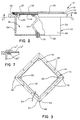
- Figs. 4 to 6 illustrate alternative configurations of the improved cavity-backed slot antenna of the present invention wherein the elongated slot takes other geometric shapes.
- the variable capacitors 22 and the coaxial cable 24 are the same as in the Fig. 2 embodiment.
- the elongated slot 56 is contained within the perimeter of the conductive layer 58 and has a configuration in the shape of an unconnected circle.
- the slot 60 is contained within the perimeter of the conductive layer 62 but now has a configuration in the shape of a straight line.
- the elongated slot 64 is contained within the perimeter of the conductive layer 66 and now has a configuration in the shape of an unconnected triangle.
Landscapes
- Waveguide Aerials (AREA)
- Details Of Aerials (AREA)
Applications Claiming Priority (2)
| Application Number | Priority Date | Filing Date | Title |
|---|---|---|---|
| US06/877,071 US4733245A (en) | 1986-06-23 | 1986-06-23 | Cavity-backed slot antenna |
| US877071 | 1986-06-23 |
Publications (2)
| Publication Number | Publication Date |
|---|---|
| EP0250832A2 true EP0250832A2 (de) | 1988-01-07 |
| EP0250832A3 EP0250832A3 (de) | 1990-03-21 |
Family
ID=25369185
Family Applications (1)
| Application Number | Title | Priority Date | Filing Date |
|---|---|---|---|
| EP87107358A Withdrawn EP0250832A3 (de) | 1986-06-23 | 1987-05-20 | Hohlraumschlitzantenne |
Country Status (2)
| Country | Link |
|---|---|
| US (1) | US4733245A (de) |
| EP (1) | EP0250832A3 (de) |
Cited By (10)
| Publication number | Priority date | Publication date | Assignee | Title |
|---|---|---|---|---|
| GB2248522A (en) * | 1990-10-01 | 1992-04-08 | Secr Defence | Slot antenna with dielectric coupling elements |
| FR2669777A1 (fr) * | 1990-11-27 | 1992-05-29 | Thomson Trt Defense | Antenne du type guide d'ondes a fentes associee a une paroi. |
| EP0649185A1 (de) * | 1993-08-20 | 1995-04-19 | Texas Instruments Incorporated | Antennen |
| FR2736470A1 (fr) * | 1990-11-13 | 1997-01-10 | Bony Gerard | Procede pour la conception d'une antenne hyperfrequence protegee a surface rayonnante horizontale et antennes realisees selon ce procede |
| RU2133530C1 (ru) * | 1998-01-20 | 1999-07-20 | Научно-производственное предприятие "Полет" | Невыступающая кольцевая щелевая антенна |
| WO1999048168A1 (de) * | 1998-03-19 | 1999-09-23 | Honeywell Ag | Elektrische unterputz-installationseinheit mit antenne |
| EP0991135A1 (de) * | 1998-10-02 | 2000-04-05 | Thomson-Csf | Selektive Antenne mit Frequenzumschaltung |
| EP2165385A4 (de) * | 2007-04-10 | 2013-01-23 | Nokia Corp | Antennenanordnung und antennengehäuse |
| US8711044B2 (en) | 2009-11-12 | 2014-04-29 | Nokia Corporation | Antenna arrangement and antenna housing |
| WO2016097362A1 (fr) * | 2014-12-19 | 2016-06-23 | Commissariat A L'energie Atomique Et Aux Energies Alternatives | Antenne fil-plaque ayant un toit capacitif incorporant une fente entre la sonde d'alimentation et le fil de court-circuit |
Families Citing this family (44)
| Publication number | Priority date | Publication date | Assignee | Title |
|---|---|---|---|---|
| US6181277B1 (en) * | 1987-04-08 | 2001-01-30 | Raytheon Company | Microstrip antenna |
| JP2735669B2 (ja) | 1990-03-02 | 1998-04-02 | 株式会社エイ・ティ・アール光電波通信研究所 | 空胴付スロットアンテナ |
| US5245745A (en) * | 1990-07-11 | 1993-09-21 | Ball Corporation | Method of making a thick-film patch antenna structure |
| US5202697A (en) * | 1991-01-18 | 1993-04-13 | Cubic Defense Systems, Inc. | Low-profile steerable cardioid antenna |
| KR100312364B1 (ko) | 1997-05-30 | 2001-12-28 | 가나이 쓰도무 | 동조형 슬롯안테나 |
| US6160522A (en) * | 1998-04-02 | 2000-12-12 | L3 Communications Corporation, Randtron Antenna Systems Division | Cavity-backed slot antenna |
| US6643989B1 (en) * | 1999-02-23 | 2003-11-11 | Renke Bienert | Electric flush-mounted installation unit with an antenna |
| US6150989A (en) * | 1999-07-06 | 2000-11-21 | Sky Eye Railway Services International Inc. | Cavity-backed slot antenna resonating at two different frequencies |
| JP3725766B2 (ja) * | 1999-07-19 | 2005-12-14 | 株式会社日立国際電気 | キャビティ付きスロットアレーアンテナ |
| US6304226B1 (en) * | 1999-08-27 | 2001-10-16 | Raytheon Company | Folded cavity-backed slot antenna |
| BR0109773A (pt) * | 2000-04-04 | 2003-01-21 | Huber+Suhner Ag | Antena de comunicação de banda larga |
| TW529782U (en) * | 2001-08-03 | 2003-04-21 | Hon Hai Prec Ind Co Ltd | Antenna module with opened groove |
| DE10141583B4 (de) * | 2001-08-24 | 2014-02-13 | Heinz Lindenmeier | Antennenanordnung in der Apertur einer elektrisch leitenden Fahrzeugkarosserie |
| US6646614B2 (en) | 2001-11-07 | 2003-11-11 | Harris Corporation | Multi-frequency band antenna and related methods |
| US20080068818A1 (en) * | 2006-09-19 | 2008-03-20 | Jinwoo Choi | Method and apparatus for providing ultra-wide band noise isolation in printed circuit boards |
| US20090153412A1 (en) * | 2007-12-18 | 2009-06-18 | Bing Chiang | Antenna slot windows for electronic device |
| US8174452B2 (en) * | 2008-09-25 | 2012-05-08 | Apple Inc. | Cavity antenna for wireless electronic devices |
| US8125394B2 (en) * | 2009-01-20 | 2012-02-28 | Apple Inc. | Electronic device antenna with quartered rectangular cavity |
| US8102321B2 (en) | 2009-03-10 | 2012-01-24 | Apple Inc. | Cavity antenna for an electronic device |
| US8325094B2 (en) * | 2009-06-17 | 2012-12-04 | Apple Inc. | Dielectric window antennas for electronic devices |
| US8896487B2 (en) * | 2009-07-09 | 2014-11-25 | Apple Inc. | Cavity antennas for electronic devices |
| US8963782B2 (en) * | 2009-09-03 | 2015-02-24 | Apple Inc. | Cavity-backed antenna for tablet device |
| US8269677B2 (en) * | 2009-09-03 | 2012-09-18 | Apple Inc. | Dual-band cavity-backed antenna for integrated desktop computer |
| US8773310B2 (en) * | 2010-03-30 | 2014-07-08 | Apple Inc. | Methods for forming cavity antennas |
| US8599089B2 (en) * | 2010-03-30 | 2013-12-03 | Apple Inc. | Cavity-backed slot antenna with near-field-coupled parasitic slot |
| ES2671062T3 (es) * | 2010-05-17 | 2018-06-04 | Pepperl+Fuchs Gmbh | Radomo |
| US9455489B2 (en) | 2011-08-30 | 2016-09-27 | Apple Inc. | Cavity antennas |
| US8803740B2 (en) * | 2012-01-04 | 2014-08-12 | Inpaq Technology Co., Ltd. | Composite antenna structure |
| US8803745B2 (en) | 2012-02-14 | 2014-08-12 | Apple Inc. | Electronic device with component trim antenna |
| US9318793B2 (en) | 2012-05-02 | 2016-04-19 | Apple Inc. | Corner bracket slot antennas |
| US9186828B2 (en) | 2012-06-06 | 2015-11-17 | Apple Inc. | Methods for forming elongated antennas with plastic support structures for electronic devices |
| US9178268B2 (en) | 2012-07-03 | 2015-11-03 | Apple Inc. | Antennas integrated with speakers and methods for suppressing cavity modes |
| US9450292B2 (en) * | 2013-06-05 | 2016-09-20 | Apple Inc. | Cavity antennas with flexible printed circuits |
| JP6240517B2 (ja) * | 2014-01-24 | 2017-11-29 | 株式会社フジクラ | アンテナ装置およびその製造方法 |
| US9673526B1 (en) | 2014-03-12 | 2017-06-06 | First Rf Corporation | Dual-frequency stacked patch antenna |
| KR102112904B1 (ko) * | 2014-03-12 | 2020-05-19 | 사브 에이비 | 편파 다이버시티용 안테나 시스템 |
| FR3027161B1 (fr) * | 2014-10-09 | 2017-05-12 | Centre Nat Rech Scient | Procede de generation de rayonnements electromagnetiques haute puissance |
| TWI539679B (zh) * | 2014-11-25 | 2016-06-21 | 財團法人金屬工業研究發展中心 | 微帶天線結構及應用其之微波成像系統 |
| US10194071B2 (en) | 2015-04-03 | 2019-01-29 | Red.Com, Llc | Modular motion camera |
| US9955051B2 (en) | 2015-04-03 | 2018-04-24 | Red.Com, Llc | Modular motion camera |
| CN106025562B (zh) * | 2016-06-27 | 2018-06-05 | 北京航空航天大学 | 一种具有耦合抑制窄带的缝隙天线 |
| US10644391B2 (en) * | 2017-12-19 | 2020-05-05 | The Boeing Company | Cavity antenna with radome |
| JP2020099004A (ja) * | 2018-12-18 | 2020-06-25 | レノボ・シンガポール・プライベート・リミテッド | 電子機器 |
| US11018719B2 (en) | 2019-05-21 | 2021-05-25 | The Regents Of The University Of Michigan | Broadband, low profile, high isolation, two-port antenna |
Family Cites Families (11)
| Publication number | Priority date | Publication date | Assignee | Title |
|---|---|---|---|---|
| US2769168A (en) * | 1953-07-15 | 1956-10-30 | Edwin William Hicks | Wide band cavity type aerial |
| US2821708A (en) * | 1954-06-01 | 1958-01-28 | Bendix Aviat Corp | Coupling connection for slot antenna |
| US3568208A (en) * | 1968-10-22 | 1971-03-02 | Raytheon Co | Varying propagation constant waveguide |
| US3739386A (en) * | 1972-03-01 | 1973-06-12 | Us Army | Base mounted re-entry vehicle antenna |
| US4023179A (en) * | 1975-10-08 | 1977-05-10 | The United States Of America As Represented By The Secretary Of The Army | Camouflage VHF antenna |
| US4005429A (en) * | 1975-10-08 | 1977-01-25 | The United States Of America As Represented By The Secretary Of The Army | Camouflaged VHF antenna |
| US4006481A (en) * | 1975-12-10 | 1977-02-01 | The Ohio State University | Underground, time domain, electromagnetic reflectometry for digging apparatus |
| US4132995A (en) * | 1977-10-31 | 1979-01-02 | Raytheon Company | Cavity backed slot antenna |
| US4367475A (en) * | 1979-10-30 | 1983-01-04 | Ball Corporation | Linearly polarized r.f. radiating slot |
| US4600018A (en) * | 1982-06-02 | 1986-07-15 | National Research Development Corporation | Electromagnetic medical applicators |
| US4509209A (en) * | 1983-03-23 | 1985-04-02 | Board Of Regents, University Of Texas System | Quasi-optical polarization duplexed balanced mixer |
-
1986
- 1986-06-23 US US06/877,071 patent/US4733245A/en not_active Expired - Lifetime
-
1987
- 1987-05-20 EP EP87107358A patent/EP0250832A3/de not_active Withdrawn
Cited By (17)
| Publication number | Priority date | Publication date | Assignee | Title |
|---|---|---|---|---|
| GB2248522B (en) * | 1990-10-01 | 1994-08-17 | Secr Defence | Antenna device |
| GB2248522A (en) * | 1990-10-01 | 1992-04-08 | Secr Defence | Slot antenna with dielectric coupling elements |
| FR2736470A1 (fr) * | 1990-11-13 | 1997-01-10 | Bony Gerard | Procede pour la conception d'une antenne hyperfrequence protegee a surface rayonnante horizontale et antennes realisees selon ce procede |
| FR2669777A1 (fr) * | 1990-11-27 | 1992-05-29 | Thomson Trt Defense | Antenne du type guide d'ondes a fentes associee a une paroi. |
| EP0489612A1 (de) * | 1990-11-27 | 1992-06-10 | Thomson-Trt Defense | Mit der Aussenhaut bündig angeordnete Hohlleiterschlitzantenne |
| US6225959B1 (en) | 1993-08-20 | 2001-05-01 | Raytheon Company | Dual frequency cavity backed slot antenna |
| EP0649185A1 (de) * | 1993-08-20 | 1995-04-19 | Texas Instruments Incorporated | Antennen |
| RU2133530C1 (ru) * | 1998-01-20 | 1999-07-20 | Научно-производственное предприятие "Полет" | Невыступающая кольцевая щелевая антенна |
| WO1999048168A1 (de) * | 1998-03-19 | 1999-09-23 | Honeywell Ag | Elektrische unterputz-installationseinheit mit antenne |
| EP0991135A1 (de) * | 1998-10-02 | 2000-04-05 | Thomson-Csf | Selektive Antenne mit Frequenzumschaltung |
| FR2784236A1 (fr) * | 1998-10-02 | 2000-04-07 | Thomson Csf | Antenne a commutation en frequence |
| EP2165385A4 (de) * | 2007-04-10 | 2013-01-23 | Nokia Corp | Antennenanordnung und antennengehäuse |
| US8432321B2 (en) | 2007-04-10 | 2013-04-30 | Nokia Corporation | Antenna arrangement and antenna housing |
| US8711044B2 (en) | 2009-11-12 | 2014-04-29 | Nokia Corporation | Antenna arrangement and antenna housing |
| WO2016097362A1 (fr) * | 2014-12-19 | 2016-06-23 | Commissariat A L'energie Atomique Et Aux Energies Alternatives | Antenne fil-plaque ayant un toit capacitif incorporant une fente entre la sonde d'alimentation et le fil de court-circuit |
| FR3030909A1 (fr) * | 2014-12-19 | 2016-06-24 | Commissariat Energie Atomique | Antenne fil-plaque ayant un toit capacitif incorporant une fente entre la sonde d'alimentation et le fil de court-circuit |
| US10547115B2 (en) | 2014-12-19 | 2020-01-28 | Commissariat A L'energie Atomique Et Aux Energies Alternatives | Wire-plate antenna having a capacitive roof incorporating a slot between the feed probe and the short-circuit wire |
Also Published As
| Publication number | Publication date |
|---|---|
| EP0250832A3 (de) | 1990-03-21 |
| US4733245A (en) | 1988-03-22 |
Similar Documents
| Publication | Publication Date | Title |
|---|---|---|
| EP0250832A2 (de) | Hohlraumschlitzantenne | |
| Garg | Microstrip antenna design handbook | |
| US4843400A (en) | Aperture coupled circular polarization antenna | |
| US5801660A (en) | Antenna apparatuus using a short patch antenna | |
| JP4098818B2 (ja) | スロット付き円筒アンテナ | |
| CA2176656C (en) | Broadband circularly polarized dielectric resonator antenna | |
| US5621422A (en) | Spiral-mode microstrip (SMM) antennas and associated methods for exciting, extracting and multiplexing the various spiral modes | |
| US6271803B1 (en) | Chip antenna and radio equipment including the same | |
| US6317083B1 (en) | Antenna having a feed and a shorting post connected between reference plane and planar conductor interacting to form a transmission line | |
| US5453752A (en) | Compact broadband microstrip antenna | |
| CN1047473C (zh) | 折叠偶极天线及应用该天线的寻呼接收机 | |
| US6337662B1 (en) | Antenna for radio communications apparatus | |
| US8368595B2 (en) | Metamaterial loaded antenna devices | |
| US6288682B1 (en) | Directional antenna assembly | |
| US7339531B2 (en) | Multi frequency magnetic dipole antenna structures and method of reusing the volume of an antenna | |
| US4675685A (en) | Low VSWR, flush-mounted, adaptive array antenna | |
| US6160522A (en) | Cavity-backed slot antenna | |
| EP0343322A2 (de) | Schlitzantenne mit Streifenleitungsspeisung | |
| Chang et al. | Dualband split dielectric resonator antenna | |
| US5126751A (en) | Flush mount antenna | |
| KR100371875B1 (ko) | 상이한개구모양을갖는평면및비-평면더블시-패치안테나 | |
| US4823145A (en) | Curved microstrip antennas | |
| WO1996035241A1 (en) | Antenna unit | |
| Teng et al. | Enhanced high-gain antenna design with phase-controlled frequency selective rasorber for low-RCS performance | |
| EP4029086B1 (de) | Dualpolarisationsantennenmodul und elektronische vorrichtung mit diesem antennenmodul |
Legal Events
| Date | Code | Title | Description |
|---|---|---|---|
| PUAI | Public reference made under article 153(3) epc to a published international application that has entered the european phase |
Free format text: ORIGINAL CODE: 0009012 |
|
| AK | Designated contracting states |
Kind code of ref document: A2 Designated state(s): AT BE CH DE ES FR GB GR IT LI LU NL SE |
|
| PUAL | Search report despatched |
Free format text: ORIGINAL CODE: 0009013 |
|
| AK | Designated contracting states |
Kind code of ref document: A3 Designated state(s): AT BE CH DE ES FR GB GR IT LI LU NL SE |
|
| 17P | Request for examination filed |
Effective date: 19900831 |
|
| 17Q | First examination report despatched |
Effective date: 19920630 |
|
| STAA | Information on the status of an ep patent application or granted ep patent |
Free format text: STATUS: THE APPLICATION IS DEEMED TO BE WITHDRAWN |
|
| 18D | Application deemed to be withdrawn |
Effective date: 19930630 |
|
| RIN1 | Information on inventor provided before grant (corrected) |
Inventor name: MUSSLER, MICHAEL E. |