EP0251328A2 - Elektronen-Emitter-Vorrichtung und ihr Herstellungsverfahren - Google Patents
Elektronen-Emitter-Vorrichtung und ihr Herstellungsverfahren Download PDFInfo
- Publication number
- EP0251328A2 EP0251328A2 EP87109607A EP87109607A EP0251328A2 EP 0251328 A2 EP0251328 A2 EP 0251328A2 EP 87109607 A EP87109607 A EP 87109607A EP 87109607 A EP87109607 A EP 87109607A EP 0251328 A2 EP0251328 A2 EP 0251328A2
- Authority
- EP
- European Patent Office
- Prior art keywords
- coarse
- emitting device
- electron emitting
- film
- layer
- Prior art date
- Legal status (The legal status is an assumption and is not a legal conclusion. Google has not performed a legal analysis and makes no representation as to the accuracy of the status listed.)
- Granted
Links
Images



Classifications
-
- H—ELECTRICITY
- H01—ELECTRIC ELEMENTS
- H01J—ELECTRIC DISCHARGE TUBES OR DISCHARGE LAMPS
- H01J1/00—Details of electrodes, of magnetic control means, of screens, or of the mounting or spacing thereof, common to two or more basic types of discharge tubes or lamps
- H01J1/02—Main electrodes
- H01J1/30—Cold cathodes, e.g. field-emissive cathode
- H01J1/316—Cold cathodes, e.g. field-emissive cathode having an electric field parallel to the surface, e.g. thin film cathodes
-
- H—ELECTRICITY
- H01—ELECTRIC ELEMENTS
- H01J—ELECTRIC DISCHARGE TUBES OR DISCHARGE LAMPS
- H01J1/00—Details of electrodes, of magnetic control means, of screens, or of the mounting or spacing thereof, common to two or more basic types of discharge tubes or lamps
- H01J1/02—Main electrodes
- H01J1/13—Solid thermionic cathodes
- H01J1/14—Solid thermionic cathodes characterised by the material
-
- H—ELECTRICITY
- H01—ELECTRIC ELEMENTS
- H01J—ELECTRIC DISCHARGE TUBES OR DISCHARGE LAMPS
- H01J9/00—Apparatus or processes specially adapted for the manufacture, installation, removal, maintenance of electric discharge tubes, discharge lamps, or parts thereof; Recovery of material from discharge tubes or lamps
- H01J9/02—Manufacture of electrodes or electrode systems
- H01J9/04—Manufacture of electrodes or electrode systems of thermionic cathodes
- H01J9/042—Manufacture, activation of the emissive part
-
- H—ELECTRICITY
- H01—ELECTRIC ELEMENTS
- H01J—ELECTRIC DISCHARGE TUBES OR DISCHARGE LAMPS
- H01J2201/00—Electrodes common to discharge tubes
- H01J2201/30—Cold cathodes
- H01J2201/316—Cold cathodes having an electric field parallel to the surface thereof, e.g. thin film cathodes
- H01J2201/3165—Surface conduction emission type cathodes
Definitions
- the present invention relates to a so-called surface conduction electron emitting device, for causing electron emission by supplying a current to a coarse resistor film, and a process for producing the same.
- a surface conduction electron emitting device is provided with a coarse resistor film in which the film-constituting material is discontinuous as an island structure or has defects, and emits electrons by supplying a current to such resistor film.
- Such coarse resistor film has been obtained by forming, on a insulating substrate, a thin film of metal, metal oxide or semi-metal by chemical vapor deposition or sputtering, and applying a current to thus formed film of several ohms to several hundred ohms to cause local destructions of the film by Joule's heat, thereby obtaining a resistance of several killoohms to several hundred megaohms.
- the electron-emitting device cannot be formed on another semiconductor device but has to be formed as a separate device.
- the manufacturing process is therefore inevitably complex, and it has been difficult to achieve compactization through integration with a driving circuit.
- the quantity of electron emission is increased by forming, on the surface of said film, a layer of a material for reducing the work function such as a Cs or CsO layer, stable electron emission cannot be expected since the alkali metal such as cesium is unstable.
- Such unstability can be prevented by forming a silicide of such alkali metal, but the formation of a silicide or oxide layer on the conventional thin film of metal, metal oxide or semi-metal complicates the manufacturing process.
- An object of the present invention is to provide an electron emitting device not associated with the above-mentioned drawbacks associated with the prior technology.
- Another object of the present invention is to provide an electron emitting device allowing easy manufacture and compactization, through the use of a coarse silicon thin film as the resistor film for electron emission by current supply.
- said coarse silicon thin film is formed by local crystallization of silicon in another material such as aluminum.
- Still another object of the present invention is to provide an electron emitting device provided with a high electron emission efficiency, a limited device-to-device fluctuation of the characteristics, and a long service life.
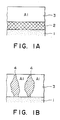
- Figs. 1A and 1B are schematic views for explaining the phenomenon of local crystallization of silicon.
- a polycrystalline silicon layer 2 is formed on an insulating substrate 1 such as of SiO2, and an aluminum layer 3 thicker than said polycrystalline silicon layer 2 is formed thereon.
- a coarse thin silicon film usable as the base of a coarse resistor film can be obtained by chemical elimination of aluminum alone. Therefore a coarse thin film can be obtained with satisfactory reproducibility, by selecting two parameters of the temperature of heat treatment and thickness of aluminum layer, without the conventional forming process.
- an electron emitting device can be formed even on a semiconductor device, since the coarse thin resistor film can be formed without the forming process on a silicon wafer or on an insulating layer.
- the coarse thin silicon film facilitates the formation of silicide or oxide of the material for reducing the work function, such as alkali metal, thereby easily achieving stable electron emission.
- the coarse thin silicon film allows easy adjustment of resistance through the control of impurity concentration in silicon.
- Fig. 2A is a schematic cross-sectional view of the electron emitting device embodying the present inveniton
- Fig. 2B is a magnified cross-sectional view of the resistor film thereof.
- a SiO2 layer 12 is formed by oxidation or chemical vapor deposition, and, in a desired position on said layer, there is formed a coarse thin resistor layer 17 by a process to be explained later. Subsequently formed are electrodes 18, 19 connected to the ends of the thin resistor film 17 and an electrode 20 on the rear side of the substrate 11.
- the coarse thin resistor film 17 is composed of a coarse thin silicon film 21 provided, at the surface thereof, with a CsSi3 layer 22 and a CsO layer 23, which serve to reduce the work function, thus increasing the quantity of electron emission. Also stable electron emission can be achieved since cesium is present in the states of silicide and oxide.
- electrons are efficiently and stably emitted by applying an AC (or DC) voltage across the electrodes 18, 19 and applying a voltage across the electrode 20 and the electrodes 18, 19 in such a manner that the latter assumes a higher potential.
- Figs. 3A to 3C are schematic views illustrating an embodiment of the process steps for producing the electron emitting device of the present invention.
- the SiO2 layer 12 is formed by oxidation or chemical vapor deposition on the silicon substrate 11. Then a polycrystalline silicon layer 13 is formed thereon, and further formed thereon is an aluminum layer 14 of a thickness larger than that of said polycrystalline silicon layer 13.
- the total thickness of the polycrystalline silicon layer 13 and of the aluminum layer 14 can be selected within a range from 200 ⁇ to 2 ⁇ m.
- the aluminum area 15 are selectively removed by etching, thereby leaving a coarse thin silicon layer 21 as shown in Fig. 3C.
- cesium is employed as the work function reducing material, but there can naturally be employed other alkali metals such as Rb or alkali earth metals.
- the electron emitting device of the foregoing embodiment and the producing process therefor allow to obtain a coarse thin silicon film through a simple process utilizing the local crystallization of silicon. Not requiring the conventional forming process, the coarse thin silicon film can be formed with a satisfactory reproducibility, by selecting two parameters of the temperature of heat treatment and thickness of aluminum layer.
- the electron emitting device can be formed easily on a semiconductor device and can therefore be integrated for example with a driving circuit. It is therefore possible to easily produce a compact electron emitting apparatus.
- the use of the coarse thin silicon film facilitates the formation of silicide and oxide of the work function reducing material such as alkali metal, thus improving and stabilizing the electron emission.
- the use of the coarse thin silicon film enables easy adjustment of resistance through the control of impurity concentration in silicon.
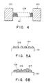
- Fig. 4 is a schematic plan view of the electron emitting device constituting another embodiment of the present invention.
- an insulating member 101 such as a glass plate, there are provided electrodes 102, 103 for current supply, between which formed is a coarse high resistance film 104 composed of fine particles.
- Fig. 5A is a schematic cross-sectional view of an example of the coarse high resistance film 104 in the present embodiment
- Fig. 5B is a schematic cross-sectional view showing another example of the coarse high resistance film 104 in the present embodiment.
- metal particles of a size of 0.1 to 10 ⁇ m are formed with a distance of 10 - 100 ⁇ on the insulating member 101 to constitute a coarse high resistance film 104 having discontinuous areas of regular distribution in the sense that the size and gap of the particles are relatively uniform.
- metal particles 106 of a size of 0.1 to 10 ⁇ m, having a surfacial oxide layer 107 of a thickness of several to several hundred Angstroms, are formed on the insulating member 101 to constitute a coarse high resistance film 104 having discontinuous areas of regular distribution, across said oxide layers 107.
- Fig. 6A is a schematic plan view of another embodiment of the present invention
- Fig. 6B is a cross-sectional view along a line I-I therein.
- a coarse high resistance film 108 is obtained by forming a metal film 109 by evaporation, and forming slits 110 in a grating pattern on said film 109 with a focused ion beam, a reactive ion beam or an electron beam, thereby forming regular notches.
- the slits 110 are 10 - 5000 ⁇ in width and 0.1 ⁇ 10 ⁇ m in pitch.
- the above-explained process provides a coarse high resistance film of a stable characteristic with reduced fluctuation. Besides said film can be easily formed even when it is integrated with another semiconductor device, as the current supply at a high temperature is unnecessary.
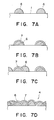
- Figs. 7A to 7D are schematic views showing process steps for producing the coarse high resistance film 104.
- metal particles of a size of 0.1 - 10 ⁇ m, composed of copper in this case, are deposited by ordinary evaporation on the insulating member 110 on which electrodes 102, 103 are formed in advance.
- the metal particles 106 can be formed in a fine particulate structure by setting the insulating member 101 at a relatively high temperature, and the particle size can be controlled by the rate and time of evaporation, and the temperature of substrate.
- the metal is not limited to Cu but can be Pb, Al or other metals.
- the metal particles 106 are oxidized or nitrogenated to obtain a thin oxide or nitride layer 107 of a thickness of several to several hundred Angstroms on the surface of said particles.
- metal particles 106 are again deposited by ordinary evaporation and are oxidized or nitrogenated.
- the above-explained evaporation and oxidization are repeated by a number of desired times to obtain, as shown in Fig. 7D, a coarse high resistance film 104 in which the metal particles 106 are separated by the oxide or nitride layer 107, thus having regular discontinuous areas.
- the electron emitting device of the foregoing embodiment is optimized in structure and has an improved electron emitting efficiency, as the discontinuities are regularly distributed in the coarse high resistance film. Also the regular formation of the film reduces the device-to-device fluctuation in case of mass production, and allows to obtain the electron emitting devices of uniform characteristic.
Landscapes
- Engineering & Computer Science (AREA)
- Manufacturing & Machinery (AREA)
- Cold Cathode And The Manufacture (AREA)
Priority Applications (1)
| Application Number | Priority Date | Filing Date | Title |
|---|---|---|---|
| EP93120390A EP0602663B1 (de) | 1986-07-04 | 1987-07-03 | Elektronen emittierende Vorrichtung |
Applications Claiming Priority (4)
| Application Number | Priority Date | Filing Date | Title |
|---|---|---|---|
| JP61156265A JPS6313227A (ja) | 1986-07-04 | 1986-07-04 | 電子放出素子およびその製造方法 |
| JP156265/86 | 1986-07-04 | ||
| JP210588/86 | 1986-09-09 | ||
| JP21058886 | 1986-09-09 |
Related Child Applications (2)
| Application Number | Title | Priority Date | Filing Date |
|---|---|---|---|
| EP93120390A Division EP0602663B1 (de) | 1986-07-04 | 1987-07-03 | Elektronen emittierende Vorrichtung |
| EP93120390.5 Division-Into | 1987-07-03 |
Publications (3)
| Publication Number | Publication Date |
|---|---|
| EP0251328A2 true EP0251328A2 (de) | 1988-01-07 |
| EP0251328A3 EP0251328A3 (en) | 1989-10-18 |
| EP0251328B1 EP0251328B1 (de) | 1995-01-04 |
Family
ID=26484066
Family Applications (2)
| Application Number | Title | Priority Date | Filing Date |
|---|---|---|---|
| EP93120390A Expired - Lifetime EP0602663B1 (de) | 1986-07-04 | 1987-07-03 | Elektronen emittierende Vorrichtung |
| EP87109607A Expired - Lifetime EP0251328B1 (de) | 1986-07-04 | 1987-07-03 | Elektronen-Emitter-Vorrichtung und ihr Herstellungsverfahren |
Family Applications Before (1)
| Application Number | Title | Priority Date | Filing Date |
|---|---|---|---|
| EP93120390A Expired - Lifetime EP0602663B1 (de) | 1986-07-04 | 1987-07-03 | Elektronen emittierende Vorrichtung |
Country Status (3)
| Country | Link |
|---|---|
| US (2) | US5559342A (de) |
| EP (2) | EP0602663B1 (de) |
| DE (2) | DE3752249T2 (de) |
Cited By (3)
| Publication number | Priority date | Publication date | Assignee | Title |
|---|---|---|---|---|
| EP0747921A3 (de) * | 1995-05-30 | 1996-12-18 | Canon Kabushiki Kaisha | Elektronenemittierende Vorrichtung, Elektronenquelle mit dieser elektronenemittierenden Vorrichtung, Bilderzeugungsgerät mit dieser Elektronenquelle und Herstellungsverfahren dieser elektronenemittierenden Vorrichtung |
| EP0757371A3 (de) * | 1995-08-03 | 1997-04-09 | Canon Kk | Elektronenemittierende Vorrichtung, Elektronenquelle und damit versehenes Bilderzeugungsgerät sowie Verfahren zu deren Herstellung |
| WO1999060598A1 (en) * | 1998-05-18 | 1999-11-25 | The Regents Of The University Of California | Low work function, stable compound clusters and generation process |
Families Citing this family (26)
| Publication number | Priority date | Publication date | Assignee | Title |
|---|---|---|---|---|
| USRE39633E1 (en) | 1987-07-15 | 2007-05-15 | Canon Kabushiki Kaisha | Display device with electron-emitting device with electron-emitting region insulated from electrodes |
| USRE40566E1 (en) | 1987-07-15 | 2008-11-11 | Canon Kabushiki Kaisha | Flat panel display including electron emitting device |
| USRE40062E1 (en) | 1987-07-15 | 2008-02-12 | Canon Kabushiki Kaisha | Display device with electron-emitting device with electron-emitting region insulated from electrodes |
| US5861227A (en) * | 1994-09-29 | 1999-01-19 | Canon Kabushiki Kaisha | Methods and manufacturing electron-emitting device, electron source, and image-forming apparatus |
| JP2946189B2 (ja) | 1994-10-17 | 1999-09-06 | キヤノン株式会社 | 電子源及び画像形成装置、並びにこれらの活性化方法 |
| JP3241251B2 (ja) * | 1994-12-16 | 2001-12-25 | キヤノン株式会社 | 電子放出素子の製造方法及び電子源基板の製造方法 |
| JP3299096B2 (ja) | 1995-01-13 | 2002-07-08 | キヤノン株式会社 | 電子源及び画像形成装置の製造方法、並びに電子源の活性化処理方法 |
| JP3315652B2 (ja) | 1998-09-07 | 2002-08-19 | キヤノン株式会社 | 電流出力回路 |
| GB9919737D0 (en) * | 1999-08-21 | 1999-10-20 | Printable Field Emitters Limit | Field emitters and devices |
| JP2001319567A (ja) * | 2000-02-28 | 2001-11-16 | Ricoh Co Ltd | 電子源基板および該電子源基板を用いた画像表示装置 |
| JP3610325B2 (ja) * | 2000-09-01 | 2005-01-12 | キヤノン株式会社 | 電子放出素子、電子源及び画像形成装置の製造方法 |
| US6781146B2 (en) * | 2001-04-30 | 2004-08-24 | Hewlett-Packard Development Company, L.P. | Annealed tunneling emitter |
| US6911768B2 (en) | 2001-04-30 | 2005-06-28 | Hewlett-Packard Development Company, L.P. | Tunneling emitter with nanohole openings |
| US6753544B2 (en) | 2001-04-30 | 2004-06-22 | Hewlett-Packard Development Company, L.P. | Silicon-based dielectric tunneling emitter |
| US6882100B2 (en) * | 2001-04-30 | 2005-04-19 | Hewlett-Packard Development Company, L.P. | Dielectric light device |
| US6558968B1 (en) | 2001-10-31 | 2003-05-06 | Hewlett-Packard Development Company | Method of making an emitter with variable density photoresist layer |
| US6703252B2 (en) * | 2002-01-31 | 2004-03-09 | Hewlett-Packard Development Company, L.P. | Method of manufacturing an emitter |
| US6835947B2 (en) * | 2002-01-31 | 2004-12-28 | Hewlett-Packard Development Company, L.P. | Emitter and method of making |
| US6852554B2 (en) | 2002-02-27 | 2005-02-08 | Hewlett-Packard Development Company, L.P. | Emission layer formed by rapid thermal formation process |
| US6787792B2 (en) | 2002-04-18 | 2004-09-07 | Hewlett-Packard Development Company, L.P. | Emitter with filled zeolite emission layer |
| US7170223B2 (en) | 2002-07-17 | 2007-01-30 | Hewlett-Packard Development Company, L.P. | Emitter with dielectric layer having implanted conducting centers |
| WO2008039461A2 (en) * | 2006-09-27 | 2008-04-03 | Thinsilicon Corp. | Back contact device for photovoltaic cells and method of manufacturing a back contact |
| WO2008150769A2 (en) * | 2007-05-31 | 2008-12-11 | Thinsilicon Corporation | Photovoltaic device and method of manufacturing photovoltaic devices |
| KR101319674B1 (ko) * | 2009-05-06 | 2013-10-17 | 씬실리콘 코포레이션 | 광기전 전지 및 반도체층 적층체에서의 광 포획성 향상 방법 |
| US20110114156A1 (en) * | 2009-06-10 | 2011-05-19 | Thinsilicon Corporation | Photovoltaic modules having a built-in bypass diode and methods for manufacturing photovoltaic modules having a built-in bypass diode |
| WO2010144459A2 (en) * | 2009-06-10 | 2010-12-16 | Thinsilicon Corporation | Photovoltaic modules and methods for manufacturing photovoltaic modules having tandem semiconductor layer stacks |
Family Cites Families (9)
| Publication number | Priority date | Publication date | Assignee | Title |
|---|---|---|---|---|
| US3581151A (en) * | 1968-09-16 | 1971-05-25 | Bell Telephone Labor Inc | Cold cathode structure comprising semiconductor whisker elements |
| US3611077A (en) * | 1969-02-26 | 1971-10-05 | Us Navy | Thin film room-temperature electron emitter |
| US3814968A (en) * | 1972-02-11 | 1974-06-04 | Lucas Industries Ltd | Solid state radiation sensitive field electron emitter and methods of fabrication thereof |
| US3806372A (en) * | 1972-06-02 | 1974-04-23 | Rca Corp | Method for making a negative effective-electron-affinity silicon electron emitter |
| US3990914A (en) * | 1974-09-03 | 1976-11-09 | Sensor Technology, Inc. | Tubular solar cell |
| US3936329A (en) * | 1975-02-03 | 1976-02-03 | Texas Instruments Incorporated | Integral honeycomb-like support of very thin single crystal slices |
| NL184589C (nl) * | 1979-07-13 | 1989-09-01 | Philips Nv | Halfgeleiderinrichting voor het opwekken van een elektronenbundel en werkwijze voor het vervaardigen van een dergelijke halfgeleiderinrichting. |
| US4683399A (en) * | 1981-06-29 | 1987-07-28 | Rockwell International Corporation | Silicon vacuum electron devices |
| JPS60221926A (ja) * | 1984-04-19 | 1985-11-06 | Sony Corp | 放電表示装置の製造方法 |
-
1987
- 1987-07-03 EP EP93120390A patent/EP0602663B1/de not_active Expired - Lifetime
- 1987-07-03 DE DE3752249T patent/DE3752249T2/de not_active Expired - Lifetime
- 1987-07-03 EP EP87109607A patent/EP0251328B1/de not_active Expired - Lifetime
- 1987-07-03 DE DE3750936T patent/DE3750936T2/de not_active Expired - Lifetime
-
1995
- 1995-04-06 US US08/418,091 patent/US5559342A/en not_active Expired - Fee Related
- 1995-06-07 US US08/472,111 patent/US5627111A/en not_active Expired - Fee Related
Cited By (6)
| Publication number | Priority date | Publication date | Assignee | Title |
|---|---|---|---|---|
| EP0747921A3 (de) * | 1995-05-30 | 1996-12-18 | Canon Kabushiki Kaisha | Elektronenemittierende Vorrichtung, Elektronenquelle mit dieser elektronenemittierenden Vorrichtung, Bilderzeugungsgerät mit dieser Elektronenquelle und Herstellungsverfahren dieser elektronenemittierenden Vorrichtung |
| US5939824A (en) * | 1995-05-30 | 1999-08-17 | Canon Kabushiki Kaisha | Electron emitting device having a conductive thin film formed of at least two metal elements of difference ionic characteristics |
| CN1090379C (zh) * | 1995-05-30 | 2002-09-04 | 佳能株式会社 | 电子发射器件及制法,具有该器件的电子源及成象装置 |
| EP0757371A3 (de) * | 1995-08-03 | 1997-04-09 | Canon Kk | Elektronenemittierende Vorrichtung, Elektronenquelle und damit versehenes Bilderzeugungsgerät sowie Verfahren zu deren Herstellung |
| US6184610B1 (en) * | 1995-08-03 | 2001-02-06 | Canon Kabushiki Kaisha | Electron-emitting device, electron source and image-forming apparatus |
| WO1999060598A1 (en) * | 1998-05-18 | 1999-11-25 | The Regents Of The University Of California | Low work function, stable compound clusters and generation process |
Also Published As
| Publication number | Publication date |
|---|---|
| DE3752249D1 (de) | 1999-03-04 |
| EP0251328B1 (de) | 1995-01-04 |
| DE3750936T2 (de) | 1995-05-18 |
| EP0602663A1 (de) | 1994-06-22 |
| DE3750936D1 (de) | 1995-02-16 |
| EP0602663B1 (de) | 1999-01-20 |
| DE3752249T2 (de) | 1999-07-08 |
| US5559342A (en) | 1996-09-24 |
| US5627111A (en) | 1997-05-06 |
| EP0251328A3 (en) | 1989-10-18 |
Similar Documents
| Publication | Publication Date | Title |
|---|---|---|
| EP0251328A2 (de) | Elektronen-Emitter-Vorrichtung und ihr Herstellungsverfahren | |
| US5176557A (en) | Electron emission element and method of manufacturing the same | |
| US5576051A (en) | Multiple electron emission device | |
| JP2630988B2 (ja) | 電子線発生装置 | |
| US5201681A (en) | Method of emitting electrons | |
| US5188977A (en) | Method for manufacturing an electrically conductive tip composed of a doped semiconductor material | |
| US5382867A (en) | Field-emission type electronic device | |
| US5661362A (en) | Flat panel display including electron emitting device | |
| US3998678A (en) | Method of manufacturing thin-film field-emission electron source | |
| JP2715304B2 (ja) | Mim形電子放出素子 | |
| US5394006A (en) | Narrow gate opening manufacturing of gated fluid emitters | |
| EP0713241B1 (de) | Ein Elektronenemissionselement enthaltende Anzeigevorrichtung | |
| EP0708472A1 (de) | Herstellung eines Mikro-Elektronenemitters | |
| US5391956A (en) | Electron emitting device, method for producing the same and display apparatus and electron beam drawing apparatus utilizing the same | |
| JPH09219144A (ja) | 電界放出カソードとその製造方法 | |
| US5327050A (en) | Electron emitting device and process for producing the same | |
| KR20030056572A (ko) | 전계 방출 소자용 캐소드 | |
| JP2003162956A (ja) | Mis/mim電子放出素子 | |
| JP2809078B2 (ja) | 電界放出冷陰極およびその製造方法 | |
| JPH07114104B2 (ja) | 電子放出素子及びその製造方法 | |
| JPH09129123A (ja) | 電子放出素子及びその製造方法 | |
| JPH0797473B2 (ja) | 電子放出素子 | |
| JP3638264B2 (ja) | 冷陰極装置の作製方法及び冷陰極装置並びにそれを用いた表示装置 | |
| JP3622406B2 (ja) | 冷電子放出素子及びその製造方法 | |
| JP2612569B2 (ja) | 電子放出素子 |
Legal Events
| Date | Code | Title | Description |
|---|---|---|---|
| PUAI | Public reference made under article 153(3) epc to a published international application that has entered the european phase |
Free format text: ORIGINAL CODE: 0009012 |
|
| AK | Designated contracting states |
Kind code of ref document: A2 Designated state(s): DE FR GB |
|
| PUAL | Search report despatched |
Free format text: ORIGINAL CODE: 0009013 |
|
| AK | Designated contracting states |
Kind code of ref document: A3 Designated state(s): DE FR GB |
|
| 17P | Request for examination filed |
Effective date: 19900305 |
|
| 17Q | First examination report despatched |
Effective date: 19910327 |
|
| GRAA | (expected) grant |
Free format text: ORIGINAL CODE: 0009210 |
|
| AK | Designated contracting states |
Kind code of ref document: B1 Designated state(s): DE FR GB |
|
| REF | Corresponds to: |
Ref document number: 3750936 Country of ref document: DE Date of ref document: 19950216 |
|
| ET | Fr: translation filed | ||
| PLBE | No opposition filed within time limit |
Free format text: ORIGINAL CODE: 0009261 |
|
| STAA | Information on the status of an ep patent application or granted ep patent |
Free format text: STATUS: NO OPPOSITION FILED WITHIN TIME LIMIT |
|
| 26N | No opposition filed | ||
| REG | Reference to a national code |
Ref country code: GB Ref legal event code: IF02 |
|
| PGFP | Annual fee paid to national office [announced via postgrant information from national office to epo] |
Ref country code: GB Payment date: 20060628 Year of fee payment: 20 |
|
| PGFP | Annual fee paid to national office [announced via postgrant information from national office to epo] |
Ref country code: DE Payment date: 20060629 Year of fee payment: 20 |
|
| PGFP | Annual fee paid to national office [announced via postgrant information from national office to epo] |
Ref country code: FR Payment date: 20060719 Year of fee payment: 20 |
|
| REG | Reference to a national code |
Ref country code: GB Ref legal event code: PE20 |
|
| PG25 | Lapsed in a contracting state [announced via postgrant information from national office to epo] |
Ref country code: GB Free format text: LAPSE BECAUSE OF EXPIRATION OF PROTECTION Effective date: 20070702 |