EP0251521A2 - Système de déflexion de faisceau avec fourniture de puissance selon les besoins pour affichages à tubes à rayons cathodiques à deux modes - Google Patents
Système de déflexion de faisceau avec fourniture de puissance selon les besoins pour affichages à tubes à rayons cathodiques à deux modes Download PDFInfo
- Publication number
- EP0251521A2 EP0251521A2 EP87305052A EP87305052A EP0251521A2 EP 0251521 A2 EP0251521 A2 EP 0251521A2 EP 87305052 A EP87305052 A EP 87305052A EP 87305052 A EP87305052 A EP 87305052A EP 0251521 A2 EP0251521 A2 EP 0251521A2
- Authority
- EP
- European Patent Office
- Prior art keywords
- deflection
- current
- coupled
- voltage
- transistor
- Prior art date
- Legal status (The legal status is an assumption and is not a legal conclusion. Google has not performed a legal analysis and makes no representation as to the accuracy of the status listed.)
- Granted
Links
- 230000009977 dual effect Effects 0.000 title 1
- 230000000737 periodic effect Effects 0.000 claims abstract description 4
- 238000010894 electron beam technology Methods 0.000 claims description 8
- 238000012544 monitoring process Methods 0.000 abstract 1
- 230000001965 increasing effect Effects 0.000 description 6
- 238000010586 diagram Methods 0.000 description 5
- 238000005070 sampling Methods 0.000 description 5
- 230000003247 decreasing effect Effects 0.000 description 4
- 230000000694 effects Effects 0.000 description 3
- 230000001939 inductive effect Effects 0.000 description 3
- 239000004065 semiconductor Substances 0.000 description 2
- 230000003213 activating effect Effects 0.000 description 1
- 230000001419 dependent effect Effects 0.000 description 1
- 230000003292 diminished effect Effects 0.000 description 1
- 238000002955 isolation Methods 0.000 description 1
- 239000013642 negative control Substances 0.000 description 1
- 239000013641 positive control Substances 0.000 description 1
- 230000035945 sensitivity Effects 0.000 description 1
Images


Classifications
-
- G—PHYSICS
- G09—EDUCATION; CRYPTOGRAPHY; DISPLAY; ADVERTISING; SEALS
- G09G—ARRANGEMENTS OR CIRCUITS FOR CONTROL OF INDICATING DEVICES USING STATIC MEANS TO PRESENT VARIABLE INFORMATION
- G09G1/00—Control arrangements or circuits, of interest only in connection with cathode-ray tube indicators; General aspects or details, e.g. selection emphasis on particular characters, dashed line or dotted line generation; Preprocessing of data
- G09G1/04—Deflection circuits ; Constructional details not otherwise provided for
Definitions
- the invention relates generally to electromagnetically deflected beam display systems and more particularly to power supply control circuits for providing linear operation and high efficiency in random stroke and periodic raster display modes and during slew of a cathode ray tube electron beam.
- the power efficiency of deflection systems that display both raster and stroke writing is relatively low due to the inductive deflection yoke and the high driving voltages required for magnetic deflection to assure adequate writing speed.
- Sophisticated airborne navigation displays with increased display area and information content require a significant increase in power consumption, while space and available power is limited. Since the deflection yoke driving circuit consumes a significant portion of the total display power, the power efficiency of the deflection system may be greatly enhanced if the required driving voltages can be reduced.
- the present invention describes a system for optimising power conservation during the raster and stroke displays while permitting increased slewing speed.
- the invention is controlled by internal signals developed in the yoke driver amplifier without the need for external control signals. Since the internal switch control signals do not discriminate between stroke and raster operation, stroke writing efficiency is optimised even at high slewing speeds. Moreover, minimum power dissipation is also obtained during slewing conditions by varying the applied yoke driver voltages to that required to obtain linear operation.
- the present invention is defined in the appended claims and provides a deflection system for a cathode ray tube employing a magnetic deflection coil to position the beam of a cathode ray tube along its face comprises a differential amplifier, a feedback element, a deflection amplifier, a plurality of voltage sources, a preamplifier, and a plurality of switches.
- the differential amplifier responds to beam positional signals and to a feedback signal representative of the current through the deflection coil.
- the error signal thereby developed is coupled to drive the preamplifier, which in turn causes the deflection amplifer to provide a current proportional to the input signal to the deflection coil.
- the switches are connected to the voltage sources to selectively and independently supply the deflection amplifier with sufficient current to maintain linear operation in raster, stroke, and slew modes of operation while minimising power consumption.
- Control signals for activating the switches are derived by sensing the voltage developed across the deflection coil and the current flowing therethrough.
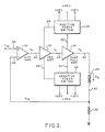
- a power on demand electron beam magnetic deflection system operable to provide linear deflection in the stroke mode for random deflection of the beam and while slewing the beam, and in the raster mode for periodic deflection of the beam, includes a differential amplifier lO, a preamplifier l2, a push-pull amplifier stage l4, a deflection yoke 20 mounted on a cathode ray tube (CRT) (not shown), and a yoke current sampling resistor 22.
- CTR cathode ray tube
- a positive power switch l6 coupled to receive current from a plurality of power supplies +l5V, +45V, and -l5V receives control signals from preamplifier l2 on line 24 and energises push-pull amplifier l4 on line 28.
- a negative power switch l8 receives current from -l5V, -45V, and +l5V power supplies and control signals from preamplifier l2 via line 26, and provides current to push-pull amplifier l4 on line 30.
- An input signal V IN representative of the desired beam deflection, which may be in stroke mode, raster mode, or during slewing of the beam, is applied on line 36 to the non-inverting input of differential amplifier lO.
- a feedback signal V FB derived by sensing a voltage drop across resistor 22 proportional to yoke current I O , is provided on line 38 to the inverting input of differential amplifier lO.
- the two signals are algebraically subtracted and amplified in differential amplifier lO to provide an error signal V e on line 40 which is coupled to the input of preamplifier l2.
- Preamplifier l2 provides an amplified voltage V I for driving push-pull amplifier l4.
- Amplifier l4 operates in a conventional manner to provide an output signal V O on line 42 for driving a magnetising current I O through deflection yoke 20.
- the current I O also flows through series connected line 32 to sampling resistor 22 to develop a feedback signal V FB .
- the signal V FB is proportional in magnitude and polarity to the current I O .
- a deflection signal V IN is applied to differential amplifier lO to develop an output signal V e .
- Signal V e is amplified by preamplifier l2 to provide a driving signal V I to push-pull amplifier l4.
- Amplifier l4 provides an output signal V O to energise deflection yoke 2O.
- the current I O flowing in yoke 2O is sampled in series resistor 22 to develop a feedback signal V FB which is proportional to the current I O .
- Differential amplifier lO algebraically combines V IN and V FB to develop resultant signal V e . This signal drives the preamplifier l2 and push-pull amplifier l4 in closed loop fashion so that the current waveform I O replicates the deflection signal V IN .
- power switches l6 and l8 are individually energised to select one of a plurality of power supplies in accordance with substantially the minimum supply voltage required to assure linear operation.
- a control signal on line 24 from preamplifer l2 energises power switch l6 is responsive to the deflection command V IN on line 36 and to the feedback signal V FB on line 38.
- the magnitude of signal V O is sensed and communicated to switch l6 through amplifier l4. The combination of these signals determines which of the supplies coupled to switch l6 will be made available on line 28 to push-pull amplifier l4.
- negative power switch l8 which energises yoke 20 when negative deflection current is commanded, follows in a similar manner to energise the lower section of push-pull amplifier l4 in response to control signals on lines 26 and 30.
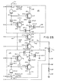
- FIG. 2 illustrates a schematic circuit diagram of a preferred embodiment of the invention. Not shown are conventional circuit elements used to enhance the frequency response, increase transistor current gain, and stabilise the system.
- Input stage lO comprises a conventional differential amplifier coupled to receive the beam deflection signal V IN on line 36 at one input and a feedback signal V FB developed across resistor 22 and coupled at node 56 to a second input on line 38 to sample the current passing through deflection yoke 20.
- the output of amplifier lO is an error voltage V e which is applied on line 40 to current amplifier ll of preamplifier l2.
- Current amplifier ll draws current from a +l5V supply through transistor Ql and from the +45V supply through transistors Q2, Q7 and Q8.
- Amplifier ll draws current I1 at pins l and 2 from emitter l5a of transistor Ql. Amplifier ll is further energised at pins 7 and 6 from a-l5V supply through transistor Q9 and from a -45V supply through transistors QlO, Qll, and Ql2. The output 4 of amplifier ll is coupled to load resistor l3, which is connected to ground at reference numeral 9. Coupled between the collectors of transistors Q2 and QlO are series connected diodes CR3-CR8 which provide predetermined bias voltages V B , V C , V D and V E .
- Current amplifier ll is a unity gain buffer, such as type LHOOO2 as manufactured by National Semiconductor Corp., Santa Clara, CA.
- the cathode of diode CR3 is coupled to the anode of diode CR4.
- the cathode of diode CR4 connects at node 47 to base 57b of transistor Q5 and to the anode of diode CR5.
- the cathode of diode CR5 is coupled to the anode of diode CR6 and the cathode thereof connected at node 49 to the anode of diode CR7 and the base 59b of transistor Q6.
- Diode CR7 has its cathode connected to the anode of diode CR8.
- a positive voltage source of +l5V at terminal 56 is applied to the base l5c of transistor Ql.
- Transistor Q1 draws current I3 from transistors Q2 and Q8.
- Transistors Q2, Q7, and Q8 are connected in a PNP Wilson Constant Current Source configuration such as is commonly employed in operational amplifier microcircuits.
- the base l7c of transistor Q2 is coupled to the collector 2lb of transistor Q8 and the collector l5b of transistor Ql at node 23.
- Emitter l7a of transistor Q2 and collector l9b of transistor Q7 are coupled at node 25 to the base l9c of transistor Q7 and base 2lc of transistor Q8.
- Emitters l9a and 2la of transistors Q7 and Q8, respectively, are connected in common at node 27 to a positive high voltage supply at terminal 70, typically +45V.
- Collector l7b of transistor Q2 is coupled to the anode of diode CR3 and the cathode of diode CR2 at node 24.
- Pins 6 and 7 of amplifier ll are coupled to supply current I2 to emitter 3la of NPN transistor Q9.
- the base 3lb of transistor Q9 is coupled to a -l5V power source.
- Transistors QlO, Qll, and Ql2 are connected in an NPN Wilson Current Source configuration.
- the collector 3lc of transistor Q9 is coupled to base 33b of transistor QlO and collector 37c of transistor Qll at node 35.
- Emitter 33a of transistor QlO is coupled to collector 4lc and base 4lb of transistor Ql2 and also coupled to base 37b of transistor Qll at node 39.
- Emitters 37a and 4la of transistors Qll and Ql2 are coupled at node 43 to a -45V power supply.
- the collector 33c of transistor QlO is coupled at node 26 to the base 6lb of transistor Q4, the cathode of diode CR8, and the anode of diode CR9 of the negative power switch l8.
- the positive power switch l6 is comprised of transistors Q3 and Ql3 and diodes CRl, CR2, CRll, CRl3, and CRl4, and coupled to +l5V, -l5V, and +45V power supplies.
- the +45V power supply at terminal 70 is coupled at node 27 to the anode of a constant current unidirectional conducting element CRl such as type IN53l4, as manufactured by Motorola Semiconductor Corp.
- the cathode of diode CRl connects at node 45 to the base 53b of transistor Ql3 and the anode of diode CR2.
- the cathode of diode CR2 is coupled at node 24 to the anode of diode CR3, the collector l7b of transistor Q2 and to the base 55b of transistor Q3.
- the collector 53c of transistor Ql3 is connected to a +l5V voltage source at terminal 68.
- a diode CRl3 has its anode coupled to the emitter 53a of transistor Ql3 and its base coupled to node 65.
- a diode CRl4 has its anode coupled to a -l5V power source at termianl 66 and the cathode coupled to nodes 65 and 67.
- Emitter 55a of transistor Q3 is coupled to the anode of diode CRll.
- Node 67 is coupled to the cathode of diode CRll and to the collector 57c of transistor Q5.
- a +45V supply at terminal 7l is coupled to collector 55c of transistor Q3.
- negative power switch l8 is comprised of transistors Q4 and Ql4, diodes CR9, CRlO, CRl2, CRl5, and CRl6, and coupled to power sources supplying +l5V, -l5V, and -45V.
- the cathode of diode CR9 connects at node 57 to the base 63b of transistor Ql4 and the anode of a constant current unidirectional conducting element CRlO.
- the cathode of element CRlO connects at node 43 to the -45V power source at terminal 76.
- Emitter 63a of transistor Ql4 is connected to the cathode of diode CRl5 and collector 63c to a -l5V power source at terminal 74.
- Collector 59a of transistor Q6 connects to the anodes of diodes CRl2, CRl5 and CRl6 at node 54.
- the cathode of diode CRl2 is coupled to emitter 6lc of transistor Q4.
- Collector 6lA of transistor Q4 is connected to a -45V power source at terminal 69.
- the cathode of diode CRl6 is connected to a +l5V power source at terminal 72.
- Node 5l is connected to base 63b of transistor Ql4.
- Push-pull amplifier l4 is comprised of diodes CR5 and CR6 and cascaded transistors Q5 and Q6 whose common emitter junction at node 52 is connected via lead 42 to energise deflection coil 20.
- Node 47 of the diode chain connects via lead 46 to the base 57b of transistor Q5.
- Emitter 57a of transistor Q5 connects via node 52 to emitter 59c of transistor Q6 and to one end of deflection yoke 20.
- Node 49 of the diode chain connects to base 59b of transistor Q6.
- the second end of deflection coil 20 is connected at node 56 to sampling resistor 22 and by line 38 to input the negative of differential amplifier lO. Sampling resistor 22 is terminated to ground at reference numeral 58.
- a signal V IN applied to differential amplifier lO will result in a current I O proportional thereto in yoke 20.
- a positive-going signal applied to lead 36 will result in a positive yoke current
- a negative-going signal applied to lead 36 will result in a negative current in yoke 20.
- a positive error voltage V will be applied to current amplifier ll.
- Power is drawn in the direction shown by arrow I1 from the emitter of transistor Q1 to pins l and 2 of current amplifier ll.
- Transistor Q1 acts to buffer current amplifier ll from the high voltage power sources.
- Collector current I3 of transistor Q1 is substantially equal in value to emitter current I1.
- Transistors Q7 and Q8 are a matched pair configured as a Wilson current source and provide a current output I5 at transistor Q2 which is equal in magnitude to the current I3 but oppositely polarised.
- Amplifier ll also supplies idle current at pins 6 and 7 to buffer transistor Q9.
- the output current I4 at the collector of Q9 is equal to the input current I2 from pins 6 and 7 of amplifier ll flowing to emitter 3la of transistor Q9.
- a current I6 at the collector 33c of transistor Q10 is drawn through the diode chain CR2-CR9 and is equal in magnitude to the idle current I4.
- preamplifier l2 provides bias voltages V B , V C , V D and V E , determined by the predetermined diode voltage drops across CR3-CR8. In operation, with power supplies of ⁇ 45 V, the output voltage V1 will range over approximately ⁇ 4l.5 V.
- the function of power control switches l6 and l8 is to supply the collectors of the output transistors Q5 and Q6 with the lowest supply voltage that will permit maintaining linear operation.
- one of the +45 V, +l5 V, or -l5 V supplies is selected by the positive power control circuitry and one of the -45 V, -l5 V, or +l5 V supplies is selected to supply negative output current to the collector of transistor Q6.
- the sequential operation of the power control switches may be readily understood by consideration of an example. Since the amplifier l4 is driving an inductive load 20, the following polarity conditions for amplifier output voltage V O and yoke current I O will exist: Note that unlike a resistive load, a negative output voltage must be developed for positive output current and vice versa under some conditions of operation. All positive output current I O is supplied by the positive power switch l6, and all negative output current is provided by the negative power switch l8.
- the power control circuitry will select the lowest supply voltage as a function of the required electron beam deflection rate.
- the actual magnitude of the power supplies which are selected by the power switches is a function of the deflection rate of the input signal V IN .
- a sine wave input signal may be selected for V IN , which will exercise a deflection amplifier of the type shown in Figure 2 over a writing rate up to approximately 236 in/sec on a 6 ⁇ ⁇ 6 ⁇ CRT face with 48° on-axis deflection angle.
- Figure 3 shows the output voltage waveform V O required to obtain an output current I O that is a replica of V IN .
- a sine wave input with a period of 8O ⁇ S is chosen for ease of analysis and to illustrate exercising both positive and negative control circuitry. It is assumed that a peak voltage of l V is applied. With sine wave input, the rate of change of current through the yoke ranges from O A/sec to 230 KA/sec.
- V IN sin (7.85 ⁇ l04t) (l)
- V O L + I O (R Y + R S ) (2)
- L inductance of yoke (l80 ⁇ h)
- dI O /dt rate of change of output current with respect to time
- I O yoke current (amp)
- R Y yoke resistance (0.6 ohm)
- R S sample resistor (0.34 ohm)
- V O (l80 ⁇ h) (35 Kin/sec) (3.lA/3 in) + I O (0.6 + 0.34 ohms) (6)
- V O 6.5l + 0.94 I O
- V O -6.5l + 0.94 I O
- V O 6.5l + 34 ⁇ l03t (l0)
- V O -6.5l - 34 x l03t (ll)
- the required supply voltage will be a function of the desired output voltage and the polarity of output current, which in turn depends on the yoke inductances and rate of deflection of the electron beam.
- Figure 3 shows a family of waveforms corresponding to a sinusoidal deflection voltage V IN .
- Curve V IN shows a sine wave with amplitude 2 V peak-to-peak.
- the time base is divided into six intervals lOO, lO2, lO4, lO6, lO8 and llO, each interval corresponding to the utilisation of a particular power supply. While six supplies have been chosen for illustrative purposes, this is by way of example only and in principle the number of supplies may be extended or diminished.
- V IN Corresponding to the deflection voltage curve V IN is the curve V O of the output voltage across deflection coil 2O. Since the coil is primarily inductive, the output voltage is shifted in phase by 90° in relation to the current I O . As an example, for the desired deflection on the CRT, a peak-to-peak amplitude of 93 V is required.
- the current waveform I O is in phase with the deflection voltage V IN by virtue of the feedback circuitry which forces the current waveform to be identical to the deflection voltage.
- the yoke current is scaled for a peak-to-peak value of 5.88A, which corresponds to a peak current of 2.94 A. Table 2 identifies the power supply voltage applied for each of the six intervals.
- Positive power switch l6 selects substantially the lowest supply voltage required to provide the desired output voltage V O .
- the output voltage V O ranges between +4l.5 and +l3.4 V.
- Transistor Q3 and diode CRll are biased into conduction while transistor Q13 and diode CRl3 are not conducting.
- Diode CRl4 is back biased and not conducting.
- Diode CR2 is back biased and not conducting.
- transistor Q3 and diode CRll conduct the output current from the +45 V supply at terminal 7l while the current paths from the +l5 V and -l5 V supplies are interrupted.
- Diode CRl essentially provides a constant current source and isolation of loading effects on the +45V supply.
- interval lO2 of Figure 3 The output voltage V O is seen to range between +l3.4 V and -l7.l V. Over this range, the voltage at node 65 will vary between -l5.7 V and +l4.l V. Diodes CRll and CRl4 will be biased for nonconduction over substantially the entire range. The voltage at node 45 varies from -l4.3V to +l5.5V, while at node 65 it varies between -l5.7 V and +l4.l V, so that transistor Q13 is biased for conduction. Diode CRl3 is forwarded biased so that the output current I O is supplied by the +l5 V supply at terminal 68.
- transistor Q5 The voltage at collector 57c of transistor Q5 will be between 0.7 to l.4 V above the output voltage V O and therefore transistor Q5 is always kept out of saturation.
- transistor Q3 and diode CRll during interval lO2 the voltage applied between nodes 24 and 67 is insufficient to bias the components to conductivity. Therefore, transistor Q3 and diode CRll will be nonconducting for output voltage V O ranging from -l7.l to +l3.4 V.
- the voltage difference between nodes 65 and 24 will range between -23.7 V to 0.7 V. Since this voltage must be at least l.4 V to forward bias diode CRll and transistor Q3 transistor Q3 is turned off for V O ranging between -4l.5 V to -l7.l V. Similarly, by counting diode drops for diodes CR2, CR3, CR4 and transistor Q5 it may be shown that the voltage difference between nodes 45 and 65 will range from -23 V to +l.4 V.
- transistor Q13 will be turned on when the voltage difference applied between the base 53b of transistor Q13 and the cathode of diode CR13 equals l.4 V, and thus will be turned off for values of V O less than -l7.l V.
- diode CRl4 conducts output current I O from the -l5 V supply at terminal 66 while diodes CRll and CRl3 are back biased and therefore not conducting current. Hence, the +45V and +l5V supplies are disconnected.
- V IN represents a triangular waveform with a peak value of l V.
- the corresponding deflection yoke current I O is also a triangular waveform of peak amplitude 2.94 A whose magnitude has been determined as described above. It may be seen that the voltage waveform V O describes a ramp increasing from 33.48 V to 39.3 V and decreasing from -33.48 V to -39.3 V.
- the intervals ll2, ll4, ll6, ll8 of Figure 5 designate time intervals corresponding to operation of the power switching circuitry.
- V IN is O V
- I O is O A
- V O is 36.4 V.
- the positive voltage V IN applied to amplifier lO results in a positive voltage V1 at the cathode of diode CR5.
- Bias V H l5.5V applied to the base 53b of transistor Q13 and 37.l V applied to the cathode of CR13 through diode CRll and transistor Q3, results in reverse biasing transistor Q13 and diode CRl3 by a value of -2l.6 V.
- the state of the positive power switching circuitry changes as follows: transistor Q3 and diode CRll are turned off because of the high negative bias appearing at node 24 coupled from the output voltage V O , allowing for the diode voltage drops in CR3, CR4 and Q5; the voltage V B at the base 55b of transistor Q3 is approximately -3l.4 V. Since diode CRl4 clamps V F to -l5.7 V, and since voltage V B and base 55b of transistor Q3 is -3l.4 V, diode CRll and transistor Q3 are back biased.
- Transistor Q13 and diode CRl3 are back biased because the voltage at node 45 and base 53b of transistor Q13 is -30.7 V, while the voltage at node 65 is -l5.7 V. Since diode CRl4 is biased for conduction, the output current I O is supplied from the -l5 V power supply terminal 66 and controlled by transistor Q5. These conductive states continue through interval ll4.
- the output voltage V O is continuing to decrease while V IN reaches a value of O V and I O has a value of OA.
- the output current I O changes in polarity from positive to negative. Therefore, transistor Q5 and diode CRl4 no longer conduct current and the output current is provided through transistors Q4 and Q6 and diode CRl2 from the -45 V supply at terminal 69.
- Diode CRl6 is reverse biased by the negative voltage V G applied at anode junction 54, which has a value of approximately -37.l V, and the +l5 V supply at the cathode.
- the positive voltage of 33.48 V developed across yoke 20 results in biasing diode CRl6 to be conductive and supplies current I O from the +l5 V supply at terminal 72 through transistor Q6.
- Transistor Q4 and diode CRl2 are reverse biased by the positive voltage V E - V G applied to node 26 with respect to node 54, so that the -45V supply is disconnected.
- Transistor Q14 and diode CRl5 remain nonconducting because of the positive bias V I -V G applied between nodes 5l and 54. Therefore no current is provided by the -l5 V supply at terminal 74.
- the foregoing conditions continue through interval ll8. At the end of interval ll8, the output current I O increases to positive polarity.
- transistor Q6 and diode CRl6 stop conducting current while transistors Q3 and Q5 and diode CRll are biased for positive conduction.
- transistors Q13 and Q14 remain off for the entire cycle and current does not flow through diodes CRl3 and CRl5. It may be seen from Table 2 that since the output voltage V O is not required to develop values in the range of -l7.l V to +l3.4 V for positive I O and +l7.l V to -l3.4 V for negative I O the plus and minus l5 V power supplies are not required and transistors Q13 and Q14 are not exercised.
- transistors Q13 and Q14 and the ⁇ l5 V power supplies are adequate to supply the current throughout the cycle and therefore transistors Q3 and Q4 and diodes CRll, CRl2, CRl4 and CRl6 remain nonconducting.
- the writing speed is increased to, for example, l80 Kin/sec, then the ⁇ 45 V power supplies will be required.
Landscapes
- Engineering & Computer Science (AREA)
- Radar, Positioning & Navigation (AREA)
- Remote Sensing (AREA)
- Physics & Mathematics (AREA)
- Computer Hardware Design (AREA)
- General Physics & Mathematics (AREA)
- Theoretical Computer Science (AREA)
- Details Of Television Scanning (AREA)
- Video Image Reproduction Devices For Color Tv Systems (AREA)
- Amplifiers (AREA)
- Cathode-Ray Tubes And Fluorescent Screens For Display (AREA)
- Devices For Indicating Variable Information By Combining Individual Elements (AREA)
- Vessels, Lead-In Wires, Accessory Apparatuses For Cathode-Ray Tubes (AREA)
Applications Claiming Priority (2)
| Application Number | Priority Date | Filing Date | Title |
|---|---|---|---|
| US06/879,730 US4712047A (en) | 1986-06-27 | 1986-06-27 | Power on demand beam deflection system for dual mode CRT displays |
| US879730 | 1986-06-27 |
Publications (3)
| Publication Number | Publication Date |
|---|---|
| EP0251521A2 true EP0251521A2 (fr) | 1988-01-07 |
| EP0251521A3 EP0251521A3 (en) | 1990-08-29 |
| EP0251521B1 EP0251521B1 (fr) | 1994-01-05 |
Family
ID=25374773
Family Applications (1)
| Application Number | Title | Priority Date | Filing Date |
|---|---|---|---|
| EP87305052A Expired - Lifetime EP0251521B1 (fr) | 1986-06-27 | 1987-06-08 | Système de déflexion de faisceau avec fourniture de puissance selon les besoins pour affichages à tubes à rayons cathodiques à deux modes |
Country Status (4)
| Country | Link |
|---|---|
| US (1) | US4712047A (fr) |
| EP (1) | EP0251521B1 (fr) |
| JP (1) | JP2775151B2 (fr) |
| DE (1) | DE3788683T2 (fr) |
Cited By (1)
| Publication number | Priority date | Publication date | Assignee | Title |
|---|---|---|---|---|
| GB2340708A (en) * | 1998-08-07 | 2000-02-23 | Thomson Consumer Electronics | Power supply for a deflection circuit operating at multi-scan frequencies |
Families Citing this family (5)
| Publication number | Priority date | Publication date | Assignee | Title |
|---|---|---|---|---|
| US5286767A (en) * | 1991-03-28 | 1994-02-15 | Allied Signal Inc. | Modified agar and process for preparing modified agar for use ceramic composition to add green strength and/or improve other properties of a preform |
| KR0177105B1 (ko) * | 1995-12-18 | 1999-05-01 | 김광호 | 대 전력 수평 드라이브 회로 |
| US7460086B1 (en) * | 1999-12-13 | 2008-12-02 | Honeywell International Inc. | Multiple and hybrid graphics display types |
| JP3500353B2 (ja) * | 2000-08-25 | 2004-02-23 | 財団法人工業技術研究院 | ユニティーゲインバッファ |
| EP1340367A1 (fr) * | 2000-11-22 | 2003-09-03 | Koninklijke Philips Electronics N.V. | Alimentation |
Family Cites Families (15)
| Publication number | Priority date | Publication date | Assignee | Title |
|---|---|---|---|---|
| US3479553A (en) * | 1967-09-22 | 1969-11-18 | Burroughs Corp | Deflection amplifier |
| US3727096A (en) * | 1971-02-03 | 1973-04-10 | Motorola Inc | Deflection driver control circuit for a television receiver |
| US3887847A (en) * | 1971-04-14 | 1975-06-03 | Philips Corp | Glow discharge starter switch |
| US3859557A (en) * | 1971-09-03 | 1975-01-07 | Hughes Aircraft Co | High speed magnetic deflection amplifier having low-power dissipation |
| US3887842A (en) * | 1973-06-28 | 1975-06-03 | Bendix Corp | Electronmagnetic deflection display system including dual mode deflection amplifiers and output power limited power supplies |
| US3965390A (en) * | 1975-02-21 | 1976-06-22 | Sperry Rand Corporation | Power on demand beam deflection system for CRT displays |
| US4164688A (en) * | 1976-10-04 | 1979-08-14 | The Solartron Electronic Group Limited | Deflection amplifier |
| US4188567A (en) * | 1977-10-03 | 1980-02-12 | Gte Sylvania Incorporated | Constant-current vertical amplifier |
| US4262235A (en) * | 1979-02-01 | 1981-04-14 | American Optical Corporation | Deflection amplifier |
| US4361785A (en) * | 1979-10-01 | 1982-11-30 | K&R Engineering Sales Corporation | Versatile video CRT display |
| US4314184A (en) * | 1980-03-04 | 1982-02-02 | Ampex Corporation | Deflection coil driver apparatus |
| US4302708A (en) * | 1980-03-31 | 1981-11-24 | Sperry Corporation | Deflection amplifier system for raster scanned cathode ray tube displays |
| US4297621A (en) * | 1980-10-02 | 1981-10-27 | Sperry Corporation | Cathode ray tube beam deflection amplifier system |
| JPS5821788A (ja) * | 1981-07-31 | 1983-02-08 | ソニー株式会社 | ランダム走査方式の表示装置の偏向回路 |
| JPS59111683A (ja) * | 1982-12-18 | 1984-06-27 | 株式会社富士通ゼネラル | Crtの偏向回路 |
-
1986
- 1986-06-27 US US06/879,730 patent/US4712047A/en not_active Expired - Fee Related
-
1987
- 1987-05-26 JP JP62129566A patent/JP2775151B2/ja not_active Expired - Fee Related
- 1987-06-08 EP EP87305052A patent/EP0251521B1/fr not_active Expired - Lifetime
- 1987-06-08 DE DE3788683T patent/DE3788683T2/de not_active Expired - Fee Related
Cited By (2)
| Publication number | Priority date | Publication date | Assignee | Title |
|---|---|---|---|---|
| GB2340708A (en) * | 1998-08-07 | 2000-02-23 | Thomson Consumer Electronics | Power supply for a deflection circuit operating at multi-scan frequencies |
| GB2340708B (en) * | 1998-08-07 | 2003-01-08 | Thomson Consumer Electronics | A power supply for a deflection circuit operating at multi-scan frequencies |
Also Published As
| Publication number | Publication date |
|---|---|
| US4712047A (en) | 1987-12-08 |
| JP2775151B2 (ja) | 1998-07-16 |
| DE3788683T2 (de) | 1994-06-30 |
| DE3788683D1 (de) | 1994-02-17 |
| EP0251521B1 (fr) | 1994-01-05 |
| JPS6310190A (ja) | 1988-01-16 |
| EP0251521A3 (en) | 1990-08-29 |
Similar Documents
| Publication | Publication Date | Title |
|---|---|---|
| US5270883A (en) | Magnetic read/write circuit | |
| US3983452A (en) | High efficiency deflection circuit | |
| US4498057A (en) | Power amplifier with power supply switching | |
| EP0251521A2 (fr) | Système de déflexion de faisceau avec fourniture de puissance selon les besoins pour affichages à tubes à rayons cathodiques à deux modes | |
| US3979641A (en) | Vertical deflection output circuitry for television receiver | |
| US3747006A (en) | High speed amplifier for use with an inductive load | |
| US3859557A (en) | High speed magnetic deflection amplifier having low-power dissipation | |
| JPH09181532A (ja) | 低電力相互コンダクタンス駆動増幅器 | |
| CA2005610C (fr) | Amplificateur de sortie a deux sources d'alimentation | |
| US3965390A (en) | Power on demand beam deflection system for CRT displays | |
| US4023069A (en) | Vertical deflection circuit | |
| US4314184A (en) | Deflection coil driver apparatus | |
| US4400652A (en) | Magnetic deflection sweep amplifier with intelligent flyback | |
| US4132909A (en) | Zero axis crossing detector | |
| US3895252A (en) | Vertical convergence circuit | |
| KR100232242B1 (ko) | 스위칭 브릿지 증폭기 | |
| JPH077337A (ja) | 両極性電圧/電流変換回路 | |
| US3858119A (en) | Folded push-pull amplifier | |
| US3421044A (en) | Method and means for selecting character inclination in cathode ray tube displays | |
| US4959594A (en) | Power saving electromagnetic deflection display system for dual mode deflection amplifier | |
| US3944882A (en) | Centering circuits employed for beam deflection circuits | |
| US3109122A (en) | Deflection amplifier | |
| US4721922A (en) | Electric signal amplifiers | |
| US4678970A (en) | Power as required beam deflection system for CRT displays with raster supply switching | |
| US4024433A (en) | Circuit for generating a deflection current through a coil for the vertical deflection in a display tube |
Legal Events
| Date | Code | Title | Description |
|---|---|---|---|
| PUAI | Public reference made under article 153(3) epc to a published international application that has entered the european phase |
Free format text: ORIGINAL CODE: 0009012 |
|
| AK | Designated contracting states |
Kind code of ref document: A2 Designated state(s): DE FR GB IT |
|
| PUAL | Search report despatched |
Free format text: ORIGINAL CODE: 0009013 |
|
| AK | Designated contracting states |
Kind code of ref document: A3 Designated state(s): DE FR GB IT |
|
| 17P | Request for examination filed |
Effective date: 19910221 |
|
| 17Q | First examination report despatched |
Effective date: 19920529 |
|
| GRAA | (expected) grant |
Free format text: ORIGINAL CODE: 0009210 |
|
| ITF | It: translation for a ep patent filed | ||
| AK | Designated contracting states |
Kind code of ref document: B1 Designated state(s): DE FR GB IT |
|
| REF | Corresponds to: |
Ref document number: 3788683 Country of ref document: DE Date of ref document: 19940217 |
|
| ET | Fr: translation filed | ||
| PLBE | No opposition filed within time limit |
Free format text: ORIGINAL CODE: 0009261 |
|
| STAA | Information on the status of an ep patent application or granted ep patent |
Free format text: STATUS: NO OPPOSITION FILED WITHIN TIME LIMIT |
|
| 26N | No opposition filed | ||
| PGFP | Annual fee paid to national office [announced via postgrant information from national office to epo] |
Ref country code: FR Payment date: 19950315 Year of fee payment: 9 |
|
| PGFP | Annual fee paid to national office [announced via postgrant information from national office to epo] |
Ref country code: GB Payment date: 19950321 Year of fee payment: 9 Ref country code: DE Payment date: 19950321 Year of fee payment: 9 |
|
| PG25 | Lapsed in a contracting state [announced via postgrant information from national office to epo] |
Ref country code: GB Effective date: 19960608 |
|
| GBPC | Gb: european patent ceased through non-payment of renewal fee |
Effective date: 19960608 |
|
| PG25 | Lapsed in a contracting state [announced via postgrant information from national office to epo] |
Ref country code: FR Effective date: 19970228 |
|
| PG25 | Lapsed in a contracting state [announced via postgrant information from national office to epo] |
Ref country code: DE Effective date: 19970301 |
|
| REG | Reference to a national code |
Ref country code: FR Ref legal event code: ST |
|
| PG25 | Lapsed in a contracting state [announced via postgrant information from national office to epo] |
Ref country code: IT Free format text: LAPSE BECAUSE OF NON-PAYMENT OF DUE FEES;WARNING: LAPSES OF ITALIAN PATENTS WITH EFFECTIVE DATE BEFORE 2007 MAY HAVE OCCURRED AT ANY TIME BEFORE 2007. THE CORRECT EFFECTIVE DATE MAY BE DIFFERENT FROM THE ONE RECORDED. Effective date: 20050608 |