EP0251740A2 - Appareil de balayage pour la reproduction - Google Patents
Appareil de balayage pour la reproduction Download PDFInfo
- Publication number
- EP0251740A2 EP0251740A2 EP87305726A EP87305726A EP0251740A2 EP 0251740 A2 EP0251740 A2 EP 0251740A2 EP 87305726 A EP87305726 A EP 87305726A EP 87305726 A EP87305726 A EP 87305726A EP 0251740 A2 EP0251740 A2 EP 0251740A2
- Authority
- EP
- European Patent Office
- Prior art keywords
- signal
- scan
- memory
- output
- analog
- Prior art date
- Legal status (The legal status is an assumption and is not a legal conclusion. Google has not performed a legal analysis and makes no representation as to the accuracy of the status listed.)
- Granted
Links
Images


Classifications
-
- H—ELECTRICITY
- H04—ELECTRIC COMMUNICATION TECHNIQUE
- H04N—PICTORIAL COMMUNICATION, e.g. TELEVISION
- H04N1/00—Scanning, transmission or reproduction of documents or the like, e.g. facsimile transmission; Details thereof
- H04N1/40—Picture signal circuits
- H04N1/401—Compensating positionally unequal response of the pick-up or reproducing head
- H04N1/4015—Compensating positionally unequal response of the pick-up or reproducing head of the reproducing head
Definitions
- the present invention relates to a circuit for correcting for fluctuations in laser beam power as a raster output scanner travels from one end of its scan to the other, and specifically comprises a memory for storing and compensating for variations for a plurality of segments of the scan.
- Laser xerographic printing systems in color, high-performance service are very sensitive to the amount of laser drum illumination when printing halftoned images.
- the effect of too much illumination is to make the diameter of the halftoned dots oversized, resulting in color shades too light and mismatched with the original. Too little illumination causes unwanted background to be developed in the white areas. The causes for this problem are various.
- a drum exposure circuit can be installed.
- the circuit contains a small, dedicated microprocessor package which includes: an analog-to-digital video converter which can implement the direct reading of an illumination level falling at a position that represents the surface of the drum and a circuit which receives start-of-scan and end-of-scan signals as well as timing clock pulses.
- a single curved mirror or a series of small mirrors are used to collect a percentage of light from the laser scan line on to the surface of a light-sensitive photomultiplier tube (PMT).
- This optical assembly may be either temporarily located in the write beam at a location that represents the drum surface, or permanently located out of the normal beam path, so as not to interfere with the normal writing of the engine.
- a simple transmission-dividing piece of glass could cause 1 or 2 percent of the total laser light power to fall on the PMT assembly.
- this transmission divider mirror could be a piece of uncoated plain window glass.
- the PMT output represents the illumination level incident on the PMT surface that would be falling on the drum surface at any instant in time which the microprocessor can then translate to any position along the drum surface in distance.
- This analog signal is connected to the analog-to-digital converter of the microprocessor when calibration is desired.
- the microprocessor has a built-in standard curve stored in permanent read-only memory (ROM). When a new drum is installed, the ROM curve can be loaded into RAM and a temporary correction curve applied to the system. By then using the PMT signal it is possible to generate the exact correction curve desired and then to upgrade more permanently the curve used by the micro, using electrically-alterable read-only memory (EAROM). The EAROM saves the data so when power is turned off and back on the next day, the previous curve is still available if it is to be used.
- EAROM electrically-alterable read-only memory
- a corrective curve is stored in memory as an 8-bit word for every 625 ⁇ m along the length of the scan line on the drum.
- a memory address generator is started by the start-of-scan signal and driven by a clock signal which has a controlled number of pulse counts existing between start-and end-of-scan signals. This address generator is configured and constructed to access the EAROM containing the memory curve during the scan line scan time by using DMA.
- the readout correction word from the memory is reconverted back to an analog siginal by a digital-to-analog (D/A) converter. It is this conversion signal that is used to modulate the transmission efficiency to the writer laser optical path for correction purposes.
- D/A digital-to-analog
- the described system uses both an electro-optical (E/O) modulator and an acoustical-optical (A/O) modulator.
- E/O electro-optical
- A/O acoustical-optical
- the E/O unit is used for impressing either data or video intelligence on the writing optical laser beam, while the A/O unit is used for facet tracking to conserve laser writing power.
- the bandwidth capability of the E/O unit is totally employed passing the required high-speed modulation intelligence. Consequently, the transmission correction signal had to be applied to the A/O unit.
- the normal modulation signal applied to any A/O modulator in facet-tracking service consists of a frequency-modulated (FM) ac sinewave carrier with a sweep frequency that might start at 25 MHz. and change in a preselected way to some typical upper frequency of, for example, 160 MHz.
- FM frequency-modulated
- the frequency of the applied carrier determines the angle of the deflected beam, and must not be varied by the DMA transmission correction signal.
- the DMA analog signal 15 is therefore applied to the A/O modulator package in such a manner so as to control the amplitude of the appied FM modulation signal to the A/O crystal head.
- the techniques used to combine the AM signal on top of the FM signal must not produce sidebands that can upset the A/O crystals ability to maintain the beam properly centered on the rotating prism facet.
- the FM signal must remain uninterrupted (CW), never being allowed to diminish to a zero level, while still being modulated either class A or class A-B1. This includes the period of time between start-of-scan and end-of-scan during retrace.
- the system be designed so that the DMA subsystem reads the exact word that corresponds to the location along the scan line that the laser write system is scanning.
- the DMA memory saved correction word By simultaneously applying the DMA memory saved correction word, reading the PMT output which measures actual transmission of the optical path, and comparing the difference, if any, to an internal reference, a dynamic correction signal can be generated, saved in EAROM on the fly, and the system made to track small changes in the optical writing subsystem.
- the correction is to include the developed image, then it is necessary to use the upper or lower margin time on the copy when no intelligence is being impressed on the laser writing beam. If it is desired to include the development process and a replacable drum sensitivity, then the sampling must be taken on the finished copy after fusing, instead of ahead of the write drum just before the xerographic surface. However, in either case the laser scanning and pickup techniques used can easily be the same.
- an option is to replace the input reading mechanism with data read from the printed copy using a MacBeth spectrophotometer and substituting read values along the scan line for PMT values.
- FIG 1 is an overall block diagram of the system.
- the laser scan is originally generated by a laser 10 which is then modulated by an electro-optic modulator 11 to impart data onto the beam.
- the beam After travelling through optics 12, the beam is made to track the current facet by acousto-optic modulator 13.
- the resultant beam is processed through additional optic elements 14, and is then used to illuminate the drum 15.
- start-of -scan detector 28 and the end-of-scan detector 29 are standard devices used in the industry to generate start and end signals. These signals are typically used to start and stop a counter which counts a data clock, so that data can be clocked out to the write electronics in synchronism with the scan.
- the data clock pulses generated by the clock generator 33 are used to drive a counter address generator, which in turn clocks out the values stored in memory. Memory output is converted to an analog signal which is then used to modulate the FM signal applied to the modulator, thereby varying in a controlled manner the A/O modulator transmission.
- a fraction of the light is reflected by partial mirror 25 into a photo-multiplier tube (PMT) 16, the analog output of which is converted into a digital signal by analog-to-digital converter (A/D) 17. That digital signal is compared to a reference level at comparator 26, the difference being stored in memory 18.
- switch 20 can be set in its "up” position to read out the current value (in the calibrate mode, with the glass 25 in the beam path) or set to its "down” position to read out a stored value (in the operational mode with the glass 25 removed from the beam path).
- the closed loop will result in the memory finally containing a set of values which will result in a non-varying beam across the length of the drum.
- these values are used for the actual write scanning.
- the memory output is converted into an analog signal at D/A 19 and is used as an input to driver 27 to modulate the amplitude of the beam to correct for all variations.
- the address generator 23 is a counter which is driven by the system clock, turned on by the start-of-scan signal and terminated by the end-of-scan signal. Data can also be entered into the memory 18 by means of a terminal 21 and a microcomputer package 22 which can load data into the memory 18 through DMA channel 24.
- This difference signal is generated by gates 45, 46, 47 and used as an input to integrator 48, which will generate an analog signal which rises or falls as a function of the time difference, and is therefore an indication of whether the counter is running faster or slower than the prism is rotating (the variation in rotation speed of the prism resulting in more or less time between start and end-of-scan signals). Therefore, as the prism varies in speed, the output of the integrator will also vary.
- This output signal at line 49 is applied to variable capacitors 50, 51 to vary the rate of oscillator 40. In this way the data rate, as determined by the oscillator, will track the prism speed variations.
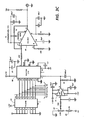
- Fig 3 is a schematic diagram of the memory comprising RAM 60 and PROM 61, addressed through buffers 62 - 65. Data are loaded into the memory through buffer 66. Data are taken out through buffer 67, which is enabled from start-of-scan to end-of-scan, and converted into a zero to one volt analog voltage in D/A converter 68 for input to amplifier 69, which, in turn, generates a zero to five volt signal to drive the acousto-optical facet tracker.
- a dummy input representing a constant gray value is generated at register 70 and applied to the amplifier 69 through D/A converter 68 to maintain all operating voltages in the following circuits in their normal operating ranges.
- Unity-gain amplifier 71 uses a voltage divider comprising resistors 84, 85 to generate the minus two volt reference voltage of a D/A converter.
- the data are written into memory 60, and the same word is immediately read out to the buffer 67.
- the operate mode no data are written in.
- the memory contents are sent out, as stored, to the buffer.
- Fig 4 is a schematic diagram of the modulator controller circuit, the main component of which is the acousto-optic modulator driver 80.
- the zero to five volt output from amplifier 69 of Fig 3 is shifted to a more positive voltage by zener diodes 81, 82, 83 to about positive 2 to 7 volts, and applied as the signal input to the driver 80, while a voltage divider reference is adjusted to plus 2 volts by potentiometer 81 at the other input.
- the driver 80 amplifies the voltage , resulting in an output which varies from approximately 2 volts to 26 volts.
Landscapes
- Engineering & Computer Science (AREA)
- Multimedia (AREA)
- Signal Processing (AREA)
- Facsimile Scanning Arrangements (AREA)
- Laser Beam Printer (AREA)
- Dot-Matrix Printers And Others (AREA)
- Mechanical Optical Scanning Systems (AREA)
Applications Claiming Priority (2)
| Application Number | Priority Date | Filing Date | Title |
|---|---|---|---|
| US06/880,517 US4751523A (en) | 1986-06-30 | 1986-06-30 | Laser scanner power compensation circuit |
| US880517 | 1986-06-30 |
Publications (3)
| Publication Number | Publication Date |
|---|---|
| EP0251740A2 true EP0251740A2 (fr) | 1988-01-07 |
| EP0251740A3 EP0251740A3 (en) | 1988-07-20 |
| EP0251740B1 EP0251740B1 (fr) | 1992-03-11 |
Family
ID=25376451
Family Applications (1)
| Application Number | Title | Priority Date | Filing Date |
|---|---|---|---|
| EP87305726A Expired EP0251740B1 (fr) | 1986-06-30 | 1987-06-26 | Appareil de balayage pour la reproduction |
Country Status (4)
| Country | Link |
|---|---|
| US (1) | US4751523A (fr) |
| EP (1) | EP0251740B1 (fr) |
| JP (1) | JP2533878B2 (fr) |
| DE (1) | DE3777259D1 (fr) |
Cited By (4)
| Publication number | Priority date | Publication date | Assignee | Title |
|---|---|---|---|---|
| EP0420573A3 (en) * | 1989-09-26 | 1991-08-07 | Canon Kabushiki Kaisha | Light beam driving apparatus |
| EP0484924A3 (en) * | 1990-11-07 | 1992-11-25 | Canon Kabushiki Kaisha | Image signal correcting circuit device for use in image data processing apparatus |
| US5386253A (en) * | 1990-04-09 | 1995-01-31 | Rank Brimar Limited | Projection video display systems |
| EP1175083A3 (fr) * | 2000-03-28 | 2004-05-19 | Noritsu Koki Co., Ltd. | Appareil à balayage de faisceau laser et son utilisation dans une imprimante photographique |
Families Citing this family (7)
| Publication number | Priority date | Publication date | Assignee | Title |
|---|---|---|---|---|
| JP3004991B2 (ja) * | 1988-04-18 | 2000-01-31 | キヤノン株式会社 | 画像処理装置 |
| JP2771822B2 (ja) * | 1988-10-21 | 1998-07-02 | 株式会社リコー | 光照射画像形成装置 |
| US4992890A (en) * | 1989-03-17 | 1991-02-12 | Intergraph Corporation | System for plotting and scanning graphic images |
| US5157522A (en) * | 1991-04-01 | 1992-10-20 | Eastman Kodak Company | Method and apparatus for providing correction of hologon transmission efficiency variations |
| US5166944A (en) * | 1991-06-07 | 1992-11-24 | Advanced Laser Technologies, Inc. | Laser beam scanning apparatus and method |
| US5281979A (en) * | 1992-11-04 | 1994-01-25 | Eastman Kodak Company | Laser printer calibration |
| US20020126199A1 (en) * | 2000-06-06 | 2002-09-12 | Eastman Kodak Company | Method and apparatus for correcting non-uniformity in digital images created on a raster scan film recorder |
Family Cites Families (7)
| Publication number | Priority date | Publication date | Assignee | Title |
|---|---|---|---|---|
| GB837778A (en) * | 1956-06-19 | 1960-06-15 | Logetronics Inc | Photographic method and apparatus |
| US3564133A (en) * | 1967-01-16 | 1971-02-16 | Itek Corp | Transformation and registration of photographic images |
| US3848087A (en) * | 1973-10-29 | 1974-11-12 | Rca Corp | Optical scanner control system |
| GB1515606A (en) | 1975-12-23 | 1978-06-28 | Ibm | Electrophotographic apparatus |
| JPS56102853A (en) * | 1980-01-21 | 1981-08-17 | Dainippon Screen Mfg Co Ltd | Metho for pretreating image signal of image copying apparatus |
| JPS5911061A (ja) * | 1982-07-09 | 1984-01-20 | Canon Inc | 画像表示装置 |
| JPS60120663A (ja) * | 1983-12-03 | 1985-06-28 | Matsushita Electric Ind Co Ltd | レ−ザ記録装置 |
-
1986
- 1986-06-30 US US06/880,517 patent/US4751523A/en not_active Expired - Fee Related
-
1987
- 1987-06-25 JP JP62159539A patent/JP2533878B2/ja not_active Expired - Lifetime
- 1987-06-26 EP EP87305726A patent/EP0251740B1/fr not_active Expired
- 1987-06-26 DE DE8787305726T patent/DE3777259D1/de not_active Expired - Fee Related
Cited By (7)
| Publication number | Priority date | Publication date | Assignee | Title |
|---|---|---|---|---|
| EP0420573A3 (en) * | 1989-09-26 | 1991-08-07 | Canon Kabushiki Kaisha | Light beam driving apparatus |
| US5151910A (en) * | 1989-09-26 | 1992-09-29 | Canon Kabushiki Kaisha | Light quantity control device |
| US5386253A (en) * | 1990-04-09 | 1995-01-31 | Rank Brimar Limited | Projection video display systems |
| EP0484924A3 (en) * | 1990-11-07 | 1992-11-25 | Canon Kabushiki Kaisha | Image signal correcting circuit device for use in image data processing apparatus |
| US5262873A (en) * | 1990-11-07 | 1993-11-16 | Canon Kabushiki Kaisha | Image signal correcting in image data processing requiring only small memory capacity |
| EP0687101A1 (fr) * | 1990-11-07 | 1995-12-13 | Canon Kabushiki Kaisha | Circuit de correction de signaux d'image utilisé dans un appareil de traitement de données d'image |
| EP1175083A3 (fr) * | 2000-03-28 | 2004-05-19 | Noritsu Koki Co., Ltd. | Appareil à balayage de faisceau laser et son utilisation dans une imprimante photographique |
Also Published As
| Publication number | Publication date |
|---|---|
| JPS6326066A (ja) | 1988-02-03 |
| US4751523A (en) | 1988-06-14 |
| EP0251740A3 (en) | 1988-07-20 |
| JP2533878B2 (ja) | 1996-09-11 |
| DE3777259D1 (de) | 1992-04-16 |
| EP0251740B1 (fr) | 1992-03-11 |
Similar Documents
| Publication | Publication Date | Title |
|---|---|---|
| US4400740A (en) | Intensity control for raster output scanners | |
| US4853710A (en) | Imaging by laser beam scanning | |
| EP0251740B1 (fr) | Appareil de balayage pour la reproduction | |
| US4663760A (en) | Semiconductor laser output control device | |
| US4893136A (en) | Arithmetically computed motor hunt compensation for flying spot scanners | |
| EP0021831A1 (fr) | Circuit d'horloge pour signaux d'image et procédé de fonctionnement d'un dispositif de visualisation à trames | |
| JP2743408B2 (ja) | レーザビームの走査速度補正方式 | |
| US5212570A (en) | Pixel clock phase locked loop for a laser scanner | |
| US5111311A (en) | Image reading apparatus with black level correction | |
| CA1116226A (fr) | Appareil pour corriger les erreurs de positionnement d'un polygone servant a l'exploration au laser, et methode connexe | |
| JPH0528941B2 (fr) | ||
| US4687919A (en) | A lighting control device in manuscript reproduction equipment | |
| GB2190768A (en) | Intensity control in a raster scanner | |
| JPH0933832A (ja) | 光走査装置および光走査装置におけるレーザビーム変調方法 | |
| US4876556A (en) | Beam recorder with a temperature sensor for light quantity control | |
| EP0375434A2 (fr) | Imprimantes numériques | |
| JPS6354273B2 (fr) | ||
| JP3048613B2 (ja) | 画像読取装置 | |
| US5671078A (en) | Accurate laser power control for dual/multiple beams | |
| US5450118A (en) | Image forming apparatus | |
| US5331432A (en) | Image forming apparatus | |
| JP3165707B2 (ja) | 光走査型画像形成装置 | |
| JPS6333347B2 (fr) | ||
| JPS6365769A (ja) | 画像処理装置 | |
| Helmberger et al. | Correction of axial deflection errors in rotating mirror systems |
Legal Events
| Date | Code | Title | Description |
|---|---|---|---|
| PUAI | Public reference made under article 153(3) epc to a published international application that has entered the european phase |
Free format text: ORIGINAL CODE: 0009012 |
|
| AK | Designated contracting states |
Kind code of ref document: A2 Designated state(s): DE FR GB IT |
|
| PUAL | Search report despatched |
Free format text: ORIGINAL CODE: 0009013 |
|
| AK | Designated contracting states |
Kind code of ref document: A3 Designated state(s): DE FR GB IT |
|
| RHK1 | Main classification (correction) |
Ipc: H04N 1/036 |
|
| 17P | Request for examination filed |
Effective date: 19890119 |
|
| 17Q | First examination report despatched |
Effective date: 19910225 |
|
| GRAA | (expected) grant |
Free format text: ORIGINAL CODE: 0009210 |
|
| AK | Designated contracting states |
Kind code of ref document: B1 Designated state(s): DE FR GB IT |
|
| REF | Corresponds to: |
Ref document number: 3777259 Country of ref document: DE Date of ref document: 19920416 |
|
| ET | Fr: translation filed | ||
| ITF | It: translation for a ep patent filed | ||
| PLBE | No opposition filed within time limit |
Free format text: ORIGINAL CODE: 0009261 |
|
| STAA | Information on the status of an ep patent application or granted ep patent |
Free format text: STATUS: NO OPPOSITION FILED WITHIN TIME LIMIT |
|
| 26N | No opposition filed | ||
| PGFP | Annual fee paid to national office [announced via postgrant information from national office to epo] |
Ref country code: FR Payment date: 19990610 Year of fee payment: 13 |
|
| PGFP | Annual fee paid to national office [announced via postgrant information from national office to epo] |
Ref country code: GB Payment date: 19990623 Year of fee payment: 13 |
|
| PGFP | Annual fee paid to national office [announced via postgrant information from national office to epo] |
Ref country code: DE Payment date: 19990626 Year of fee payment: 13 |
|
| PG25 | Lapsed in a contracting state [announced via postgrant information from national office to epo] |
Ref country code: GB Free format text: LAPSE BECAUSE OF NON-PAYMENT OF DUE FEES Effective date: 20000626 |
|
| GBPC | Gb: european patent ceased through non-payment of renewal fee |
Effective date: 20000626 |
|
| PG25 | Lapsed in a contracting state [announced via postgrant information from national office to epo] |
Ref country code: FR Free format text: LAPSE BECAUSE OF NON-PAYMENT OF DUE FEES Effective date: 20010228 |
|
| REG | Reference to a national code |
Ref country code: FR Ref legal event code: ST |
|
| PG25 | Lapsed in a contracting state [announced via postgrant information from national office to epo] |
Ref country code: DE Free format text: LAPSE BECAUSE OF NON-PAYMENT OF DUE FEES Effective date: 20010403 |
|
| PG25 | Lapsed in a contracting state [announced via postgrant information from national office to epo] |
Ref country code: IT Free format text: LAPSE BECAUSE OF NON-PAYMENT OF DUE FEES;WARNING: LAPSES OF ITALIAN PATENTS WITH EFFECTIVE DATE BEFORE 2007 MAY HAVE OCCURRED AT ANY TIME BEFORE 2007. THE CORRECT EFFECTIVE DATE MAY BE DIFFERENT FROM THE ONE RECORDED. Effective date: 20050626 |