EP0253264A2 - Circuit de codage en binaire pour OCR - Google Patents
Circuit de codage en binaire pour OCR Download PDFInfo
- Publication number
- EP0253264A2 EP0253264A2 EP87109708A EP87109708A EP0253264A2 EP 0253264 A2 EP0253264 A2 EP 0253264A2 EP 87109708 A EP87109708 A EP 87109708A EP 87109708 A EP87109708 A EP 87109708A EP 0253264 A2 EP0253264 A2 EP 0253264A2
- Authority
- EP
- European Patent Office
- Prior art keywords
- binary
- signal
- circuit
- threshold
- output
- Prior art date
- Legal status (The legal status is an assumption and is not a legal conclusion. Google has not performed a legal analysis and makes no representation as to the accuracy of the status listed.)
- Granted
Links
Images


Classifications
-
- G—PHYSICS
- G06—COMPUTING OR CALCULATING; COUNTING
- G06K—GRAPHICAL DATA READING; PRESENTATION OF DATA; RECORD CARRIERS; HANDLING RECORD CARRIERS
- G06K7/00—Methods or arrangements for sensing record carriers, e.g. for reading patterns
- G06K7/10—Methods or arrangements for sensing record carriers, e.g. for reading patterns by electromagnetic radiation, e.g. optical sensing; by corpuscular radiation
- G06K7/10544—Methods or arrangements for sensing record carriers, e.g. for reading patterns by electromagnetic radiation, e.g. optical sensing; by corpuscular radiation by scanning of the records by radiation in the optical part of the electromagnetic spectrum
- G06K7/10821—Methods or arrangements for sensing record carriers, e.g. for reading patterns by electromagnetic radiation, e.g. optical sensing; by corpuscular radiation by scanning of the records by radiation in the optical part of the electromagnetic spectrum further details of bar or optical code scanning devices
- G06K7/10851—Circuits for pulse shaping, amplifying, eliminating noise signals, checking the function of the sensing device
-
- G—PHYSICS
- G06—COMPUTING OR CALCULATING; COUNTING
- G06V—IMAGE OR VIDEO RECOGNITION OR UNDERSTANDING
- G06V30/00—Character recognition; Recognising digital ink; Document-oriented image-based pattern recognition
- G06V30/10—Character recognition
- G06V30/16—Image preprocessing
- G06V30/162—Quantising the image signal
-
- G—PHYSICS
- G06—COMPUTING OR CALCULATING; COUNTING
- G06V—IMAGE OR VIDEO RECOGNITION OR UNDERSTANDING
- G06V30/00—Character recognition; Recognising digital ink; Document-oriented image-based pattern recognition
- G06V30/10—Character recognition
Definitions
- the present invention relates in general .to binary coding circuits of the type used for analog signals. More specifically, the present invention provides a binary coding circuit for quantizing the output of a photoelectric conversion cell in an optical character reader (OCR). It quantizes the photoelectric conversion cell output into a binary signal having two values corresponding to a background area and a character or symbol area.
- OCR optical character reader
- character as used herein includes any kind of character or symbol. Thus, the term includes, but is not limited to alpha-numeric characters, symbols, Japanese “kana”, etc.
- symbol includes but is not limited to bar codes, etc.
- Characters are often printed black on white paper. The characters can be discriminated from blank space by discerning a difference between white and black. However, the paper which forms the background of the characters is not always white. This makes it more difficult to discern between the character and background.
- the area where characters are printed is hereinafter referred to as a "character area”. In contrast, the blank space, where no character is printer is referred to as a "background area”.
- optical character reader is used in a broad sense to include various types of apparatus for optically reading characters imprinted on a surface.
- OCR optical character reader
- the surface to be read is illuminated with light.
- a lens system images light reflected from the surface onto a matrix of photoelectric conversion cells. These cells provide output signals that are responsive to the intensity of light on the cells.
- Output signals of the cells are converted by a binary coding circuit into binary signals indicating a character areas and a background areas. Characters are discriminated on the basis of the binary signal.
- Light incident on the photoelectric conversion cells varies in accordance with the imprinted characters. Because the characters are black and the background is white, the level of incident light varies corresponding to the existence of characters.
- Characters written on the paper may not always be imprinted evenly on a page being read.
- the output of a photoelectric conversion cell scanning the paper does not always take one of two values corresponding to black or-white. Rather, it may vary continuously and irregularly. Even if the characters are printed using type, a character may not be formed exactly the same each time. Also, characters vary from one another in shape and size, number of strokes, etc.
- the output of a photoelectric conversion cell may vary widely in an analog manner. Its output may change both spatially and temporally.
- the output does not simply take either one of a maximum value and a minimum value. Rather, the output continuously varies between the maximum and minimum values.
- a simple binary coding method for converting such an analog concentration signal into a binary signal is to compare it with a fixed threshold level.
- this binary coding method has a disadvantage in that the character area is often mistaken or misjudged for background area. Characters are often at least partially missed.
- the simple binary coding method has a further disadvantage in that the background area is often mistaken for character area.
- the characters may be defaced or obscured by stains between character lines, etc. If character recognition is made on the basis of the binary-coded data in the manner as described above, many errors result.
- threshold level refers to a value that is compared with the amplitude of a signal. As the result of comparison, an output signal of "0" or “1” " is generated.
- the "0" or “1” constitutes a binary code. If the threshold level is fixed, the aforementioned problems exist. Accordingly, a fixed threshold level can not be used unless the characters are extremely simple.
- Japanese Patent Publication No. 37952/1985 discloses a technique in which four different thresholds are used to binary code the output of a photoelectric conversion cell. Of the four thresholds, one which may provide an optimum result of binary coding is selected.
- the characters have line widths that vary from character to character.
- the line width of a character printed in Gothic type is large in comparison with the same character printed in a different "font". Even for characters printed with the same font, the line width of characters may vary from character to character depending on calligraphic style. Further, some lines of a particular character may be thicker than other lines of the same character. For example, vertical lines of a certain character may be thicker than horizontal lines of the same character, or vice versa.
- the width of one line in a character may vary from one end of the line to the other.
- an optimum threshold is selected on the basis of the change of the line width. A large number of arithmetic operations are required to do this. It can be said that an average line width of characters printed using a certain type font is generally within a predetermined range.
- line width can be computed.
- number of black points means the number of black meshes (picture elements) in the whole picture scene.
- number of surrounding points means the number of black picture elements on the boundary of white and black areas.
- a character is simply constituted by a horizontal bar "-" which includes black picture elements of r and g in number arranged in rows and columns respectively ( q » r).
- the number of black points is r x q, and the number of surrounding points is (2q + 2r - 2).
- the real line width of the character is r. Accordingly, the line width W as defined by the above equation is approximately r/2. It may be said that the line width W is defined as the half width of the real character line.
- the average line width of characters printed in a certain type font can be obtained by repeating such arithmetic operations on all characters. Assume that W is known to be 1.5 with respect to a certain group of characters belonging to a certain dictionary pattern. Assume that a typescript is made up of the group of characters contained in the dictionary pattern. The typescript is optically read and the resulting signal is binary coded by comparing it with four separate and distinct threshold levels Ui, U 2 , U 3 and U 4 . Four binary patterns can be thus obtained to thereby determine black-and-white picture elements. With respect to the four patterns, the number of black points and the number of surrounding points are counted to thereby calculate the line width.
- the threshold level is too low, the number of black points is excessively increased so that the line becomes thick, that is, the line width becomes large. If the threshold level is too high, the number of white points is excessively increased so that the line becomes thin, that is, the line width becomes small.
- four values of line width, Wi, W 2 , Ws, and W4 can be calculated. Because the average line width W of the characters contained in the dictionary pattern is predetermined, an optimum one that approaches W is selected from the four values of line width, Wi, Wz, W 3 and W 4 . Accordingly, one binary pattern is selected from the four binary-coding patterns on the basis of the thus selected optimum line width.
- binary coding is performed by use of four threshold levels to thereby calculate values of line width.
- the calculated values of line width are compared with a predetermined value of line width to thereby select an optimum one of the calculated values of line width which is the most approximate to the predetermined one.
- This method lacks reliability and a large number of arithmetical operations are required.
- the number of black points and the number of surrounding points should be counted according to every pattern.
- the time required for counting the number of surrounding points is long, because the boundary of white and black must be detected.
- the line width in the dictionary pattern should be predetermined. There is one of the most difficult aspects of this technique. It is necessary to apply it to various kinds of characters. That is, the range of use is limited to specific kinds of characters. Any character should be read even if the character has any line width.
- a further disadvantage occurs with the four threshold arrangement. Although four thresholds U 1 -U 4 are used, those thresholds are used in the alternative. Once a threshold is selected, it is used for the whole picture. The local characteristics of the picture are not considered. If the character is so complex that wo peaks are near to each other, the output between the peaks is not zero. Rather, the output is "drawn up” by the two peaks. It is difficult to discriminate the intermediate output from the peaks. Accordingly, the space between two lines becomes “smeared".
- the binary coding circuit according to the Japanese Patent Publication No. 37952/1985 has the disadvantages of large circuit scale and high cost. Also, real time processing and use for all types of characters are impossible.
- the present invention provides a binary coding circuit which is simple in construction, yet capable of determining an optimum threshold level. Furthermore, it can binary code in real time. It can read any type of characters without mistake. It securely identifies the "black" portions of picture elements.
- the output of the photoelectric conversion cell is proportional to the intensity of light impinging thereon.
- the cell output becomes large for a black picture element and becomes small for a white one. It is sufficient that portions corresponding to peaks of the output can be detected.
- peak includes large peaks, small peaks, wide peaks, and narrow peaks. It is considered that large and wide peaks correspond to bold-faced characters and that small and narrow peaks correspond to light-faced characters.
- the inequalities can be used as simple comparison inequalities.
- the necessary and sufficient condition that each of ⁇ and T ' can take an arbitrary value is removed.
- the function may have a peak value if the inequalities (1) and (2) are satisfied on the basis of fixed ⁇ and ⁇ '.
- the peak can be almost perfectly detected from the inequalities (1) and (2) as long as ⁇ and ⁇ ' are selected adequately.
- the inequality (3) is equivalent to the two inequalities (1) and (2). That is, the inequality (3) is equivalent to the combination of inequalities (1) and (2).
- ⁇ (t) does not always take a peak value even if it is a positive value.
- the peak value can be almost perfectly detected when ⁇ (t) is positive, as long as ⁇ and r' are selected adequately.
- the binary coding circuit according to the present invention includes:
- Figure 1 is a block diagram of a binary coding circuit according to the present invention.
- the output A of a photoelectric conversion cell is generated unit by unit corresponding to picture elements.
- the cell output is a function of light intensity.
- the relationship of cell signal output to light intensity can be of either sense as a matter of design choice.
- the output may be high for a white picture element is selected and low for a black picture element, or the output may be high for a black picture element and low for a white one.
- the output can be arbitrarily oriented by using inverter circuitry. We assume henceforth that the photoelectric conversion cell output is high when a character, i.e., a black picture element is being "viewed".
- a delay circuit 1 generates at least three delayed signals Qi,...Q m ,...Q n .
- One signal Q m adequate for binary coding is selected from among those delayed signals.
- Delayed signals other than the signal Q m which are (n-1) in number, are linearly coupled or the maximum is selected from the delayed signals, so that a threshold H is determined. This function is carried out by a threshold determining circuit 2.
- the threshold can be determined by linear coupling.
- the linear coupling coefficient is adequately predetermined, and n is not less than 3, that is, n ⁇ 3.
- Q m is a signal to be binary-coded
- the signal may be amplified by an amplifier circuit 3 if the signal from the delay circuit 1 is low in amplitude and high in impedance. Amplification may be omitted if not necessary.
- Threshold H is determined by threshold determining circuit 2.
- the threshold is locally determined so as to be changed temporally. This threshold is quite different from the conventionally fixed threshold. This threshold is also different from the threshold common to the whole picture, as disclosed in Japanese Patent Publication No. 37952/1985.
- the threshold according to the present invention is a locally variable threshold level which is individually produced from each local signal delayed or effectively advanced.
- the threshold H is then compared with Qz. Such comparison is equivalent to the equation (4) or (3). If necessary, the threshold level H may be amplified by an amplifier circuit 4.
- S represents a signal to be binary-coded, obtained by amplifying Q m (or without amplifying Q m ).
- H represents a threshold signal obtained by amplifying the threshold level (or without amplifying it). To minimize confusion, the reference "H" is used both before and after amplification.
- a comparator circuit 5 compares S and H. If the signal S has a peak value (if the signal S represents a black picture element) S is larger than H (S > H). If the signal S represents a white picture element, S is smaller than H (S ⁇ H).
- Figure 2 is a block diagram of the binary coding circuit for use when the input analog signal has the waveform which is upwards convex. This is the case wherein the output becomes high for a black picture element.
- the photoelectric conversion cell output A has several positive peaks at various points.
- the three delay times Ti, T 2 and T 3 are different from each other. 0 ⁇ T 1 ⁇ T 2 ⁇ T 3 (8)
- the signal Q 1 may be the original output signal per se. In other words, the delay time T 1 may be zero.
- the value of (T 3 -T 2 ) may be equal to the value of (T 2 -T 1 ).
- a threshold level is determined on the basis of the advanced signal Q 1 and the delayed signal Q 3 .
- an OR circuit 21 is used.
- the expression "OR circuit” as referring to OR circuit 21 is not necessarily used in its precise manner. Rather, the words “OR circuit” may include a circuit for identifying the maximum value in the same manner as the equation (7).
- H max ⁇ Qi, Q 3 ⁇ (9)
- Q 1 and Q 3 are analog quantities and therefore the term "OR circuit" cannot be exactly defined for those two analog quantities.
- the circuit for performing such an arithmetical operation as set forth in equation (9) is referred to as an "OR circuit".
- the output of the circuit is Q max .
- the circuit has been defined so as to include the functions called for by equation (9).
- Signal Q 2 passes through the amplifier circuit 3 where it is amplified and offset.
- the amplified and offset signal from amplifier 3 is coupled to one input terminal of the comparator circuit 5 as a binary coding target signal.
- the signals S and H are compared with each other. If the signal S is in a peak state, S is larger than H. If the signal S is not in a peak state, S is smaller than H.
- curve 100 shows the output of the photoelectric conversion cell having a peak.
- Curves 102, 104 and 106 shows output signals Qi, Q 2 and Q 3 respectively delayed for delay times T 1 , T 2 and T 3 . These output signals have the same waveform but the time axes of the signals are differently shifted.
- the beginning point of the waveform is denoted by P and the end point of the waveform is denoted by R.
- the intersection of Q 1 and Q 2 is denoted by K and the intersection of Q 2 and Q 3 is denoted by M.
- the intersection of Q 3 and Q 1 is denoted by L.
- the threshold level H does not take a constant voltage.
- the binary coding circuit according to the present invention is different from the conventional binary coding circuit in this respect.
- the term "level" may be used in its precise manner because it is variable temporally.
- the threshold H is the maximum value of Q 1 and Q 3 , so that H is equal to Q 1 before the point L and then H is equal to Q 3 after the point L.
- the threshold H is expressed by the curve PKLMR.
- Reference numeral 108 refers to the waveform of the binary signal B. Between the points K' and M' which correspond to the points K and M, the signal B takes the value of "1". Between the points P' and K' and between the points M' and R', the signal B takes the value of "0".
- Fig. 3(b) shows the waveforms of Q 1 , Q 2 and Q 3 after such a procedure.
- the amplification factor for Q 2 larger than those for Q 1 and Q 3 . Accordingly, the amplitude of Q 2 is larger, but contrarily, Q 2 is offset by ⁇ downward from Q 1 and Q 3 .
- the value P 2 of Q 2 is lowered by downward from the value P 1 of Q 1 in the start stage.
- the value R 2 of Q 2 is lowered by ⁇ downward from the value R 3 of Q 3 in the end stage.
- the waveforms of Q 1 and Q 3 , the threshold H and the intersection L of Q 1 and Q 3 are not changed, but the binary coding target signal S is changed.
- the amplification factor is represented by ⁇ ( ⁇ > 1 ).
- the change of the binary coding target signal S is expressed as follows: Q 2 ⁇ ⁇ Q 2 - ⁇ (10)
- the comparative output becomes positive against the flat signal because of ⁇ -1 > 0.
- the binary output B takes the value of "1" and there is an erroneous judgment.
- the offset - A can prevent such a malfunction.
- the depth - ⁇ of the offset is determined by judging from the amplification factor ⁇ and the necessity of preventing the malfunction to the height of the flat level Q.
- Figure 3(b) shows the case where the offset is not established.
- the offset is essential.
- the offset may be used even though its use is not essential.
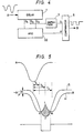
- Figure 4 is a block diagram of the binary coding circuit for use when the input signal has a waveform which is downward convex.
- the operation of the binary coding circuit of Figure 4 is similar to that of Figure 2, except that the relation of level is reversed and an AND circuit 22 is used as a threshold determining circuit.
- Q 1 , Q 2 and Q 3 are output signals delayed for times T 1 , T 2 , and T 3 , respectively.
- a binary coding target signal S is formed from Q 2
- threshold H is formed from Q 1 and Q 3 .
- Figure 5 includes graphs of waveforms explaining the operation of the circuit of Figure 4.
- the upper portion of Figure 5 shows the output of the photoelectric conversion cell.
- the output signal has a negative peak.
- the output signal is delayed for times T 1 , T 2 and T 3 to thereby generate waveforms Q 1 , Q 2 and Q 3 as shown in center portion of Figure 5.
- Q 2 is amplified and offset by the positive offset + ⁇ .
- the threshold H is expressed by the minimum value of Q 1 and Q 3 .
- H min ⁇ Q 1 , Q 3 ⁇ (13)
- the AND circuit 22 is required for defining the threshold H as expressed by the equation (13).
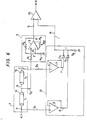
- Figure 6 is a circuit diagram of a binary coding circuit according to one embodiment of the present invention.
- the output A of a photoelectric conversion cell is applied to a delay circuit constituted by delay lines 11 and 12.
- the delay lines are used as the most simple method for delaying an analog signal without changing the waveform thereof.
- the delay lines have delay times t 1 and t 2 , respectively.
- the delay lines are connected in series.
- the delay at the input point a of the delay line 11 is 0, the delay at the junction point b between the delay lines 11 and 12 is t i , and the delay at the output point c of the delay line 12 is (t 1 + t 2 )
- a signal Q 1 from the point a and a signal Q 3 from the point c are respectively connected to non- inversion input terminals of differential amplifiers 6 and 7 in an OR circuit 21. Inversion input terminals of the respective differential amplifiers 6 and 7 are respectively connected to output terminals thereof.
- These two differential amplifiers 6 and 7 function as a voltage follower. A voltage is not amplified between the input and output but the impedance is lowered. Accordingly, voltages at the output points d and e of the differential amplifiers 6 and 7 are equal to the voltages of the input signals Q 1 and Qz.
- the output signals of the differential amplifiers 6 and 7 are respectively passed through diodes D1 and D2 and then connected to an inversion input terminal of a comparator 51.
- the inversion input is grounded through a resistor R5.
- the respective cathodes of the two diodes D1 and D2 are connected to each other for the purpose of performing OR operation.
- the signals at the points d and e have analog quantities. The higher one is selected from the signals appears at the point i. A lower one of the signals has no influence on the point i because the diode corresponding to the signal is reversely biased.
- the voltage at the point i is a little lower than the maximum value at the points d and e, because the voltage is lowered by about 0.6 V due to the PN junction of the diode.
- the offset value as described above can be adjusted by a variable resistor R4 in a differential amplifier 9. Offset adjusting resistor R4 has the dual purposes of compensating the lowering of voltage due to the pn junction in each of the diodes D1 and D2, and adjusting the offset value defined by the equations (10) -(12).
- the output Qz from the point b between the delay lines 11 and 12 is amplified and offset by the differential amplifier 9.
- a constant voltage V EE is connected to an intermediate terminal of variable resistor R4.
- a resistor R3 is connected to an inverting input terminal g of the differential amplifier 9.
- the signal Q 2 to be binary-coded is connected to a non-inverting input terminal f of differential amplifier 9 through a resistor R1 which is nearly equal in resistance value to a resistor R3.
- the output terminal h of the differential amplifier 9 is connected to the inverting input terminal g through a resistor R2.
- the offset of he output can be arbitrarily established by adjusting the resistor R4.
- the resistor R4 has the dual purposes of compensating the lowering of voltage due to the PN junction in each of diodes D1 and D2, and adjusting the offset value - A defined by the equations (10) - (12).
- the two signals S and H are applied to the two input terminals of the comparator 51.
- the binary signal B takes the value of "1" for the condition of S > H or takes the value of "0" for the condition of S ⁇ H.
- binary coding takes place as shown in the lower portions of Figures 3(a) and 3(b).
- This binary coding circuit does not use a fixed threshold level. Further, the circuit does not use a threshold level common to the whole picture. A variable threshold is locally determined by use of the local change of signal. Accordingly, if two types of analog signals respectively having a higher peak value and a lower peak value are continuously received, binary coding is perfected.
- the circuit is simple in construction but capable of accurate binary coding an analog input signal two a two-valued signal.
- the circuit is particularly applicable to optical character readers (OCRs) and bar code readers (BCRs). It is particularly well suited for use in portable OCRs and BCRs for point of sale (POS) automated reading where small size, low cost and a high speed are required and where the analog signal level may be unstable.
Landscapes
- Engineering & Computer Science (AREA)
- Physics & Mathematics (AREA)
- Electromagnetism (AREA)
- General Physics & Mathematics (AREA)
- Theoretical Computer Science (AREA)
- Computer Vision & Pattern Recognition (AREA)
- Multimedia (AREA)
- Health & Medical Sciences (AREA)
- General Health & Medical Sciences (AREA)
- Toxicology (AREA)
- Artificial Intelligence (AREA)
- Facsimile Image Signal Circuits (AREA)
- Character Input (AREA)
Applications Claiming Priority (2)
| Application Number | Priority Date | Filing Date | Title |
|---|---|---|---|
| JP160446/86 | 1986-07-08 | ||
| JP61160446A JPH0719275B2 (ja) | 1986-07-08 | 1986-07-08 | 二値化回路 |
Publications (3)
| Publication Number | Publication Date |
|---|---|
| EP0253264A2 true EP0253264A2 (fr) | 1988-01-20 |
| EP0253264A3 EP0253264A3 (en) | 1990-08-22 |
| EP0253264B1 EP0253264B1 (fr) | 1993-01-13 |
Family
ID=15715106
Family Applications (1)
| Application Number | Title | Priority Date | Filing Date |
|---|---|---|---|
| EP87109708A Expired - Lifetime EP0253264B1 (fr) | 1986-07-08 | 1987-07-06 | Circuit de codage en binaire pour OCR |
Country Status (5)
| Country | Link |
|---|---|
| US (1) | US4856076A (fr) |
| EP (1) | EP0253264B1 (fr) |
| JP (1) | JPH0719275B2 (fr) |
| CA (1) | CA1291265C (fr) |
| DE (1) | DE3783524T2 (fr) |
Cited By (2)
| Publication number | Priority date | Publication date | Assignee | Title |
|---|---|---|---|---|
| US4894727A (en) * | 1987-10-20 | 1990-01-16 | Ricoh Company, Ltd. | Image processing system and method |
| EP0268983B1 (fr) * | 1986-11-27 | 1993-02-03 | Sumitomo Electric Industries Limited | Circuit de codage binaire |
Families Citing this family (7)
| Publication number | Priority date | Publication date | Assignee | Title |
|---|---|---|---|---|
| US5001767A (en) * | 1987-11-30 | 1991-03-19 | Kabushiki Kaisha Toshiba | Image processing device |
| US5969325A (en) * | 1996-06-03 | 1999-10-19 | Accu-Sort Systems, Inc. | High speed image acquisition system and method of processing and decoding barcode symbol |
| US5861616A (en) * | 1996-10-01 | 1999-01-19 | Mustek Systems, Inc. | Method and device for recognizing a waveform of an analog signal |
| US6012640A (en) * | 1997-07-08 | 2000-01-11 | Intermec Ip Corporation | Rule based and fuzzy logic method and apparatus for processing reflectance signals from machine-readable symbols or images |
| US6016960A (en) * | 1997-07-08 | 2000-01-25 | Intermec Ip Corporation | Rule based method and apparatus for processing reflectance signals from machine-readable symbols or images |
| US6785344B1 (en) * | 2000-04-11 | 2004-08-31 | Terawave Communications, Inc. | Fast threshold determination for packet-multiplexed digital communication |
| US20050095565A1 (en) * | 2003-10-30 | 2005-05-05 | Steinberg Joel S. | Method of teaching mathematical operations and functions using a new numerical notation system |
Family Cites Families (8)
| Publication number | Priority date | Publication date | Assignee | Title |
|---|---|---|---|---|
| US3534334A (en) * | 1967-06-20 | 1970-10-13 | Ibm | Automatic control of a threshold in the digitization of an analog signal |
| US3987413A (en) * | 1975-01-22 | 1976-10-19 | Xerox Corporation | Detection system |
| JPS57150277A (en) * | 1981-03-13 | 1982-09-17 | Fuji Xerox Co Ltd | Image signal processing circuit |
| US4442544A (en) * | 1981-07-09 | 1984-04-10 | Xerox Corporation | Adaptive thresholder |
| US4430748A (en) * | 1981-09-21 | 1984-02-07 | Xerox Corporation | Image thresholding system |
| DE3174105D1 (en) * | 1981-12-23 | 1986-04-17 | Ibm | Method of recognizing characters in an optical document reader |
| US4468704A (en) * | 1982-10-28 | 1984-08-28 | Xerox Corporation | Adaptive thresholder |
| DE102006004922B4 (de) | 2006-02-01 | 2008-04-30 | Nanoscale Systems Nanoss Gmbh | Miniaturisiertes Federelement und Verfahren zu dessen Herstellung, Balkensonde, Rasterkraftmikroskop sowie Verfahren zu dessen Betrieb |
-
1986
- 1986-07-08 JP JP61160446A patent/JPH0719275B2/ja not_active Expired - Lifetime
-
1987
- 1987-07-06 DE DE8787109708T patent/DE3783524T2/de not_active Expired - Fee Related
- 1987-07-06 EP EP87109708A patent/EP0253264B1/fr not_active Expired - Lifetime
- 1987-07-07 US US07/070,733 patent/US4856076A/en not_active Expired - Fee Related
- 1987-07-07 CA CA000541489A patent/CA1291265C/fr not_active Expired - Lifetime
Cited By (2)
| Publication number | Priority date | Publication date | Assignee | Title |
|---|---|---|---|---|
| EP0268983B1 (fr) * | 1986-11-27 | 1993-02-03 | Sumitomo Electric Industries Limited | Circuit de codage binaire |
| US4894727A (en) * | 1987-10-20 | 1990-01-16 | Ricoh Company, Ltd. | Image processing system and method |
Also Published As
| Publication number | Publication date |
|---|---|
| DE3783524T2 (de) | 1993-05-13 |
| JPS6316393A (ja) | 1988-01-23 |
| EP0253264A3 (en) | 1990-08-22 |
| EP0253264B1 (fr) | 1993-01-13 |
| DE3783524D1 (de) | 1993-02-25 |
| JPH0719275B2 (ja) | 1995-03-06 |
| CA1291265C (fr) | 1991-10-22 |
| US4856076A (en) | 1989-08-08 |
Similar Documents
| Publication | Publication Date | Title |
|---|---|---|
| EP0797812B1 (fr) | Lecteurs de formes de donnees | |
| US4323772A (en) | Bar code reader system | |
| US5073954A (en) | Bar code location and recognition processing system | |
| EP0240767B1 (fr) | Lecteur à fente pour codes à bâtonnets | |
| US4910787A (en) | Discriminator between handwritten and machine-printed characters | |
| EP0419226B1 (fr) | Unité pour le traitement de signaux dans un lecteur de caractères à bâtonnets | |
| US5805740A (en) | Bar-code field detecting apparatus performing differential process and bar-code reading apparatus | |
| GB1584434A (en) | Wave shaping system | |
| DE69637397T2 (de) | Optischer Barcode Abtaster | |
| EP0253264A2 (fr) | Circuit de codage en binaire pour OCR | |
| US6102295A (en) | Method and apparatus for decoding symbols by declaring erasures of element characteristics | |
| US5637853A (en) | Reading indicia by analysis of different light reflecting portions based on signal-to-noise ratios | |
| US6098883A (en) | Method of estimating the mid-points of bar code elements | |
| US4751743A (en) | Optical character reader | |
| US4881188A (en) | Binary coding circuit | |
| CA1115842A (fr) | Detecteur optique de code de position a grande resolution pour information enregistree sur un support en partie sous forme intelligible | |
| US3900832A (en) | Bar code processing and detecting system | |
| US4078227A (en) | Threshold detector for optical character recognition system | |
| EP0505970B1 (fr) | Circuit pour détecter le niveau du blanc pour un balayeur optique | |
| JPH0119193B2 (fr) | ||
| JPH04251394A (ja) | バーコード読取装置 | |
| JPH0365583B2 (fr) | ||
| JPH10143608A (ja) | 文字読取装置 | |
| JPS627266A (ja) | 画像処理装置 | |
| JPH0363114B2 (fr) |
Legal Events
| Date | Code | Title | Description |
|---|---|---|---|
| PUAI | Public reference made under article 153(3) epc to a published international application that has entered the european phase |
Free format text: ORIGINAL CODE: 0009012 |
|
| AK | Designated contracting states |
Kind code of ref document: A2 Designated state(s): DE IT |
|
| PUAL | Search report despatched |
Free format text: ORIGINAL CODE: 0009013 |
|
| AK | Designated contracting states |
Kind code of ref document: A3 Designated state(s): DE IT |
|
| 17P | Request for examination filed |
Effective date: 19901113 |
|
| 17Q | First examination report despatched |
Effective date: 19910626 |
|
| GRAA | (expected) grant |
Free format text: ORIGINAL CODE: 0009210 |
|
| AK | Designated contracting states |
Kind code of ref document: B1 Designated state(s): DE IT |
|
| REF | Corresponds to: |
Ref document number: 3783524 Country of ref document: DE Date of ref document: 19930225 |
|
| ITF | It: translation for a ep patent filed | ||
| PLBE | No opposition filed within time limit |
Free format text: ORIGINAL CODE: 0009261 |
|
| STAA | Information on the status of an ep patent application or granted ep patent |
Free format text: STATUS: NO OPPOSITION FILED WITHIN TIME LIMIT |
|
| 26N | No opposition filed | ||
| PGFP | Annual fee paid to national office [announced via postgrant information from national office to epo] |
Ref country code: DE Payment date: 19950710 Year of fee payment: 9 |
|
| PG25 | Lapsed in a contracting state [announced via postgrant information from national office to epo] |
Ref country code: DE Effective date: 19970402 |
|
| PG25 | Lapsed in a contracting state [announced via postgrant information from national office to epo] |
Ref country code: IT Free format text: LAPSE BECAUSE OF NON-PAYMENT OF DUE FEES;WARNING: LAPSES OF ITALIAN PATENTS WITH EFFECTIVE DATE BEFORE 2007 MAY HAVE OCCURRED AT ANY TIME BEFORE 2007. THE CORRECT EFFECTIVE DATE MAY BE DIFFERENT FROM THE ONE RECORDED. Effective date: 20050706 |