EP0253786A1 - Kurzschlussschutz - Google Patents
Kurzschlussschutz Download PDFInfo
- Publication number
- EP0253786A1 EP0253786A1 EP87850187A EP87850187A EP0253786A1 EP 0253786 A1 EP0253786 A1 EP 0253786A1 EP 87850187 A EP87850187 A EP 87850187A EP 87850187 A EP87850187 A EP 87850187A EP 0253786 A1 EP0253786 A1 EP 0253786A1
- Authority
- EP
- European Patent Office
- Prior art keywords
- circuit
- output
- stage
- control
- component
- Prior art date
- Legal status (The legal status is an assumption and is not a legal conclusion. Google has not performed a legal analysis and makes no representation as to the accuracy of the status listed.)
- Granted
Links
- 230000001012 protector Effects 0.000 title claims abstract description 39
- 230000001681 protective effect Effects 0.000 claims abstract description 61
- 230000004044 response Effects 0.000 claims abstract description 15
- 230000008859 change Effects 0.000 claims abstract description 4
- 238000000034 method Methods 0.000 claims description 8
- 239000000306 component Substances 0.000 claims 59
- 230000003111 delayed effect Effects 0.000 description 3
- 230000002349 favourable effect Effects 0.000 description 2
- 230000009467 reduction Effects 0.000 description 2
- 230000009471 action Effects 0.000 description 1
- 230000003213 activating effect Effects 0.000 description 1
- 238000013459 approach Methods 0.000 description 1
- 238000010276 construction Methods 0.000 description 1
- 230000008878 coupling Effects 0.000 description 1
- 238000010168 coupling process Methods 0.000 description 1
- 238000005859 coupling reaction Methods 0.000 description 1
- 230000000694 effects Effects 0.000 description 1
- 230000004048 modification Effects 0.000 description 1
- 238000012986 modification Methods 0.000 description 1
Images

Classifications
-
- H—ELECTRICITY
- H03—ELECTRONIC CIRCUITRY
- H03K—PULSE TECHNIQUE
- H03K19/00—Logic circuits, i.e. having at least two inputs acting on one output; Inverting circuits
- H03K19/003—Modifications for increasing the reliability for protection
- H03K19/00315—Modifications for increasing the reliability for protection in field-effect transistor circuits
-
- H—ELECTRICITY
- H03—ELECTRONIC CIRCUITRY
- H03K—PULSE TECHNIQUE
- H03K19/00—Logic circuits, i.e. having at least two inputs acting on one output; Inverting circuits
- H03K19/0008—Arrangements for reducing power consumption
- H03K19/0013—Arrangements for reducing power consumption in field effect transistor circuits
Definitions
- the present invention relates to short circuit protectors in electrical circuits.
- the invention is primarily intended for output stages having two series connected transistors, the conductive capacity of which is controlled complementally such as to generate on an output between the transistors an output signal with a potential varying in response to the potential of an input signal.
- the invention is also applicable to certain other circuits, with an output between two series connected components with controllable conductive capacity, for limiting damaging currents through the components in case of a certain kind of short circuit or too low ohmic load on the outputs.
- the invention is particularly suitable for realization in integrated circuits of the MOS type both NMOS as well as CMOS.
- an overload and short circuit protector can protect both transistors a) for overload, b) for short circuiting of the output to the high feed voltage, c) for short circuiting of the output to the low feed voltage.
- the short circuit and overload protection does not limit the potential difference which can be achieved on the output by different types of complemental control of the conductivity state of both transistors.
- the overload and short circuit protection does not load the signal source supplying the circuit input signals, e.g. by short circuiting or lowering the input impedance of the circuit input.
- the short circuit protection and overload protection are selective, i.e., that they come into operation only during a short-circuiting or overloading situation.
- all short circuiting situations do not always have the consequence of damage to the transistors.
- the short circuit state can at least temporarily be more or less damaging, nor even ot cause any immediate risk of the damage to one of the transistors.
- the present invention can be said to be based on the use of at least one circuit or stage including two controllable components, preferably two series connected transistors.
- the protective circuit or stage is coupled into the circuit to be protected so that the conductive capacity of one of the controllable components is substantially controlled by the potential on the output of the circuit to be protected, with the conductive capacity of the second controllable component substantially depending on the input signal to the circuit to be protected.
- the protective circuit or stage is coupled into the circuit to be protected so that it achieves a substantial change in the conductive capacity of one of the output stage transistors or the like component, if, and only if, both transistors or the like of the protective circuit or stage become conductive simultaneously.
- a protective circuit or stage is preferably arranged for each output stage transistor or the like, as well as a control stage for each protective circuit or stage.
- Figure 1 illustrates a known transistor stage in CMOS techniques with a p-channel transistor coupled in series with an n-channel transistor.
- the stage has an input IN connected to both transistors, and an output OUT connected between the transistors.
- the n-channel transistor is on and the p-channel transistor is off.
- the potential on the input is sufficiently low in relation to the feed voltages, the p-channel transistor is on instead, and the n-channel transistor is off. Due to one transistor being of the p-channel type and the other of the n channel type, the conductivity of both transistors can be controlled complementally directly via a common input IN.
- Figure 2 illustrates a known transistor stage in NMOS technique with two principly alike series connected n-channel transistors.
- the stage has an output OUT connected between the transistors. Due to both transistors being of the same type, their conductivity cannot be controlled complementally directly viaa common input.
- the stage in Figure 2 therefore has in principle two inputs, IN and intended for complemental input signals, i.e. when the potential on one transistor input IN is comparatively low, the potential on the other input shall be comparatively high, and vice versa.
- FIG. 1 or 2 When at least one transistor stage according to Figure 1 or 2 is implemented as an output stage with the capacity of supplying a comparatively high output current or output power, a buffer or control stage is generally required to generate suitable input signals to the output stage, these signals coming from logical circuits in MOS technique.
- Figures 3 and 4 illustrate examples of how to drive an output stage according to Figur 1 or 2 with the aid of buffer or control stages.
- the circuit in Figure 3 has an input IN and an output OUT and three apparently alike cascade connected transistor stages, each of which is in principle of the same type as in Figure 1. Actually, however, the transistors are normally dimensioned differently, the transistors in the output stage, i.e. the transistor stage nearest the output being the greatest.
- the cascade connection enables the load on the signal to be small simultaneoulsy as the circuit can drive a large output current.
- the current in Figure 4 has an input IN and an output OUT and two cascade connected control or buffer stages. Since both the series connected transistors, of the same type in the output stage, shall have complementally varying control signals to obtain complementally varying conductivity, the upper transistor in the output stage is coupled directly to the first buffer or control stage output, while the lower transistor in the output stage is coupled directly to the second buffer or control stage output.
- an output stage according to Figure 1 or 2 included, for example, in a circuit according to Figure 3 or 4, is allowed to drive a load other than the one it is dimensioned for, or its output is shortcircuited to one or other of the feed voltages, i.e., the high VDD or the low VSS, of which one can be ground potential, or to another feed voltage for a circuit coupled to the output OUT, there is a risk that in response to the input signal potential one of the transistors in the output stage will be subjected to a current, which is considerably greater than the maximum permitted, and this can permanently damage the transistor.
- the input signal has a potential such that it strives to control the conductivity of the output stage transistors so that the output is given a low potential simultaneously as the output is short circuited to the high feed voltage VDD or to a high feed voltage for another circuit coupled to the output OUT.
- the risk of permanent damage to the transistor in the output stage is considerably less, or even non-existant, if the input signal has a potential such that it strives to control the conductivities of the output stage transistors so that the output OUT is given a high potential, simultaneously as the output is short circuited to the high feed voltage.
- the risk is less, or in favourable cases non-existent, if the input signal has a potential such that it strives to control the conductivities of the output stage transistors so that the output OUT is given a low potential simultaneously as the output is short circuited to the low feed voltage.
- the risks of damage are similar to those in short circuiting, but they decrease with increasing load resistance.
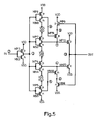
- the embodiments of short circuit protected circuits according to the invention, which are illustrated in Figures 5 and 6, are based on this knowledge of the damage risks.
- the short circuits protected circuit illustrated in Figure 5 includes an output stage with two series connected output stage components in the form of the transistors MP10 and MN1.
- a circuit output OUT is connected to a point 10 between the series connected transistors in the output stage.
- a circuit input IN is connected at a point 2 to both the transistors MP3 and MN3 in an input stage.
- For controlling the conductivity of the transistor MN10 there is a first buffer or control stage including transistors MP4 and MN4 connected between the output 3 of the input stage and the control electrode of the transistor MN10.
- a second buffer or control stage including transistors MP7 and MN7 coupled between the input stage output 3 and the control electrode of the transistor MP10.
- first and second control stages that together they replace the central stage of the three cascade connected stages in the circuit in Figure 3.
- the input stage, both control stages and the final stage in the circuit in Figure 5 are also arranged such that, during normal operation without short circuiting or incorrect load, they function together in principly the same way as the three stages in the circuit in Figure 3.
- Remaining components, i.e. transistors, in the circuit in Figure 5 all have in principle the task of providing overload and short circuit protection for the transistors in the output stage.
- the overload and short circuit protector for the transistor MN10 includes: a) a first protective circuit or switch with two protective switch components in the form of protection transistors MN6 and MN46, b) a first further control stage with two control stage transistors MP5 and MN5. Both protection transistors MN6 and MN46 in the first protective switch are connected in series between the low feed voltage VSS and the connection between the first control stage output and the control input electrode of the transistor MN10 at 4.
- the first further control stage functions in principle in the same way as the first control stage, and has its control stage input connected to the input stage output at 3, and its control stage output connected at 5 to the control electrode of the transistor MN46.
- the control electrode of the transistor MN6 is connected to the output stage output at 10.
- the overload and short circuit protector for the transistor MP10 includes; a) a second protective circuit or switch with two controllable protective switch components in the form of transistors MP9 and MP79, b) a second further control stage with two control stage transistors MP8 and MN8.
- the second further control stage functions in principle in the same way as the second control stage, and has its control stage input connected to the output of the input stage at 3, and its control stage output connected at 8 to the control electrode of the transistor MP79.
- Both protection transistors MP9 and MP79 in the second protective switch are connected in series between the high feed voltage VDD and the control input of the transistor MP10 at 7.
- a first transistor MP9 of the transistors in the second protective switch has its control input connected to the output stage output at 10.
- the short circuit protector of the transistor MN10 is arranged to come into operation when the input signal to the circuit at 2 has comparatively high potential simultaneously as the output stage is short circuited to a higher feed voltage, or the output OUT dives a too low ohmic load connected to the high feed voltage. Without the short circuit protector, the first control stage would then driven the control signal to the transistor MN10 at 4 to 1 comparatively high potential so that the transistor MN10 was conductive.
- the short circuit or the two low ohmic load to the high feed voltage achieves, however that the potential on the output stage output at 10 will be higher than normal. This higher level affects the conductivity of the first protection transistor MN6 in the first protective circuit, since the control electrode of the transistor is connected to the output stage output.
- the transistor MN6 begins to be conductive when the voltage between the circuit output at 10 and VSS becomes greater than the threshold voltage for this transistor. Furthermore, the circuit input signal at 2 via the input stage and the first further control stage achieve a comparatively high potential on the control stage output of the first further control stage at 4.
- the high potential at 5, in combination with a sufficiently high potential at 10, achieves that both series connected protection transistors MN46 and MN6 begin to be conductive, which in turn lead to a lowering of the potential at 5 by a current beginning to flow from VDD through MP4, MN46 and MN6 to VSS.
- the lowering of the potential at 4 leads to a reduction of the conductivity of the transistor MN10, which in turn reduces the current through this transistor.
- the short circuit protector for the transistor MN10 will function in the intended way there is required a certain combination of the voltages at 5 and 10. Merely a high potential at the output stage output at 10, which could control the protection transistor MN6 to a conductive state is thus not sufficient for the short circuit protector to the transistor MN10 shall come into operation. How much the short circuit protector limits the current through the transistor MN10 depends on how much the potential on the control input of the transistor MN10 at 4 is lowered when both MN46 and MN6 are conductive. How much this potential is lowered depends on the mutually relative magnitudes of the voltage drop across MP4 and the volage drop across MN46 and MN6, when all three transistors are conductive, i.e.
- the short circuit protector in the present case gradually comes into operation when the potential on the circuit output is forced towards the feed voltage corresponding to short circuiting.
- the protector thus functions best for short circuiting, but even for overloading.
- the short circuit protector for the transistor MP10 is arranged to come into operation when the input signal to the circuit at 2 has comparatively low potential, simultaneously as the output stage output at 10 is either short circuited to a lower feed voltage, e.g. VSS, or drives a too low ohmic load connected to the lower feed voltage. Without the short circuit protector, the second control stage would then drive the control signal to the transistor MP10 at 7 to a comparatively low potential so that the transistor MP10 becomes conductive.
- the short circuit or the too low ohmic load to the lower feed voltage achieves, however, the the potential at the output stage output at 10 becomes normally low This low potential affects the conductivity of the first protective switch component MP9 in the second protective circuit, since the control electrode of the transistor MP9 is connected to the output stage output.
- the circuit input signal at 2 achieves, via the input stage and the second further control stage, a comparatively low potential on the control stage output of the second further control stage at 8.
- the low potential at 8 in combination with a sufficiently low potential at 10 achieves that both the two series connected transistors MP79 and MP9 begin to be conductive, which in turn leads to raising of the potential at 7 by current beginning to flow from VDD through MP9, MP79 and MN7 to VSS. Raising of the potential at 7 on the control electrode of the transistor MP10 leads to a reduction of the conductivity of the transistor MP10, which in turn reduces the current through this transistor.
- How much the short circuit protector limits the current through the transistor MP10 depends on how much the potential on the control input of the transistor MP10 at 7 is raised when MP9 and MP79 are conductive. How much this potential is raised depends in turn on the mutually relative magnitudes of the voltage drop across MN7 and the voltage drop across MP9 and MP79 when all these three transistors are conductive, i.e. on how the transistors MP9 and MP79 are dimensioned in relation to the transistor MN7.
- the short circuit protector for the transistor MP10 first comes into operation when both transistors MP9 and MP79 become conductive. A certain combination of voltages at 8 and 10 are required for this.
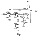
- the short circuit protected circuit illustrated in Figure 6 includes an output stage having series connected transistors MN11 and MN10.
- the circuit output OUT is connected to the point 10 between the series connected transistors in the output stage.
- the circuit output IN at 2 is connected to the control electrodes of both transistors MP3 and MN3 at an input stage.
- the control input of the transistor MN11 is coupled directly to the output of the input stage at 3.
- a first control stage including the transistors MP4 and MN4, coupled between the control input of the transistor MN10 at 4 and the input stage output at 3.
- the short circuit protector for the transistor MN10 includes: a) a first protective circuit or stage with two series connected transistors MN46 and MN6, b) a first further control stage with two series connected transistors MP5 and MN5.
- the first further control stage output is connected at 5 similarly to the circuit in Figure 5, to the control input of the transistor MN46 and the output stage output at 10 to the control input of the transistor MN6.
- This short circuit protector for the transistor MN10 in the circuit illustrated in Figure 6 is principly of the same implementation and mode of operation as the short circuit protector for the transistor MN10 in the circuit illustrated in Figure 5, and should thus require no further description.
- the short circuit protector for the transistor MN11 in Figure 6 differs from that for the transistors MP10 and MN10 in figures 5 and 6, and principly solely comprises a series resistor R coupled between the high feed voltage VDD and the transistor MN11. It will be understood at once by one skilled in the art that a series resistor with sufficiently high resistance coupled in such a manner can restrict the current through the transistor MN11. The greater the resistance, the less will be the short circuit current. However, the possible normal output level and the output current at high potential at the output stage output will be lower and lower the higher and higher the resistance is of the series resistor R. An upper limit for the resistance of it is given by the transistor MN11 not beginning to operate in its linear range when it conducts.
- a suitable resistance for R is therefore determined by the feed voltage VDD and VSS the dimensioning of the transistors MN10 and MN11, as well as the desired ranges of output voltages and output currents at the output stage output during normal operation, i.e. without short circuiting or too low ohmic load.
- the implementation of the short circuit protectors for the transistors MN10 and MP10 should be carried out so that they do not disturb, or at least only insignificantly disturb the normal function of the circuit.
- the short circuit protectors should thus not come into operation unnecessarily, and their action should cease when it is no longer needed, e.g. because the short circuit state has ceased.
- the short circuit protector for the transistor MN10 In order that, for example, the short circuit protector for the transistor MN10 will not come into operation in normal operation in conjunction with the input signal to the circuit at 2 going from low to high level, the potential at the output stage output at 10 must be low before the potential on the stage output from the first further control stage at 5 becomes high. In this way, due to the switchover, both MN46 and MN6 namely cannot be temporarily conductive simultaneously. If instead, the potential at 5 manages to become high before the potential on the output at 10 manages to become low, then both MN46 and MN6 become conductive for a short time, which lowers the potential on the control input at 4 of the transistor MN10, whereby the changeover on the output stage output from high to low potential is delayed.
- the changeover from low to high potential at 5 should thus be comparatively slow or intentionally delayed.
- this can be accomplished for example, by suitable dimensioning of the transistor MP5, which can be achieved by making its width sufficiently small in relation to its length.
- the transistor MN5 shall be dimensioned for analoguous reasons, so that the switchover from high to low level at 5 takes place rapidly, since the potential at 5 must manage to become low before the potential at 10 is allowed to become high.
- the changeover from high to low potential at 8 should be comparatively slow or intentionally delayed in a corresponding way, which similarly can be achieved by making the width of the transistor MN8 sufficiently small in relation to its length.
- the transistor MP8 In order that the short circuit protector for the transistor MP10 in Figure 5 shall not come into operation in conjunction with the input signal to the circuit at 2 changing over from low to high level, the transistor MP8 must be dimensioned analogously with MN5.
- the generally applicable condition is that the respective control stage and further control stage should be implemented so that the changes in potential on the respective stage output, which will be the result of changes of the potential of the input signal on the circuit input, occur earlier or later on the output of a control stage than on the output of the corresponding further control stage, in response to the change in direction of the input signal potential.
- the circuit should return to normal operation when the short circuit to the high feed voltage ceases, or the load returns to permitted values.
- the transistor MN10 must be able to drive the circuit output to low potential within the framework of permitted loading, and with the control signal at 4 still at a lowered potential. This means that their is a minimum permitted potential at 4 in conjunction with short circuiting, and thus a maximum permitted driving capacity of the combination of transistors MN46 and MN6.
- the circuit in Figure 5 should return to normal function after the short circuit protector for the transistor MP10 in Figure 5 has come into operation when the short circuit to the low feed voltage, e.g. VSS ceases or the load returns to permitted values.
- the transistor MP10 must drive the output of the circuit at 10 to high potential within the framework for permitted loading, and with the control signal at 7 still at an increased potential. This means that there is a maximum permitted potential at 7 in conjunction with short circuiting, and thus a maximum permitted driving capacity of the combination of transistors MP9 and MP79.
- the invention is not limited to the two embodiment in Figures 5 and 6, but other embodiments are conceivable with respective components implemented either in MOS or bipolar technique, or in a combination of both.
- the invention is not limited to integrated circuits, even though these are the most natural field of application. It is even conceivable to apply the invention in connection with certain components with controllable conductive capacity other than transistors. Neither the input stage nor the control stages need necessarily completely agree in both embodiment and number with what is illustrated in Figures 5 and 6.
- the feed voltages VDD and VSS shall of course be different but it is not absolutely necessary that one is positive and the other negative, but one of them can have ground potential. The main thing is that in circuits according to Figures 1 - 6, VDD has an appropriately higher potential than VSS.
- control stages shall be implemented and coupled into the circuit so that the changes of potential on the respective stage output, which will be the result of changes of potential in the opposite direction to the above mentioned "given" directions of the input signals on the circuit output, will occur later on a control stage output than on the stage output of a corresponding further control stage.
Landscapes
- Physics & Mathematics (AREA)
- Engineering & Computer Science (AREA)
- Computer Hardware Design (AREA)
- Computing Systems (AREA)
- General Engineering & Computer Science (AREA)
- Mathematical Physics (AREA)
- Amplifiers (AREA)
- Logic Circuits (AREA)
- Emergency Protection Circuit Devices (AREA)
- Protection Of Static Devices (AREA)
- Electronic Switches (AREA)
Applications Claiming Priority (2)
| Application Number | Priority Date | Filing Date | Title |
|---|---|---|---|
| SE8603000 | 1986-07-04 | ||
| SE8603000A SE453784B (sv) | 1986-07-04 | 1986-07-04 | Krets |
Publications (2)
| Publication Number | Publication Date |
|---|---|
| EP0253786A1 true EP0253786A1 (de) | 1988-01-20 |
| EP0253786B1 EP0253786B1 (de) | 1991-03-20 |
Family
ID=20365042
Family Applications (1)
| Application Number | Title | Priority Date | Filing Date |
|---|---|---|---|
| EP87850187A Expired EP0253786B1 (de) | 1986-07-04 | 1987-06-10 | Kurzschlussschutz |
Country Status (4)
| Country | Link |
|---|---|
| US (1) | US4791522A (de) |
| EP (1) | EP0253786B1 (de) |
| DE (1) | DE3768729D1 (de) |
| SE (1) | SE453784B (de) |
Cited By (1)
| Publication number | Priority date | Publication date | Assignee | Title |
|---|---|---|---|---|
| EP0438294A1 (de) * | 1990-01-18 | 1991-07-24 | Honeywell Inc. | Von einem Mikroprozessor gesteuerter statischer Eingangsschutz |
Families Citing this family (4)
| Publication number | Priority date | Publication date | Assignee | Title |
|---|---|---|---|---|
| US5192901A (en) * | 1990-03-16 | 1993-03-09 | Cherry Semiconductor Corporation | Short circuit protection |
| US5256914A (en) * | 1991-10-03 | 1993-10-26 | National Semiconductor Corporation | Short circuit protection circuit and method for output buffers |
| US7369385B2 (en) * | 2002-07-09 | 2008-05-06 | Analog Devices, Inc. | Overload limiting circuit |
| TWI429160B (zh) * | 2010-12-24 | 2014-03-01 | Hanergy Technologies Inc | 保護電路及其保護方法 |
Citations (8)
| Publication number | Priority date | Publication date | Assignee | Title |
|---|---|---|---|---|
| US3447035A (en) * | 1966-07-28 | 1969-05-27 | Westinghouse Electric Corp | Circuitry for protecting a push-pull switching driver stage upon occurrence of a short circuit at the output thereof |
| US3648071A (en) * | 1970-02-04 | 1972-03-07 | Nat Semiconductor Corp | High-speed mos sense amplifier |
| US3749936A (en) * | 1971-08-19 | 1973-07-31 | Texas Instruments Inc | Fault protected output buffer |
| US3786364A (en) * | 1968-09-27 | 1974-01-15 | Rca Corp | Semiconductor amplifier protection |
| DE2947062A1 (de) * | 1978-11-24 | 1980-06-04 | Novanex Automation Nv | Anordnung zum schutz gegen ueberlastung oder kurzschluss eines audioverstaerkers |
| EP0083504A1 (de) * | 1981-12-29 | 1983-07-13 | Fujitsu Limited | MOS-Ausgangstreiberschaltung |
| DE3103852C2 (de) * | 1980-02-08 | 1983-09-22 | Tokyo Shibaura Denki K.K., Kawasaki, Kanagawa | Leistungsverstärker |
| EP0091203A1 (de) * | 1982-04-02 | 1983-10-12 | Ampex Corporation | Überlastungsschutzeinrichtung |
Family Cites Families (8)
| Publication number | Priority date | Publication date | Assignee | Title |
|---|---|---|---|---|
| US4020395A (en) * | 1975-09-17 | 1977-04-26 | The United States Of America As Represented By The Secretary Of The Army | Transient voltage protection circuit for a DC power supply |
| JPS55178A (en) * | 1979-03-10 | 1980-01-05 | Tokyo Juki Industrial Co Ltd | Controller of button installing device |
| IT1211141B (it) * | 1981-12-04 | 1989-09-29 | Ates Componenti Elettron | Circuito limitatore-trasduttore disegnali in alternata codificati in forma binaria, come stadio d'ingresso di un circuito integrato a igfet. |
| US4495536A (en) * | 1982-12-27 | 1985-01-22 | Motorola, Inc. | Voltage transient protection circuit |
| JPS59208942A (ja) * | 1983-05-13 | 1984-11-27 | Nec Corp | 半導体回路 |
| GB8321549D0 (en) * | 1983-08-10 | 1983-09-14 | British Telecomm | Electronic switch |
| US4581672A (en) * | 1983-08-31 | 1986-04-08 | National Semiconductor Corporation | Internal high voltage (Vpp) regulator for integrated circuits |
| US4706159A (en) * | 1985-03-12 | 1987-11-10 | Pitney Bowes Inc. | Multiple power supply overcurrent protection circuit |
-
1986
- 1986-07-04 SE SE8603000A patent/SE453784B/sv not_active IP Right Cessation
-
1987
- 1987-06-10 EP EP87850187A patent/EP0253786B1/de not_active Expired
- 1987-06-10 DE DE8787850187T patent/DE3768729D1/de not_active Expired - Lifetime
- 1987-06-23 US US07/065,393 patent/US4791522A/en not_active Expired - Lifetime
Patent Citations (8)
| Publication number | Priority date | Publication date | Assignee | Title |
|---|---|---|---|---|
| US3447035A (en) * | 1966-07-28 | 1969-05-27 | Westinghouse Electric Corp | Circuitry for protecting a push-pull switching driver stage upon occurrence of a short circuit at the output thereof |
| US3786364A (en) * | 1968-09-27 | 1974-01-15 | Rca Corp | Semiconductor amplifier protection |
| US3648071A (en) * | 1970-02-04 | 1972-03-07 | Nat Semiconductor Corp | High-speed mos sense amplifier |
| US3749936A (en) * | 1971-08-19 | 1973-07-31 | Texas Instruments Inc | Fault protected output buffer |
| DE2947062A1 (de) * | 1978-11-24 | 1980-06-04 | Novanex Automation Nv | Anordnung zum schutz gegen ueberlastung oder kurzschluss eines audioverstaerkers |
| DE3103852C2 (de) * | 1980-02-08 | 1983-09-22 | Tokyo Shibaura Denki K.K., Kawasaki, Kanagawa | Leistungsverstärker |
| EP0083504A1 (de) * | 1981-12-29 | 1983-07-13 | Fujitsu Limited | MOS-Ausgangstreiberschaltung |
| EP0091203A1 (de) * | 1982-04-02 | 1983-10-12 | Ampex Corporation | Überlastungsschutzeinrichtung |
Cited By (1)
| Publication number | Priority date | Publication date | Assignee | Title |
|---|---|---|---|---|
| EP0438294A1 (de) * | 1990-01-18 | 1991-07-24 | Honeywell Inc. | Von einem Mikroprozessor gesteuerter statischer Eingangsschutz |
Also Published As
| Publication number | Publication date |
|---|---|
| SE8603000L (sv) | 1988-01-05 |
| US4791522A (en) | 1988-12-13 |
| SE453784B (sv) | 1988-02-29 |
| DE3768729D1 (de) | 1991-04-25 |
| EP0253786B1 (de) | 1991-03-20 |
| SE8603000D0 (sv) | 1986-07-04 |
Similar Documents
| Publication | Publication Date | Title |
|---|---|---|
| US5945816A (en) | Self-biased power isolator system | |
| EP0476365A1 (de) | Adaptive Vorspannungsstromsteuerungsschaltung | |
| KR100360325B1 (ko) | 출력제어장치 | |
| US7609498B2 (en) | Inverted circuit overcurrent protection device and hybrid integrated circuit device with the same incorporated | |
| EP0346011B1 (de) | Verstärker | |
| JPH02166915A (ja) | 負荷反応遷移制御付バツフア回路 | |
| US6353521B1 (en) | Device and method for protecting an integrated circuit during an ESD event | |
| EP0473840A1 (de) | Puffer mit gesteuerter Anstiegszeit | |
| CN110785933B (zh) | 半导体开关元件的短路保护电路 | |
| EP0253786B1 (de) | Kurzschlussschutz | |
| US6169420B1 (en) | Output buffer | |
| US5500610A (en) | Very high current integrated circuit output buffer with short circuit protection and reduced power bus spikes | |
| JPH02305007A (ja) | 増幅器 | |
| US3441864A (en) | Transistor amplifier protective circuits | |
| EP0130079B1 (de) | MOS-Ausgangspuffer für grosse Stromstärke | |
| US4229706A (en) | Audio amplifier | |
| JP2007534244A (ja) | 出力段システム | |
| US7049890B2 (en) | Operational amplifier with self control circuit for realizing high slew rate throughout full operating range | |
| US4488064A (en) | Integrated circuit with a common power supply for silicon and gallium arsenide circuit portions | |
| JP2001177387A (ja) | 負荷駆動装置 | |
| US6414515B1 (en) | Failsafe interface circuit with extended drain devices | |
| KR101621973B1 (ko) | 주행안전제어시스템의 엔진 컨트롤 유닛 모터 또는 fet의 단락시의 보호회로. | |
| US4910477A (en) | Bridge-type linear amplifier with wide dynamic range and high efficiency | |
| EP0406967B1 (de) | Verstärkerschaltung | |
| JPH07112133B2 (ja) | 線形増幅器 |
Legal Events
| Date | Code | Title | Description |
|---|---|---|---|
| PUAI | Public reference made under article 153(3) epc to a published international application that has entered the european phase |
Free format text: ORIGINAL CODE: 0009012 |
|
| AK | Designated contracting states |
Kind code of ref document: A1 Designated state(s): BE DE GB NL |
|
| 17P | Request for examination filed |
Effective date: 19880325 |
|
| 17Q | First examination report despatched |
Effective date: 19900820 |
|
| GRAA | (expected) grant |
Free format text: ORIGINAL CODE: 0009210 |
|
| AK | Designated contracting states |
Kind code of ref document: B1 Designated state(s): BE DE GB NL |
|
| REF | Corresponds to: |
Ref document number: 3768729 Country of ref document: DE Date of ref document: 19910425 |
|
| PLBE | No opposition filed within time limit |
Free format text: ORIGINAL CODE: 0009261 |
|
| STAA | Information on the status of an ep patent application or granted ep patent |
Free format text: STATUS: NO OPPOSITION FILED WITHIN TIME LIMIT |
|
| 26N | No opposition filed | ||
| PGFP | Annual fee paid to national office [announced via postgrant information from national office to epo] |
Ref country code: BE Payment date: 19990614 Year of fee payment: 13 |
|
| PGFP | Annual fee paid to national office [announced via postgrant information from national office to epo] |
Ref country code: DE Payment date: 20000518 Year of fee payment: 14 |
|
| PGFP | Annual fee paid to national office [announced via postgrant information from national office to epo] |
Ref country code: GB Payment date: 20000519 Year of fee payment: 14 |
|
| PGFP | Annual fee paid to national office [announced via postgrant information from national office to epo] |
Ref country code: NL Payment date: 20000524 Year of fee payment: 14 |
|
| PG25 | Lapsed in a contracting state [announced via postgrant information from national office to epo] |
Ref country code: BE Free format text: LAPSE BECAUSE OF NON-PAYMENT OF DUE FEES Effective date: 20000630 |
|
| BERE | Be: lapsed |
Owner name: TELEFONAKTIEBOLAGET L M ERICSSON Effective date: 20000630 |
|
| PG25 | Lapsed in a contracting state [announced via postgrant information from national office to epo] |
Ref country code: GB Free format text: LAPSE BECAUSE OF NON-PAYMENT OF DUE FEES Effective date: 20010610 |
|
| PG25 | Lapsed in a contracting state [announced via postgrant information from national office to epo] |
Ref country code: NL Free format text: LAPSE BECAUSE OF NON-PAYMENT OF DUE FEES Effective date: 20020101 |
|
| GBPC | Gb: european patent ceased through non-payment of renewal fee |
Effective date: 20010610 |
|
| NLV4 | Nl: lapsed or anulled due to non-payment of the annual fee |
Effective date: 20020101 |
|
| PG25 | Lapsed in a contracting state [announced via postgrant information from national office to epo] |
Ref country code: DE Free format text: LAPSE BECAUSE OF NON-PAYMENT OF DUE FEES Effective date: 20020403 |