EP0254406B1 - Circuit de commutation pour signaux d'horloge - Google Patents
Circuit de commutation pour signaux d'horloge Download PDFInfo
- Publication number
- EP0254406B1 EP0254406B1 EP87304895A EP87304895A EP0254406B1 EP 0254406 B1 EP0254406 B1 EP 0254406B1 EP 87304895 A EP87304895 A EP 87304895A EP 87304895 A EP87304895 A EP 87304895A EP 0254406 B1 EP0254406 B1 EP 0254406B1
- Authority
- EP
- European Patent Office
- Prior art keywords
- flip
- clock signal
- clock
- flops
- selection means
- Prior art date
- Legal status (The legal status is an assumption and is not a legal conclusion. Google has not performed a legal analysis and makes no representation as to the accuracy of the status listed.)
- Expired
Links
- 238000001514 detection method Methods 0.000 claims 1
- 238000010586 diagram Methods 0.000 description 1
Images
Classifications
-
- G—PHYSICS
- G04—HOROLOGY
- G04G—ELECTRONIC TIME-PIECES
- G04G3/00—Producing timing pulses
-
- H—ELECTRICITY
- H04—ELECTRIC COMMUNICATION TECHNIQUE
- H04L—TRANSMISSION OF DIGITAL INFORMATION, e.g. TELEGRAPHIC COMMUNICATION
- H04L7/00—Arrangements for synchronising receiver with transmitter
- H04L7/0079—Receiver details
- H04L7/0083—Receiver details taking measures against momentary loss of synchronisation, e.g. inhibiting the synchronisation, using idle words or using redundant clocks
Definitions
- This invention relates to a switching circuit for selecting between two clock signals.
- the system may include a programmable clock source, which has an undefined output while it is being programmed.
- a programmable clock source which has an undefined output while it is being programmed.
- the object of the invention is to overcome this problem.
- US-A-4229699 discloses a switching circuit for selecting between first and second clock signals, comprising first selection means for selecting the first clock signal, second selection means for selecting the second clock signal, and control means operable to disable the first selection means in synchronism with the first clock signal and then, after a predetermined time delay, to enable the second selection means in synchronism with the second clock signal.
- such a switching circuit for selecting between first and second clock signals is characterised in that the control means comprises a chain of flip-flops connected in series, the first flip-flop in the series receiving a selection control signal specifying which of the clock signals is to be selected, wherein the chain of flip-flops comprises first, second and third sections, the first section and third section being clocked by the first clock signal and the second section being clocked by the second clock signal, wherein the output of the first and third section are combined in a logic gate to produce a first control signal which enables the first selection means when both those outputs have a predetermined value, and wherein the output of the second section provides a second control signal which enables the second selection means when that output has a predetermined value.
- the first clock is deselected in synchronism with that clock, and then, after a period in which neither clock is selected, the second clock is selected in synchronism with that second clock. This avoids the risk of undesired short clock pulses.
- the switching circuit can also operate in a similar manner for switching from the second signal to the first.
- the control means is alternatively operable to disable the second selection means in synchronism with the second clock signal and then, after a predetermined time delay, to enable the first selection means in synchronism with the first clock signal.
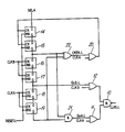
- this shows a switching circuit for selecting between two input clock signals CLKA and CLKB.
- the selected clock signal appears, in inverted form, as output clock signal CLKS.L.
- the output clock signal CLKS.L is produced by a NAND gate 10 having two inputs.
- One input of the NAND gate is connected to the output of an OR gate 11, one input of which receives the clock signal CLKA and the other input of which receives a control signal GOA.L for selecting CLKA.
- the "L" indicates that the low voltage logic level is the active level for this signal GOA.L.
- the other input of the NAND gate 10 is connected to the output of an OR gate 12, one input of which receives the clock signal CLKB and the other input of which receives a control signal GOB.L for selecting CLKB.
- the switching circuit is controlled by a chain of six D-type flip-flops (bistable circuits) 14-19. Each of these flip-flops has a data input D, a data output Q, a clock input CK, and a reset input MR. The Q output of each of the flip-flops, other than the last, is connected to the D input of the next in the chain.
- the D input of the first flip-flop 14 receives a selection control signal SELA which indicates which of the clock signals is to be selected.
- SELA selection control signal
- the clock inputs CK of flip-flops 14, 15 are both connected to the output of an OR gate 20, one input of which receives the clock signal CLKA and the other input of which receives a control signal CKEN.L.
- CKEN.L when CKEN.L is low, the flip-flops 14, 15 are both clocked at each beat of the clock signal CLKA.
- CKEN.L When CKEN.L is high, the output of the OR gate 20 is held at a constant high level and so the flip-flops 14, 15 are not clocked.
- the clock inputs CK of flip-flops 16, 17 both receive the clock signal CLKB, while the clock inputs of flip-flops 18, 19 both receive the clock signal CLKA.
- the reset inputs MR of all six flip-flops receive a reset signal RESET.L which resets each flip-flop to the state in which the Q output is low.
- the Q output of flip-flop 17 provides the control signal GOB.L which selects the clock CLKB.
- the Q outputs of flip-flops 15 and 19 are combined in a NAND gate 21, the output of which provides the control signal GOA.L which selects the clock signal CLKA.
- the Q outputs of these two flip-flops 15, 19 are also combined in an EXCLUSIVE-OR gate 22, the output of which provides the signal CKEN.L which permits the clock CLKA to be applied to the flip-flops 14, 15.
- flip-flop 14 At the first beat of clock CLKA, flip-flop 14 is set, so that its Q output goes high.
- flip-flop 15 is set, so that its Q output goes high.
- the flip-flop 18 At the first beat of clock CLKA following the setting of flip-flop 17, the flip-flop 18 is set and then, at the next beat of CLKA, the flip-flop 19 is also set.
- flip-flop 14 At the first beat of CLKA, flip-flop 14 is reset, and then at the next beat of CLKA flip-flop 15 is also reset.
- the Q output of flip-flop 15 is therefore now low. This causes the signal CKEN.L to go high, preventing further clocking of the flip-flops 14, 15.
- the low output of flip-flop 15 also disables the NAND gate 21, making GOA.L high, which de-selects the clock CLKA.
- flip-flop 16 At the first beat of CLKB following resetting of flip-flop 15, flip-flop 16 is reset and then, at the next beat of CLKB, flip-flop 17 is also reset. This makes GOB.L low, which selects the clock CLKB.
Landscapes
- Physics & Mathematics (AREA)
- General Physics & Mathematics (AREA)
- Engineering & Computer Science (AREA)
- Computer Networks & Wireless Communication (AREA)
- Signal Processing (AREA)
- Shift Register Type Memory (AREA)
- Liquid Crystal Display Device Control (AREA)
- Manipulation Of Pulses (AREA)
- Electronic Switches (AREA)
Claims (4)
Applications Claiming Priority (2)
| Application Number | Priority Date | Filing Date | Title |
|---|---|---|---|
| GB8615399 | 1986-06-24 | ||
| GB868615399A GB8615399D0 (en) | 1986-06-24 | 1986-06-24 | Switching circuit |
Publications (3)
| Publication Number | Publication Date |
|---|---|
| EP0254406A2 EP0254406A2 (fr) | 1988-01-27 |
| EP0254406A3 EP0254406A3 (en) | 1989-04-26 |
| EP0254406B1 true EP0254406B1 (fr) | 1991-01-09 |
Family
ID=10600007
Family Applications (1)
| Application Number | Title | Priority Date | Filing Date |
|---|---|---|---|
| EP87304895A Expired EP0254406B1 (fr) | 1986-06-24 | 1987-06-03 | Circuit de commutation pour signaux d'horloge |
Country Status (5)
| Country | Link |
|---|---|
| US (1) | US4855615A (fr) |
| EP (1) | EP0254406B1 (fr) |
| JP (1) | JPS635616A (fr) |
| DE (1) | DE3767243D1 (fr) |
| GB (1) | GB8615399D0 (fr) |
Families Citing this family (31)
| Publication number | Priority date | Publication date | Assignee | Title |
|---|---|---|---|---|
| JP2643146B2 (ja) * | 1987-05-14 | 1997-08-20 | ソニー株式会社 | マイクロコンピュータのクロック生成回路 |
| JP2739964B2 (ja) * | 1988-09-28 | 1998-04-15 | 株式会社東芝 | クロック切替回路 |
| US5123107A (en) * | 1989-06-20 | 1992-06-16 | Mensch Jr William D | Topography of CMOS microcomputer integrated circuit chip including core processor and memory, priority, and I/O interface circuitry coupled thereto |
| JP2591201B2 (ja) * | 1989-12-21 | 1997-03-19 | 日本モトローラ株式会社 | 信号切替装置 |
| FR2661297B1 (fr) * | 1990-04-18 | 1993-02-12 | Alcatel Radiotelephone | Circuit de multiplexage de signaux d'horloge. |
| US5120990A (en) * | 1990-06-29 | 1992-06-09 | Analog Devices, Inc. | Apparatus for generating multiple phase clock signals and phase detector therefor |
| JPH04288607A (ja) * | 1991-03-18 | 1992-10-13 | Sharp Corp | クロック信号切り換え回路 |
| EP0533992A1 (fr) * | 1991-09-27 | 1993-03-31 | Siemens Nixdorf Informationssysteme Aktiengesellschaft | Méthode et dispositif pour accomplir des transmissions de données synchrones |
| US5274678A (en) * | 1991-12-30 | 1993-12-28 | Intel Corporation | Clock switching apparatus and method for computer systems |
| US5388241A (en) * | 1992-03-10 | 1995-02-07 | Northrop Grumman Corporation | Asynchronous circuit for 2-cycle to 4-cycle handshake conversion |
| JPH05268205A (ja) * | 1992-03-19 | 1993-10-15 | Fujitsu Ltd | クロック切換え回路 |
| US5254888A (en) * | 1992-03-27 | 1993-10-19 | Picopower Technology Inc. | Switchable clock circuit for microprocessors to thereby save power |
| US5327019A (en) * | 1992-07-30 | 1994-07-05 | Alcatel Network Systems, Inc. | Double edge single data flip-flop circuitry |
| US5726593A (en) * | 1992-10-27 | 1998-03-10 | Nokia Telecommunications Oy | Method and circuit for switching between a pair of asynchronous clock signals |
| FI91471C (fi) * | 1992-10-27 | 1994-06-27 | Nokia Telecommunications Oy | Menetelmä ja laite asynkronisten kellosignaalien vaihtokytkemiseksi |
| US5315181A (en) * | 1993-07-07 | 1994-05-24 | Maxtor Corporation | Circuit for synchronous, glitch-free clock switching |
| US5587675A (en) * | 1993-08-12 | 1996-12-24 | At&T Global Information Solutions Company | Multiclock controller |
| US5572554A (en) * | 1994-07-29 | 1996-11-05 | Loral Corporation | Synchronizer and method therefor |
| US5604452A (en) * | 1995-04-03 | 1997-02-18 | Exar Corporation | Clock generator using a state machine to switch between two offset clocks |
| US5793233A (en) * | 1996-05-30 | 1998-08-11 | Sun Microsystems, Inc. | Apparatus and method for generating a phase detection signal that coordinates the phases of separate clock signals |
| US5811995A (en) * | 1996-08-02 | 1998-09-22 | Advanced Micro Devices, Inc. | Circuit for switching between different frequency clock domains that are out of phase |
| US5859553A (en) * | 1997-01-08 | 1999-01-12 | Microchip Technology Incorporated | System and method for a glitchless transition between differing delay paths |
| DE19844671C1 (de) * | 1998-09-29 | 1999-10-07 | Siemens Ag | Spikefreie Taktumschaltung |
| US6453425B1 (en) | 1999-11-23 | 2002-09-17 | Lsi Logic Corporation | Method and apparatus for switching clocks presented to synchronous SRAMs |
| US6323715B1 (en) | 1999-12-30 | 2001-11-27 | Koninklijke Philips Electronics N.V. (Kpeuv) | Method and apparatus for selecting a clock signal without producing a glitch |
| US6982573B2 (en) * | 2001-05-30 | 2006-01-03 | Stmicroelectronics Limited | Switchable clock source |
| EP1263139A3 (fr) * | 2001-05-30 | 2006-07-05 | STMicroelectronics Limited | Multiplexeur sans signaux transitoires |
| US6774681B2 (en) | 2001-05-30 | 2004-08-10 | Stmicroelectronics Limited | Switchable clock source |
| US7961820B2 (en) * | 2004-01-29 | 2011-06-14 | Nxp B.V. | Programmable and pausable clock generation unit |
| US7629828B1 (en) * | 2007-04-27 | 2009-12-08 | Zilog, Inc. | Glitch-free clock multiplexer that provides an output clock signal based on edge detection |
| CN105406984B (zh) * | 2015-10-22 | 2019-05-31 | 上海斐讯数据通信技术有限公司 | 一种实现主备倒换背板时钟的系统及方法 |
Family Cites Families (10)
| Publication number | Priority date | Publication date | Assignee | Title |
|---|---|---|---|---|
| JPS4925060B1 (fr) * | 1969-04-08 | 1974-06-27 | ||
| US3751679A (en) * | 1971-03-04 | 1973-08-07 | Honeywell Inc | Fail-safe monitoring apparatus |
| US4201927A (en) * | 1977-05-24 | 1980-05-06 | Rca Corporation | Circuit for producing sequentially spaced pulses |
| US4229699A (en) * | 1978-05-22 | 1980-10-21 | Data General Corporation | Multiple clock selection system |
| DE2907170C3 (de) * | 1979-02-23 | 1981-08-20 | Siemens AG, 1000 Berlin und 8000 München | Taktgenerator mit umschaltbarer Taktfrequenz für eine datenverarbeitende Anlage |
| FR2506478A1 (fr) * | 1981-05-20 | 1982-11-26 | Telephonie Ind Commerciale | Dispositif pour augmenter la securite de fonctionnement d'une horloge dupliquee |
| US4677433A (en) * | 1983-02-16 | 1987-06-30 | Daisy Systems Corporation | Two-speed clock scheme for co-processors |
| US4696019A (en) * | 1984-09-19 | 1987-09-22 | United Technologies Corporation | Multi-channel clock synchronizer |
| US4689496A (en) * | 1985-03-27 | 1987-08-25 | Ncr Corporation | Two clock boot circuit |
| US4644568A (en) * | 1985-03-28 | 1987-02-17 | At&T Bell Laboratories | Timing signal distribution arrangement |
-
1986
- 1986-06-24 GB GB868615399A patent/GB8615399D0/en active Pending
-
1987
- 1987-06-03 DE DE8787304895T patent/DE3767243D1/de not_active Expired - Fee Related
- 1987-06-03 EP EP87304895A patent/EP0254406B1/fr not_active Expired
- 1987-06-12 US US07/062,158 patent/US4855615A/en not_active Expired - Fee Related
- 1987-06-24 JP JP62155615A patent/JPS635616A/ja active Pending
Also Published As
| Publication number | Publication date |
|---|---|
| DE3767243D1 (de) | 1991-02-14 |
| GB8615399D0 (en) | 1986-07-30 |
| EP0254406A3 (en) | 1989-04-26 |
| EP0254406A2 (fr) | 1988-01-27 |
| US4855615A (en) | 1989-08-08 |
| JPS635616A (ja) | 1988-01-11 |
Similar Documents
| Publication | Publication Date | Title |
|---|---|---|
| EP0254406B1 (fr) | Circuit de commutation pour signaux d'horloge | |
| US4853653A (en) | Multiple input clock selector | |
| US5731715A (en) | Glitch-free clock enable circuit | |
| US4970405A (en) | Clock selection circuit for selecting one of a plurality of clock pulse signals | |
| US5261081A (en) | Sequence control apparatus for producing output signals in synchronous with a consistent delay from rising or falling edge of clock input signal | |
| US6320436B1 (en) | Clock skew removal apparatus | |
| US4538272A (en) | Prioritized clock selection circuit | |
| US5502409A (en) | Clock switcher circuit | |
| EP0131233B1 (fr) | Générateur à grande vitesse, programmable, de signaux temporels | |
| US7180336B2 (en) | Glitch-free clock switching apparatus | |
| US5422918A (en) | Clock phase detecting system for detecting the phase difference between two clock phases regardless of which of the two clock phases leads the other | |
| WO1999026341A1 (fr) | Circuit electronique a bascule a double front raide | |
| WO2021180230A1 (fr) | Circuit de commutation d'horloge sans bruit parasite | |
| US6348828B1 (en) | Clock enable circuit for use in a high speed reprogrammable delay line incorporating glitchless enable/disable functionality | |
| US4955040A (en) | Method and apparatus for generating a correction signal in a digital clock recovery device | |
| US5327076A (en) | Glitchless test signal generator | |
| JPH1198007A (ja) | 分周回路 | |
| US4801813A (en) | Event distribution and combination system | |
| US4759042A (en) | Parallel-to-serial converter | |
| JP3219141B2 (ja) | クロック切替回路 | |
| KR100238208B1 (ko) | 동기식 직렬 입출력 회로 | |
| GB2214314A (en) | Automatic circuit tester | |
| JPH0450657Y2 (fr) | ||
| KR19980050372A (ko) | 데이타 전송 동기용 클럭 발생장치 | |
| JPS61285523A (ja) | クロツク切換回路 |
Legal Events
| Date | Code | Title | Description |
|---|---|---|---|
| PUAI | Public reference made under article 153(3) epc to a published international application that has entered the european phase |
Free format text: ORIGINAL CODE: 0009012 |
|
| AK | Designated contracting states |
Kind code of ref document: A2 Designated state(s): DE FR GB |
|
| PUAL | Search report despatched |
Free format text: ORIGINAL CODE: 0009013 |
|
| AK | Designated contracting states |
Kind code of ref document: A3 Designated state(s): DE FR GB |
|
| RAP1 | Party data changed (applicant data changed or rights of an application transferred) |
Owner name: AMT(HOLDINGS) LIMITED |
|
| 17P | Request for examination filed |
Effective date: 19891012 |
|
| 17Q | First examination report despatched |
Effective date: 19891211 |
|
| GRAA | (expected) grant |
Free format text: ORIGINAL CODE: 0009210 |
|
| AK | Designated contracting states |
Kind code of ref document: B1 Designated state(s): DE FR GB |
|
| ET | Fr: translation filed | ||
| REF | Corresponds to: |
Ref document number: 3767243 Country of ref document: DE Date of ref document: 19910214 |
|
| PGFP | Annual fee paid to national office [announced via postgrant information from national office to epo] |
Ref country code: GB Payment date: 19910528 Year of fee payment: 5 |
|
| PGFP | Annual fee paid to national office [announced via postgrant information from national office to epo] |
Ref country code: FR Payment date: 19910619 Year of fee payment: 5 |
|
| PGFP | Annual fee paid to national office [announced via postgrant information from national office to epo] |
Ref country code: DE Payment date: 19910628 Year of fee payment: 5 |
|
| PLBE | No opposition filed within time limit |
Free format text: ORIGINAL CODE: 0009261 |
|
| STAA | Information on the status of an ep patent application or granted ep patent |
Free format text: STATUS: NO OPPOSITION FILED WITHIN TIME LIMIT |
|
| 26N | No opposition filed | ||
| PG25 | Lapsed in a contracting state [announced via postgrant information from national office to epo] |
Ref country code: GB Effective date: 19920603 |
|
| GBPC | Gb: european patent ceased through non-payment of renewal fee |
Effective date: 19920603 |
|
| PG25 | Lapsed in a contracting state [announced via postgrant information from national office to epo] |
Ref country code: FR Effective date: 19930226 |
|
| PG25 | Lapsed in a contracting state [announced via postgrant information from national office to epo] |
Ref country code: DE Effective date: 19930302 |
|
| REG | Reference to a national code |
Ref country code: FR Ref legal event code: ST |