EP0254952A2 - Système de bus optique avec un bus de données optique ainsi qu'une partie émettrice et réceptrice pour un tel système - Google Patents
Système de bus optique avec un bus de données optique ainsi qu'une partie émettrice et réceptrice pour un tel système Download PDFInfo
- Publication number
- EP0254952A2 EP0254952A2 EP87110167A EP87110167A EP0254952A2 EP 0254952 A2 EP0254952 A2 EP 0254952A2 EP 87110167 A EP87110167 A EP 87110167A EP 87110167 A EP87110167 A EP 87110167A EP 0254952 A2 EP0254952 A2 EP 0254952A2
- Authority
- EP
- European Patent Office
- Prior art keywords
- bits
- data
- part according
- scrambled
- clock
- Prior art date
- Legal status (The legal status is an assumption and is not a legal conclusion. Google has not performed a legal analysis and makes no representation as to the accuracy of the status listed.)
- Withdrawn
Links
- 230000003287 optical effect Effects 0.000 title claims abstract description 15
- 238000001514 detection method Methods 0.000 claims abstract description 13
- 230000005540 biological transmission Effects 0.000 claims description 7
- 238000011084 recovery Methods 0.000 claims description 7
- 230000001960 triggered effect Effects 0.000 claims description 5
- 230000001360 synchronised effect Effects 0.000 claims description 2
- 239000003550 marker Substances 0.000 claims 5
- 238000012216 screening Methods 0.000 claims 4
- 238000001914 filtration Methods 0.000 claims 1
- 238000007873 sieving Methods 0.000 claims 1
- 238000006243 chemical reaction Methods 0.000 abstract description 4
- 230000005693 optoelectronics Effects 0.000 abstract 1
- 239000000835 fiber Substances 0.000 description 30
- 238000010586 diagram Methods 0.000 description 6
- 239000013307 optical fiber Substances 0.000 description 5
- 230000001934 delay Effects 0.000 description 3
- 230000007704 transition Effects 0.000 description 3
- 241001136792 Alle Species 0.000 description 1
- 238000010521 absorption reaction Methods 0.000 description 1
- 230000003321 amplification Effects 0.000 description 1
- 230000008859 change Effects 0.000 description 1
- 238000004891 communication Methods 0.000 description 1
- 239000012141 concentrate Substances 0.000 description 1
- 230000008878 coupling Effects 0.000 description 1
- 238000010168 coupling process Methods 0.000 description 1
- 238000005859 coupling reaction Methods 0.000 description 1
- 238000011156 evaluation Methods 0.000 description 1
- 238000003384 imaging method Methods 0.000 description 1
- 238000003199 nucleic acid amplification method Methods 0.000 description 1
- 230000005855 radiation Effects 0.000 description 1
- 230000035945 sensitivity Effects 0.000 description 1
- 230000002123 temporal effect Effects 0.000 description 1
Images



Classifications
-
- H—ELECTRICITY
- H04—ELECTRIC COMMUNICATION TECHNIQUE
- H04L—TRANSMISSION OF DIGITAL INFORMATION, e.g. TELEGRAPHIC COMMUNICATION
- H04L25/00—Baseband systems
- H04L25/02—Details ; arrangements for supplying electrical power along data transmission lines
- H04L25/03—Shaping networks in transmitter or receiver, e.g. adaptive shaping networks
- H04L25/03828—Arrangements for spectral shaping; Arrangements for providing signals with specified spectral properties
- H04L25/03866—Arrangements for spectral shaping; Arrangements for providing signals with specified spectral properties using scrambling
-
- H—ELECTRICITY
- H04—ELECTRIC COMMUNICATION TECHNIQUE
- H04L—TRANSMISSION OF DIGITAL INFORMATION, e.g. TELEGRAPHIC COMMUNICATION
- H04L12/00—Data switching networks
- H04L12/28—Data switching networks characterised by path configuration, e.g. LAN [Local Area Networks] or WAN [Wide Area Networks]
- H04L12/44—Star or tree networks
Definitions
- the present invention relates to an optical bus system with an optical data bus according to the preamble of claim 1 and a transmitter and receiver part for such a system.
- the bus system according to the invention is suitable for communication systems.
- the subscribers are connected to the active star coupler via optical fibers.
- the transmission-side fibers of the subscribers couple to an input-side optical fiber bundle.
- the fibers are fused into a rod at one end of this optical fiber bundle.
- the end face of this rod can be applied to the light-sensitive surface S of a detector or a plurality of detectors, for example a PIN diode or APD are mapped, which convert the supplied optical signals into electrical signals.
- the amplified electrical signal passes through a clamp circuit which ensures that the signals with a constant level shift as little as possible in terms of potential.
- the electrical signals then arrive at E in the collision detection circuit shown in Figure 2, which detects the collisions, i.e. recognizes the superposition of at least two bit streams and generates a JAM signal in the event of such a collision.
- a JAM signal is a bit pattern that does not appear in the scrambled bit pattern of the data and can therefore be recognized as a collision signal.
- the electrical data from A is optically converted and fed to the participants' receivers via the optical fibers.
- the collision detection circuit At the input of the collision detection circuit according to FIG. 2 there are two threshold value comparators, to which the electrical signals are fed via E.
- the threshold values of the two comparators are dimensioned such that the comparator K2 only emits a signal if at least two signals are superimposed.
- the comparator K1 on the other hand, already responds when signals arrive from only one participant.
- the transmission error detection circuit ÜE which is framed by dash-dotted lines, is provided.
- Such a circuit has already been proposed in the earlier patent application P 32 24 664.1 (VPA 82 P 1509) and its mode of operation is also described there (see there in particular FIG. 3 and associated description).
- the circuit ÜE exists essentially of a shift register SR4 connected to the comparator K2, a monostable multivibrator M.4 and an AND gate.
- the clock for operating the shift register SR4 is supplied by a clock recovery circuit TR1, which recovers the clock from the signals supplied by the participants.
- the output Z11 of the second existing AND gate is set to the binary value '0' and on an output line Z8 or Z12 of a monostable multivibrator M6 or an OR gate, the JAM signal appears for example, an uninterrupted sequence of bits of the binary value '1', corresponding to the time constant of the monostable multi-vibrator M5 in Figure 2. This time constant is chosen approximately equal to the round trip time of the signals through the bus route.
- the JAM signal is chosen to be longer than any uninterrupted sequence of bits of either one or the other binary value occurring among the scrambled data signals.
- the optical-electrical converter of the active coupler In the optical-electrical converter of the active coupler according to FIG. 1, one wants to get by with as few detectors as possible.
- the aim here is to estimate how many fiber end faces can simultaneously direct their light onto a given detector area. It is assumed that M fibers are fused at one end to form a cylindrical rod, so that the end face F B of the rod with the diameter 0 ⁇ B is equal to the sum of the M fiber end faces.
- the diameter 0 ⁇ E of the single fiber for example, 140 ⁇ m and the light-sensitive surface of the detector is 1 mm2
- all light from the end face of a rectangular rod for example, which is made of 51 fused fibers, reaches the detector if the detector is immediately in front of the Rod end face is butt coupled.
- This behavior is independent of the numerical aperture of the fibers. If you want to concentrate the light from several fibers on a detector, the rod end area, which is larger than 1 mm2, is reduced to the detector using optics, for example map. Depending on the number and numerical aperture of the fibers and the complexity of the optics, additional detectors may have to be added.
- the electrical TTL signals occurring at A are converted back into optical pulses by the electrical-optical converter, for example a light-emitting diode (LED) or a laser diode (LD).
- the electrical-optical converter for example a light-emitting diode (LED) or a laser diode (LD).
- the number of converters required for this essentially depends on the type of converter and the number of participants. It should be shown that an LED in the active coupler is required for about 500 participants when using, for example, Burrus LEDs in the system: It is assumed that, for example, 100 ⁇ W can be coupled into a step profile fiber by a butt coupling from an LED. However, the total radiated power of a Burrus LED at a light wavelength ⁇ of 850 nm is at least 5 mW.
- the beam angle of the transducer is reduced by an optical system, which for an LED is approximately ⁇ 60 °, until the angle of the fibers corresponding to the numerical aperture of a fiber is reached.
- the image of the radiating surface of the transducer is of course larger than the radiating surface of the transducer.
- the cross section F ⁇ B of the LED area shown is not greater than 0.77 mm2.
- F B is still less than 0.04 mm.
- the active star coupler On the transmitting and receiving side of the active star coupler, it is also possible, if necessary, to dispense with imaging optics.
- the M fibers of the bundle are fused at one end and taped or tapered so that the cross section of the rod is reduced.
- the end face of the rod On the receiving side of the coupler, the end face of the rod is selected to be at most equal to the detector face and this end face is positioned directly in front of the detector face.
- the taper or taper may only be so steep that the rays neither run back into themselves nor emerge into the surrounding area.
- the taper of the rod should be designed so that the angles when the fibers of the optical fiber bundle transition to the system fibers leading to the participants the light rays have become flat enough so that the rays are guided in the system fibers.
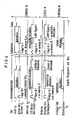
- the length of the header bits is determined by the clock recovery circuit in the receiver section (see Figures 5a and 5b).
- the clock s8 is always on the scrambler.
- Q becomes equal to '0' from the monostable multivibrator M.2, which is triggered by the trailing edge of the valid signal, and sets the scrambler to the state zero ('0 ') back. If no data is sent, the self-synchronizing scrambler reset to '0' remains set to '0'.
- the circuit At the end of the data packets, the circuit generates a marking of the actual data packet end using the monostable multivibrator M.2, the shift register S.R.5 clocked by the clock s8 and the bistable multivibrator F / F (see FIG. 3). For example a '0' and 11 times a '1' in continuous order. These marking bits of the end of the data packet do not go through the scrambler.
- TTL pulses are generated again in the receiver part.
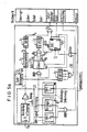
- the corresponding circuit is designated ES in FIGS. 5a and 5b.
- the clock is recovered from the supplied header bits. It is important that only the actual data appear at the output e8. Scrambled header bits and possibly dummy bits as well as end marking bits must be screened out. Delay elements such as shift registers SR1, SR3 are necessary for this. Well-defined delays are best achieved using clocked shift registers.
- the end of the header bits can be determined by a counter.
- the shift register SR2 and the bistable flip-flop F / F1 and also the counter are provided. After passing the header bits, the clock with respect to the user data is mapped in and the shift registers can work properly.
- the data packets in the transmitter contain, in addition to the header bits and the user data, so-called dummy bits, the number of which is greater than the number of the depth of the shift register used in the scrambler and in the descrambler used for decoding. Otherwise, the bit pattern of the dummy bits is arbitrary. The only thing that must not be lost is the beat that has already been won.
- the clock e2 is constantly on the descrambler.
- the dummy bits ensure that the descrambler is working properly, i.e. is synchronized when the scrambled user data enter the descrambler.
- the descrambler therefore does not have to be reset to a defined initial state before the user data begins; with e3 the user data appear correct.
- the shift registers S.R.1, S.R.2 and S.R.3 have a depth of 12 bits. Furthermore, it is assumed in the example that seven negative edge changes are contained in the scrambled header bits.
- the receiver section also includes a JAM signal detection circuit JE which gives a pulse to the computer when a JAM signal is detected.
- the retriggerable monostable multivibrator R.M.1 queries the bus for the overhead line status.
- the circuit according to FIG. 3 with regard to the handling of the header bits, possibly the dummy bits and the bits for marking the end of the data packet, and the circuits according to FIGS. 5a and 5b for the recovery of the useful data can also be applied analogously to the passive star bus.
- the circuits shown in FIGS. 2 to 5b can be constructed using modules from Texas Instruments, as can be seen, for example, from "The TTL Data Book", Texas Instruments, fourth European Edition 1980.
Landscapes
- Engineering & Computer Science (AREA)
- Computer Networks & Wireless Communication (AREA)
- Signal Processing (AREA)
- Physics & Mathematics (AREA)
- Spectroscopy & Molecular Physics (AREA)
- Power Engineering (AREA)
- Small-Scale Networks (AREA)
- Optical Communication System (AREA)
Applications Claiming Priority (2)
| Application Number | Priority Date | Filing Date | Title |
|---|---|---|---|
| DE3246241 | 1982-12-14 | ||
| DE19823246241 DE3246241A1 (de) | 1982-12-14 | 1982-12-14 | Optischer sternbus mit aktivem koppler |
Related Parent Applications (2)
| Application Number | Title | Priority Date | Filing Date |
|---|---|---|---|
| EP83112419A Division EP0117916A3 (fr) | 1982-12-14 | 1983-12-09 | Bus optique en étoile avec coupleur actif |
| EP83112419.3 Division | 1983-12-09 |
Publications (2)
| Publication Number | Publication Date |
|---|---|
| EP0254952A2 true EP0254952A2 (fr) | 1988-02-03 |
| EP0254952A3 EP0254952A3 (fr) | 1988-06-22 |
Family
ID=6180628
Family Applications (3)
| Application Number | Title | Priority Date | Filing Date |
|---|---|---|---|
| EP87110163A Withdrawn EP0305554A3 (fr) | 1982-12-14 | 1983-12-09 | Bus optique en étoile avec coupleur actif |
| EP87110167A Withdrawn EP0254952A3 (fr) | 1982-12-14 | 1983-12-09 | Système de bus optique avec un bus de données optique ainsi qu'une partie émettrice et réceptrice pour un tel système |
| EP83112419A Ceased EP0117916A3 (fr) | 1982-12-14 | 1983-12-09 | Bus optique en étoile avec coupleur actif |
Family Applications Before (1)
| Application Number | Title | Priority Date | Filing Date |
|---|---|---|---|
| EP87110163A Withdrawn EP0305554A3 (fr) | 1982-12-14 | 1983-12-09 | Bus optique en étoile avec coupleur actif |
Family Applications After (1)
| Application Number | Title | Priority Date | Filing Date |
|---|---|---|---|
| EP83112419A Ceased EP0117916A3 (fr) | 1982-12-14 | 1983-12-09 | Bus optique en étoile avec coupleur actif |
Country Status (3)
| Country | Link |
|---|---|
| EP (3) | EP0305554A3 (fr) |
| JP (1) | JPS59117841A (fr) |
| DE (1) | DE3246241A1 (fr) |
Families Citing this family (8)
| Publication number | Priority date | Publication date | Assignee | Title |
|---|---|---|---|---|
| EP0173508B1 (fr) * | 1984-08-31 | 1991-02-13 | Xerox Corporation | Réseau local |
| ATE63415T1 (de) * | 1985-09-25 | 1991-05-15 | Siemens Ag | Verfahren zum automatischen pegelabgleich in einem lokalen netz, insbesondere fuer eine mehrrechneranordnung, mit einem bussystem mit lichtwellenleitern, zum zwecke einer kollisionserkennung. |
| DE4139300A1 (de) * | 1991-11-29 | 1993-06-03 | Rheydt Kabelwerk Ag | Netzwerk-topologie zur datenuebertragung |
| US5915054A (en) * | 1992-03-05 | 1999-06-22 | Fuji Xerox Co., Ltd. | Star coupler for an optical communication network |
| EP0590331B1 (fr) * | 1992-09-01 | 2000-04-26 | Fuji Xerox Co., Ltd. | Méthode de détection de collision dans un réseau à bus |
| WO1997027685A2 (fr) * | 1996-01-29 | 1997-07-31 | Lecroy Corporation | Dispositif de controle d'un reseau en mode paquets |
| EP0910908A1 (fr) * | 1996-07-10 | 1999-04-28 | Lecroy Corporation | Procede et systeme permettant de caracteriser des equipements de fin de ligne dans un reseau local |
| GB2315626A (en) * | 1996-07-20 | 1998-02-04 | Northern Telecom Ltd | Amplified optical network |
Family Cites Families (8)
| Publication number | Priority date | Publication date | Assignee | Title |
|---|---|---|---|---|
| US3705986A (en) * | 1971-01-25 | 1972-12-12 | Computer Transmission Corp | Optical data transmission system |
| US3832028A (en) * | 1972-03-30 | 1974-08-27 | Corning Glass Works | Coupler for optical waveguide light source |
| CH559990A5 (fr) * | 1973-06-12 | 1975-03-14 | Patelhold Patentverwertung | |
| DE2409455A1 (de) * | 1974-02-27 | 1975-09-04 | Siemens Ag | Auskoppelvorrichtung fuer licht aus optischen wellenleitern |
| DE2837649A1 (de) * | 1978-08-29 | 1980-03-13 | Siemens Ag | Optisches mischerelement |
| US4245884A (en) * | 1978-12-22 | 1981-01-20 | International Business Machines Corporation | Optical coupler for interconnecting two or more optical transmission lines |
| JPS5916453B2 (ja) * | 1981-12-03 | 1984-04-16 | 株式会社リコー | 光デ−タ通信システム |
| US4531238A (en) * | 1981-12-03 | 1985-07-23 | Xerox Corporation | Statistical contention control for star configured communication networks |
-
1982
- 1982-12-14 DE DE19823246241 patent/DE3246241A1/de not_active Withdrawn
-
1983
- 1983-12-09 EP EP87110163A patent/EP0305554A3/fr not_active Withdrawn
- 1983-12-09 EP EP87110167A patent/EP0254952A3/fr not_active Withdrawn
- 1983-12-09 EP EP83112419A patent/EP0117916A3/fr not_active Ceased
- 1983-12-12 JP JP58234910A patent/JPS59117841A/ja active Pending
Non-Patent Citations (3)
| Title |
|---|
| DEUXIEME COLLOQUE INTERNATIONAL SUR LES TELECOMMUNICATIONS NUMERIQUES PAR SATELLITE, Paris, 28.-30. November 1972, Seiten 297-305, Editions Chiron, Paris, FR; A. TOMOZAWA: "D8 - Study of spectral energy dispersion for use with TDMA" * |
| LASER FOCUS, Band 18, Nr. 4, April 1982, Seiten 188,190, Newton, Massachusetts, US; "Prototype fibernet II detects data collisions" * |
| NACHRICHTENTECHN. ZEITSCHRIFT, Band 27, Heft 12, 1974, Seiten475-479, Berlin, DE; H. M]LLER: "Bit sequence independence through scramblers in digital communication systems" * |
Also Published As
| Publication number | Publication date |
|---|---|
| EP0305554A3 (fr) | 1989-04-26 |
| EP0305554A2 (fr) | 1989-03-08 |
| EP0254952A3 (fr) | 1988-06-22 |
| DE3246241A1 (de) | 1984-06-14 |
| EP0117916A2 (fr) | 1984-09-12 |
| EP0117916A3 (fr) | 1985-05-02 |
| JPS59117841A (ja) | 1984-07-07 |
Similar Documents
| Publication | Publication Date | Title |
|---|---|---|
| DE3789626T2 (de) | Wellenleiterübertragungssystem. | |
| DE3821772B4 (de) | Optische Zweiwege-Signalübertragungsvorrichtung mit einer Einrichtung zur Fehlerlokalisierung | |
| DE2733766C2 (de) | Vorrichtung zum Abtasten von auf einem Aufzeichnungsträger befindlichen codierten Daten | |
| DE3235849A1 (de) | Verfahren zum aufloesen einer kollision in einem oertlichen netzwerk | |
| DE19845248B4 (de) | Hub für einen universellen seriellen Bus und Verfahren zum Durchführen einer universellen seriellen Busübertragung in demselben | |
| DE19839238B4 (de) | Paralleles optisches Sende-/Empfangsmodul | |
| DE69733901T2 (de) | Verfahren und vorrichtung für die datenübertragung über einen lichtwellenleiter | |
| EP0254952A2 (fr) | Système de bus optique avec un bus de données optique ainsi qu'une partie émettrice et réceptrice pour un tel système | |
| DE3225773C2 (fr) | ||
| DE3224664A1 (de) | Schaltung zur erkennung von datenkollisionen in einem optischen datenbus und schaltung zur erkennung des datenfreien zustandes des busses | |
| EP0029607B1 (fr) | Système multiplex à division de temps | |
| EP0595087A1 (fr) | Récepteur pour un système de transmission d'un signal numérique sur un guide d'ondes optique dispersif | |
| DE3224425A1 (de) | Bussystem mit lichtwellenleitern | |
| DE69413366T2 (de) | Verfahren und Vorrichtung zur Feinsynchronisation von ATM-Zellen in einem optischen ATM-Knoten | |
| DE3336260A1 (de) | Verfahren und vorrichtung zur datenuebertragung | |
| DE3208008A1 (de) | Faseroptisches datenuebertragungssystem | |
| EP0834749A1 (fr) | Système et dispositif de télémétrie entre deux stations reliées par un canal de communication | |
| DE4223639C1 (de) | Verfahren zum Übertragen zweier voneinander unabhängiger digitaler Signale | |
| EP0972363B1 (fr) | Procede de transmission de signaux de donnees supplementaires et d'un signal de donnees utilisateur par l'intermediaire de liaisons optiques | |
| EP0094660B1 (fr) | Réseau local pour vitesses de transmission élevées | |
| DE3929793C2 (fr) | ||
| EP0633532B1 (fr) | Dispositif pour le contrÔle décentralisé d'accès au bus pour des unités connectées à un bus | |
| DE3235266A1 (de) | Kopplernetzwerk zum verkoppeln mehrerer teilnehmersender mit mehreren teilnehmerempfaengern | |
| EP0216167A2 (fr) | Réseau d'extension pour augmenter le nombre de raccordements d'abonnés à un système de bus passif optique avec des mélangeurs optiques | |
| DE4033540A1 (de) | Verfahren zur optischen nachrichtenuebertragung sowie optisches nachrichtenuebertragungssystem zur durchfuehrung des verfahrens |
Legal Events
| Date | Code | Title | Description |
|---|---|---|---|
| PUAI | Public reference made under article 153(3) epc to a published international application that has entered the european phase |
Free format text: ORIGINAL CODE: 0009012 |
|
| AC | Divisional application: reference to earlier application |
Ref document number: 117916 Country of ref document: EP |
|
| AK | Designated contracting states |
Kind code of ref document: A2 Designated state(s): DE FR GB IT |
|
| PUAL | Search report despatched |
Free format text: ORIGINAL CODE: 0009013 |
|
| AK | Designated contracting states |
Kind code of ref document: A3 Designated state(s): DE FR GB IT |
|
| 17P | Request for examination filed |
Effective date: 19881220 |
|
| STAA | Information on the status of an ep patent application or granted ep patent |
Free format text: STATUS: THE APPLICATION IS DEEMED TO BE WITHDRAWN |
|
| 18D | Application deemed to be withdrawn |
Effective date: 19900703 |
|
| RIN1 | Information on inventor provided before grant (corrected) |
Inventor name: WITTE, HANS-HERMANN, DR. Inventor name: MOUSTAKAS, STEVEN, DR. |