EP0255158A2 - Dispositif d'affichage des données - Google Patents
Dispositif d'affichage des données Download PDFInfo
- Publication number
- EP0255158A2 EP0255158A2 EP87201204A EP87201204A EP0255158A2 EP 0255158 A2 EP0255158 A2 EP 0255158A2 EP 87201204 A EP87201204 A EP 87201204A EP 87201204 A EP87201204 A EP 87201204A EP 0255158 A2 EP0255158 A2 EP 0255158A2
- Authority
- EP
- European Patent Office
- Prior art keywords
- display element
- display
- rectangle
- sub
- hand
- Prior art date
- Legal status (The legal status is an assumption and is not a legal conclusion. Google has not performed a legal analysis and makes no representation as to the accuracy of the status listed.)
- Withdrawn
Links
Images


Classifications
-
- G—PHYSICS
- G09—EDUCATION; CRYPTOGRAPHY; DISPLAY; ADVERTISING; SEALS
- G09F—DISPLAYING; ADVERTISING; SIGNS; LABELS OR NAME-PLATES; SEALS
- G09F9/00—Indicating arrangements for variable information in which the information is built-up on a support by selection or combination of individual elements
- G09F9/30—Indicating arrangements for variable information in which the information is built-up on a support by selection or combination of individual elements in which the desired character or characters are formed by combining individual elements
- G09F9/35—Indicating arrangements for variable information in which the information is built-up on a support by selection or combination of individual elements in which the desired character or characters are formed by combining individual elements being liquid crystals
-
- G—PHYSICS
- G09—EDUCATION; CRYPTOGRAPHY; DISPLAY; ADVERTISING; SEALS
- G09F—DISPLAYING; ADVERTISING; SIGNS; LABELS OR NAME-PLATES; SEALS
- G09F9/00—Indicating arrangements for variable information in which the information is built-up on a support by selection or combination of individual elements
- G09F9/30—Indicating arrangements for variable information in which the information is built-up on a support by selection or combination of individual elements in which the desired character or characters are formed by combining individual elements
- G09F9/302—Indicating arrangements for variable information in which the information is built-up on a support by selection or combination of individual elements in which the desired character or characters are formed by combining individual elements characterised by the form or geometrical disposition of the individual elements
Definitions
- the invention relates to a display device having at least a flat display screen, comprising an array of a plurality of substantially rectangular or parallelogram-shaped display elements in three columns.
- substantially rectangular may of course also be understood to mean square, while for example slight deviations such as roundings-off are possible.
- Combinations of display devices of this type notably for alpha-numerical data are used, for example, in information panels at airports, railway stations, banks, stadiums, etc.
- a display device of the type mentioned in the opening paragraph is described in United States Patent No. 3,936,816.
- the array shown in this Patent may relate to the positioning of (groups) of lamps or light-emitting diodes (LEDs).
- This array may be used particularly for sub-elements of gas discharge display devices or devices based on electro-luminescence. Use of these devices in conjunction with liquid crystalline material is also possible.
- the characters to be displayed are formed by selectively driving parts of a matrix of 12 squares each being partitioned diagonally in four sub-segments. In this manner 48 sub-cells are obtained which can be driven individually.
- an alpha-numerical character is often displayed by means of a 5 x 7-format dot matrix.
- oblique lines as well as those parts of the characters which by their origin have a round shape are generally displayed less satisfactorily.
- the latter characters usually give a somewhat angular impression, particularly in the slightly larger dimensions of the characters to be displayed (2 - 50 cm) which are conventional in the above-mentioned uses.
- Refinement and rounding-off by the use of, for example, a 7 x 9-format dot matrix leads to a considerable increase of the number of sub-segments and connections.
- a display device is characterized in that the display elements are arranged in accordance with at least three rows, whilst each display element comprises at most 7 sub-segments.
- the said rows themselves may consist of a plurality of sub-rows.
- a sub-row need not always cross all three columns because the arrangement of display elements in one of the columns may not permit of such a refinement.
- an embodiment of a device according to the invention is characterized in that two columns each comprises 6 display elements and the third column comprises 4 display elements, the display elements in said two columns comprising at most 4 sub-segments and those in the third column comprising at most 5 sub-segments.
- the combined display elements comprise a total of 41 sub-segments, which yields an economy of more than 15 % with respect to the device according to USP 3,936,816 and of almost 40 % with respect to display elements based on 7 x 9 format dot matrixes.
- the number of electric connections for the sub-segments may be reduced to40, if this array is used to provide, for example, electrodes of a liquid crystal display device.
- 41 electric connections are required in the case of direct drive in which only 1 counter electrode is contacted.
- a very large viewing angle may be realized over a large temperature range with this drive mode, which is extremely suitable for so-called guest-host LCD's.
- a plurality of counter electrodes may be used and may be driven by means of multiplexing, which decreases the number of required electric connections.
- 22 connections may, for example, suffice (20 for the sub-segments + 2 for the counter electrodes), in the case of 1 : 3 multiplexing even 17 connections are sufficient.
- standard IC's can be advantageously used in this case.
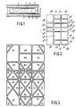
- the liquid crystalline display device shown in Figure 1 has two glass supporting plates 1 and 2 which are provided with electrodes 3 and 4 consisting of material conventionally used in LCD's. Orientation layers 7 and 8 are provided on the surfaces of the supporting plates 1 and 2 provided with electrodes. A liquid crystal material 9 is present between the supporting plates.
- each supporting plate is provided with a linear polariser, more specifically a polariser 11 and an analyser 12.
- the electrode 3 may consist of a single electrode functioning as a counter electrode for all electrodes 4 which are provided in an array to be described hereinafter. In that case direct drive is used which produces a wide viewing angle and only a slight temperature-dependence of the display properties. This mode is particularly suitable for liquid crystals of the so-called guest-host type.
- Driving may also be effected by means of multiplexing; in this case the electrode 3 is split up into, for example, 2 counter electrodes (1 : 2 multiplexing), 3 electrodes (1 : 3 multiplexing) or even more.
- the electrodes 4 are arranged in accordance with rectangular display elements 13 (Figure 2) which display elements are in turn arranged in columns 5a, 5b, 5c. As is shown in Figure 2 the display elements 13 in the columns 5 b , 5 c are arrangedin turn in accordance with sub-rows 6 a -6 f .
- the array shown may, however, also be described as an array in accordance with 3 columns 5 a , 5 b , 5 c and 3 rows in which the sub-rows 6 a , 6 b and the display element 13 a constitute a row of 3 display elements, namely 13 a and the display elements constituted by the combination of the display elements 13 e and 13 f , and13 k and 13 l , respectively.
- the row formed by combination of the sub-rows 6 c and 6 d comprises three display elements, namely the combinations 13 b , 13 c and 13 g , 13 h and 13 m and 13 n , respectively.
- the sub-rows 6 e , 6 f with display element 13 d constitute the third row in which the other display elements are formed again by combinations of the display elements 13 i and 13 j , and 13 o and 13 p , respectively.
- FIG. 3 shows how the display elements 13 a -13 p are divided into 41 sub-segments A1-A12, B1-B15 and C1-C14.
- the width of a column 5 is referred to as b and the minimum height of a display element 13 (for example 13 b ) is referred to as h, then it holds that : the display element 13 a of width b and height 3 h has a sub-segment A1 at the bottom left in the form of a right-angled triangle having sides h and 1 ⁇ 2b as legs, three sub-segments A3, A4, A5 formed by three isosceles triangles with the apex angle in the centre between the upright sides of element 13 a at a height 2h and as bases parts of the size 2h of the upright sides (A3, A4) and the lower side b (A5), respectively, and a sub-segment A2 formed by the remaining part of the display element 13 a ; the display element 13 b of
- Figure 4 shows how a number alpha-numerical characters can be displayed with these 41 sub-segments.
- the sub-segments B1 and B2 are each time driven identically so that a single connection can suffice for these segments because they may be interconnected in an electrically conducting manner.
- 41 connections are then required (40 for the segments, 1 for the counter-electrode).
- liquid crystal material such as nematic, cholesteric, chiral-nematic and ferro-electric materials or liquid crystal devices based on double refraction.
- a device may be alternatively chosen which is operated in the reflection mode. To this end the device is provided with a mirror or a mirror surface at the area of the polariser 11.
- Variations in the split-up of the elements into sub-segments and in the mutual dimensions are also possible.
- a height slightly different from h may be chosen from an esthetical point of view.
- the display element 13 d may be split up in such a manner that it contains elements similar to the elements 13 o , 13 p .
- the elements 13 d may simultaneously have a substantially identical division as 13 h , while still a drive with 41 connections remains possible, for example, by driving the sub-segments A7, A9 and C9, C11 simultaneously or by combining them to one sub-segment.
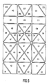
- the display device may be described as an array in three columns 5a, 5b, 5c in which the display elements 13 are arranged in accordance with 5 rows 6a-6e and in which a display element in the central column comprises at most 6 sub-segments and a display element in the outer columns comprises at most 4 sub-segments.
- Figure 6 shows how the display elements 13 a -13 o are divided in this case into 43 sub-segments A1-A13, B1-B17 and C1-C14.
- the width of a column 5 is referred to as b and the minimum height of a display element 13 (for example 13 d ) is referred to as h, then it holds that : the display element 13 a of width b and height 1.5h has a sub-segment A1 at the bottom left in the form of a right-angled triangle having sides 1,5h and 1 ⁇ 2b as legs, and a sub-segment A2 formed by the remaining part of the display element 13 a ; the display element 13 b of width b and height 3h comprises four triangular sub-segments A3, A4, A5, A6 obtained by dividing the rectangular display element in accordance with its diagonals; the display element 13 c of width b and height 3h comprises a sub-segment A7 in the form of an isosceles triangle
- the elements may also be manufactured at an angle in the form of parallelograms by having the upright sides form an angle different form 90° with the horizontal sides, starting from the sub-segments described.
- the corners may also be slightly rounded off from an esthetical point of view.
- planar array shown is, for example, also usable in gas discharge display devices or devices based on (electro-) luminescence, electrophoresis or devices based on electrochromic effects, thermo-optical or magneto-optical effects.
Landscapes
- Physics & Mathematics (AREA)
- General Physics & Mathematics (AREA)
- Engineering & Computer Science (AREA)
- Theoretical Computer Science (AREA)
- Chemical & Material Sciences (AREA)
- Crystallography & Structural Chemistry (AREA)
- Devices For Indicating Variable Information By Combining Individual Elements (AREA)
- Control Of Indicators Other Than Cathode Ray Tubes (AREA)
Applications Claiming Priority (2)
| Application Number | Priority Date | Filing Date | Title |
|---|---|---|---|
| NL8601759 | 1986-07-07 | ||
| NL8601759 | 1986-07-07 |
Publications (2)
| Publication Number | Publication Date |
|---|---|
| EP0255158A2 true EP0255158A2 (fr) | 1988-02-03 |
| EP0255158A3 EP0255158A3 (fr) | 1989-09-27 |
Family
ID=19848272
Family Applications (1)
| Application Number | Title | Priority Date | Filing Date |
|---|---|---|---|
| EP87201204A Withdrawn EP0255158A3 (fr) | 1986-07-07 | 1987-06-24 | Dispositif d'affichage des données |
Country Status (6)
| Country | Link |
|---|---|
| US (1) | US4949081A (fr) |
| EP (1) | EP0255158A3 (fr) |
| JP (1) | JPS6325688A (fr) |
| KR (1) | KR950014432B1 (fr) |
| CN (1) | CN1012111B (fr) |
| AU (1) | AU7526887A (fr) |
Cited By (7)
| Publication number | Priority date | Publication date | Assignee | Title |
|---|---|---|---|---|
| EP0338287A3 (en) * | 1988-04-15 | 1990-08-01 | Nokia-Mobira Oy | Matrix display |
| EP0421517A1 (fr) * | 1989-09-28 | 1991-04-10 | Koninklijke Philips Electronics N.V. | Dispositif de reproduction alpha-numérique |
| FR2656144A1 (fr) * | 1989-12-18 | 1991-06-21 | Asulab Sa | Dispositif electronique d'affichage. |
| WO1991008563A3 (fr) * | 1989-11-27 | 1991-09-19 | Asulab Sa | Dispositif electronique d'affichage |
| FR2711442A1 (fr) * | 1993-10-19 | 1995-04-28 | Option Ind | Afficheur de grandes dimensions formé par la juxtaposition d'une multiplicité d'éléments d'affichage. |
| GB2348038A (en) * | 1999-03-16 | 2000-09-20 | Innomind International Limited | Liquid crystal display with three-dimensional effect |
| GB2363537A (en) * | 2000-06-13 | 2001-12-19 | Motorola Inc | Pixel array for a display device |
Families Citing this family (23)
| Publication number | Priority date | Publication date | Assignee | Title |
|---|---|---|---|---|
| US5266934A (en) * | 1989-09-28 | 1993-11-30 | U.S. Philips Corporation | Alpha-numerical display device |
| US5497171A (en) * | 1989-11-27 | 1996-03-05 | Asulab S.A. | Electronic display arrangement |
| JPH05265379A (ja) * | 1992-03-18 | 1993-10-15 | Seiko Instr Inc | 液晶パネル及び表示装置及び表示方法 |
| US7167155B1 (en) | 1995-07-20 | 2007-01-23 | E Ink Corporation | Color electrophoretic displays |
| US6704133B2 (en) | 1998-03-18 | 2004-03-09 | E-Ink Corporation | Electro-optic display overlays and systems for addressing such displays |
| US7075502B1 (en) | 1998-04-10 | 2006-07-11 | E Ink Corporation | Full color reflective display with multichromatic sub-pixels |
| US6473072B1 (en) | 1998-05-12 | 2002-10-29 | E Ink Corporation | Microencapsulated electrophoretic electrostatically-addressed media for drawing device applications |
| WO2000020923A1 (fr) | 1998-10-07 | 2000-04-13 | E Ink Corporation | Systeme d'eclairage pour afficheurs electroniques non emissifs |
| US7119759B2 (en) | 1999-05-03 | 2006-10-10 | E Ink Corporation | Machine-readable displays |
| US8009348B2 (en) | 1999-05-03 | 2011-08-30 | E Ink Corporation | Machine-readable displays |
| US6486861B1 (en) * | 1999-05-07 | 2002-11-26 | Xerox Corporation | Method and apparatus for a display producing a fixed set of images |
| JP3933636B2 (ja) * | 2004-03-16 | 2007-06-20 | エーシック株式会社 | 表示装置 |
| CN102568363A (zh) * | 2012-03-20 | 2012-07-11 | 东莞市玄天电子有限公司 | 数字显示装置及其用途 |
| USD666998S1 (en) * | 2012-04-16 | 2012-09-11 | Fih (Hong Kong) Limited | Cover of an electronic device having surface ornamentation |
| USD667822S1 (en) * | 2012-04-16 | 2012-09-25 | Fih (Hong Kong) Limited | Cover of an electronic device having surface ornamentation |
| USD759064S1 (en) * | 2013-03-07 | 2016-06-14 | Samsung Electronics Co., Ltd. | Display screen with graphical user interface |
| EP2887161B1 (fr) * | 2013-12-23 | 2021-08-04 | ETA SA Manufacture Horlogère Suisse | Affichage digital comprenant un agencement d'électrodes |
| USD752020S1 (en) * | 2014-09-03 | 2016-03-22 | Zound Industries International Ab | Earphone |
| USD754639S1 (en) * | 2014-09-03 | 2016-04-26 | Plantronics, Inc. | Communications headset |
| USD784961S1 (en) * | 2015-06-05 | 2017-04-25 | Logitech Europe, S.A. | Ear cushion |
| JP1650060S (fr) * | 2019-01-09 | 2020-01-20 | ||
| USD916685S1 (en) * | 2020-06-13 | 2021-04-20 | Yanzhao Fang | Earphone |
| USD1105042S1 (en) * | 2024-05-31 | 2025-12-09 | Dongguan Hengchang Mould Plastic Co., Ltd | Pair of earphones |
Family Cites Families (13)
| Publication number | Priority date | Publication date | Assignee | Title |
|---|---|---|---|---|
| US3802723A (en) * | 1972-04-05 | 1974-04-09 | A Watson | Method for binding a book |
| FR2184188A5 (fr) * | 1972-05-10 | 1973-12-21 | Thomson Csf T Vt Sa | |
| US3936816A (en) * | 1972-11-02 | 1976-02-03 | Dai Nippon Toryo Kabushiki Kaisha | Flat display system |
| CH566610A5 (fr) * | 1973-01-03 | 1975-09-15 | Battelle Memorial Institute | |
| JPS52107723A (en) * | 1974-12-28 | 1977-09-09 | Seikosha Kk | Device for forming picture |
| FR2309941A1 (fr) * | 1975-05-02 | 1976-11-26 | Cii | Dispositif d'affichage de plusieurs signes sur une meme aire de visualisation |
| JPS53125797A (en) * | 1977-04-08 | 1978-11-02 | Masaru Nanjiyou | Character pattern for display |
| US4237459A (en) * | 1978-12-21 | 1980-12-02 | Eric F. Burtis | Visual display with illuminable elements arranged in vertically aligned sections |
| US4342031A (en) * | 1980-01-15 | 1982-07-27 | The Laitram Corporation | Liquid crystal and numerical display devices |
| JPS576882A (en) * | 1980-06-16 | 1982-01-13 | Hitachi Ltd | Liquid crystal display element |
| GB2151832B (en) * | 1983-12-16 | 1987-08-19 | Standard Telephones Cables Ltd | Electro optic flat panel display |
| JPS6150184A (ja) * | 1984-08-17 | 1986-03-12 | 津田工業株式会社 | シフトポジシヨン表示装置 |
| CH661373A5 (de) * | 1984-09-11 | 1987-07-15 | Autophon Ag | Alphanumerische anzeigeanlage mit in je einen sichtbaren und einen unsichtbaren zustand steuerbaren segmenten. |
-
1987
- 1987-06-24 EP EP87201204A patent/EP0255158A3/fr not_active Withdrawn
- 1987-07-04 KR KR1019870007134A patent/KR950014432B1/ko not_active Expired - Fee Related
- 1987-07-04 CN CN87104666A patent/CN1012111B/zh not_active Expired
- 1987-07-06 AU AU75268/87A patent/AU7526887A/en not_active Abandoned
- 1987-07-07 JP JP62167944A patent/JPS6325688A/ja active Pending
-
1988
- 1988-12-09 US US07/282,148 patent/US4949081A/en not_active Expired - Fee Related
Cited By (8)
| Publication number | Priority date | Publication date | Assignee | Title |
|---|---|---|---|---|
| EP0338287A3 (en) * | 1988-04-15 | 1990-08-01 | Nokia-Mobira Oy | Matrix display |
| EP0421517A1 (fr) * | 1989-09-28 | 1991-04-10 | Koninklijke Philips Electronics N.V. | Dispositif de reproduction alpha-numérique |
| WO1991008563A3 (fr) * | 1989-11-27 | 1991-09-19 | Asulab Sa | Dispositif electronique d'affichage |
| FR2656144A1 (fr) * | 1989-12-18 | 1991-06-21 | Asulab Sa | Dispositif electronique d'affichage. |
| FR2711442A1 (fr) * | 1993-10-19 | 1995-04-28 | Option Ind | Afficheur de grandes dimensions formé par la juxtaposition d'une multiplicité d'éléments d'affichage. |
| GB2348038A (en) * | 1999-03-16 | 2000-09-20 | Innomind International Limited | Liquid crystal display with three-dimensional effect |
| GB2348038B (en) * | 1999-03-16 | 2002-03-27 | Innomind Internat Ltd | Display, and device having a display |
| GB2363537A (en) * | 2000-06-13 | 2001-12-19 | Motorola Inc | Pixel array for a display device |
Also Published As
| Publication number | Publication date |
|---|---|
| KR950014432B1 (ko) | 1995-11-27 |
| JPS6325688A (ja) | 1988-02-03 |
| CN1012111B (zh) | 1991-03-20 |
| EP0255158A3 (fr) | 1989-09-27 |
| AU7526887A (en) | 1988-01-14 |
| US4949081A (en) | 1990-08-14 |
| KR880002117A (ko) | 1988-04-29 |
| CN87104666A (zh) | 1988-01-13 |
Similar Documents
| Publication | Publication Date | Title |
|---|---|---|
| US4949081A (en) | Data display device | |
| EP1370904B1 (fr) | Dispositif d'affichage par electrophorese | |
| US4373784A (en) | Electrode structure on a matrix type liquid crystal panel | |
| US4764766A (en) | Method for driving and liquid crystal display device including dot matrix display part and fixed pattern display port | |
| US4099855A (en) | Liquid crystal display arrangements | |
| WO1995014949A3 (fr) | Dispositif de visualisation par transparence comprenant un ecran a cristaux liquides a matrice passive | |
| GB2268306A (en) | Large area liquid crystal displays | |
| US6486861B1 (en) | Method and apparatus for a display producing a fixed set of images | |
| JPS60151690A (ja) | 英数字表示用電気光学フラツトパネルデイスプレイ装置 | |
| EP1343137A3 (fr) | Circuit de commande unipolaire pour des afficheurs à cristaux liquides cholestériques | |
| JPS6031120A (ja) | 液晶装置 | |
| CN102231025A (zh) | 多畴垂直配向型液晶显示面板及其像素结构 | |
| US8587570B2 (en) | LCD display element with reduce crosstalk at the intersection of row leads and row electrodes | |
| US5266934A (en) | Alpha-numerical display device | |
| US4932756A (en) | Display character | |
| CA2296174A1 (fr) | Affichage a cristaux liquides offrant une meilleure lisibilite de caracteres | |
| GB2067814A (en) | Liquid crystal matrix display device | |
| JPS5836346B2 (ja) | マトリクス素子による光学装置 | |
| KR940006349B1 (ko) | 표시 장치 | |
| CN219016759U (zh) | 基板结构和具有其的电子纸显示屏和电子设备 | |
| JPH03138686A (ja) | 文字数字表示装置 | |
| CA2058902A1 (fr) | Afficheur a cristaux liquides | |
| KR880004417A (ko) | 디스플레이 장치 | |
| JPS60222897A (ja) | フラツトパネル表示装置 | |
| CN85103239A (zh) | 液晶显示器件 |
Legal Events
| Date | Code | Title | Description |
|---|---|---|---|
| PUAI | Public reference made under article 153(3) epc to a published international application that has entered the european phase |
Free format text: ORIGINAL CODE: 0009012 |
|
| AK | Designated contracting states |
Kind code of ref document: A2 Designated state(s): CH DE ES FR GB IT LI NL SE |
|
| PUAL | Search report despatched |
Free format text: ORIGINAL CODE: 0009013 |
|
| AK | Designated contracting states |
Kind code of ref document: A3 Designated state(s): CH DE ES FR GB IT LI NL SE |
|
| 17P | Request for examination filed |
Effective date: 19900322 |
|
| 17Q | First examination report despatched |
Effective date: 19930603 |
|
| GRAG | Despatch of communication of intention to grant |
Free format text: ORIGINAL CODE: EPIDOS AGRA |
|
| STAA | Information on the status of an ep patent application or granted ep patent |
Free format text: STATUS: THE APPLICATION IS DEEMED TO BE WITHDRAWN |
|
| 18D | Application deemed to be withdrawn |
Effective date: 19971219 |
|
| RIN1 | Information on inventor provided before grant (corrected) |
Inventor name: KELLER, DANIEL ROBERT Inventor name: SCHELLING, ANDREAS DANIEL |