EP0255309A2 - Elektronische Registrierkasse - Google Patents
Elektronische Registrierkasse Download PDFInfo
- Publication number
- EP0255309A2 EP0255309A2 EP19870306589 EP87306589A EP0255309A2 EP 0255309 A2 EP0255309 A2 EP 0255309A2 EP 19870306589 EP19870306589 EP 19870306589 EP 87306589 A EP87306589 A EP 87306589A EP 0255309 A2 EP0255309 A2 EP 0255309A2
- Authority
- EP
- European Patent Office
- Prior art keywords
- memory
- data
- file
- regions
- cash register
- Prior art date
- Legal status (The legal status is an assumption and is not a legal conclusion. Google has not performed a legal analysis and makes no representation as to the accuracy of the status listed.)
- Granted
Links
Images




Classifications
-
- G—PHYSICS
- G07—CHECKING-DEVICES
- G07G—REGISTERING THE RECEIPT OF CASH, VALUABLES, OR TOKENS
- G07G1/00—Cash registers
- G07G1/12—Cash registers electronically operated
-
- G—PHYSICS
- G06—COMPUTING OR CALCULATING; COUNTING
- G06Q—INFORMATION AND COMMUNICATION TECHNOLOGY [ICT] SPECIALLY ADAPTED FOR ADMINISTRATIVE, COMMERCIAL, FINANCIAL, MANAGERIAL OR SUPERVISORY PURPOSES; SYSTEMS OR METHODS SPECIALLY ADAPTED FOR ADMINISTRATIVE, COMMERCIAL, FINANCIAL, MANAGERIAL OR SUPERVISORY PURPOSES, NOT OTHERWISE PROVIDED FOR
- G06Q20/00—Payment architectures, schemes or protocols
- G06Q20/08—Payment architectures
- G06Q20/20—Point-of-sale [POS] network systems
Definitions
- the present invention relates to an electronic cash register useful for cash transfer accompanying the sale of commodities, say, at a store.
- An object of the present invention is to provide an electronic cash register capable of setting desirably the memory capacity of each storage region allocated in the RAM for storing each of different accumulated data as well as of erasing a particular storage region or generating a required storage region in the RAM.
- an electronic cash register comprises key input means having a plurality of operation keys, memory means comprising a plurality of storage regions for storing a plurality of accumulated data of different kinds, and means for controlling the key input means and the memory means.
- the control means controls the memory means so as to increase or decrease the memory capacity of any particular storage region, erase any desired storage region, or generate a required storage region in the memory means.
- Fig. 1 is an electric circuit block diagram of an embodiment of an electronic cash register (hereinafter abbreviated as ECR) 11 of the present invention.
- the ECR 11 comprises a central processing unit (CPU) 12 as control means, a random-access-memory (RAM) 13 as memory means, a read-only-memory (ROM) 14, display means 15, printing means 16, key input means 17 having a plurality of operation keys, and a drawer 18 for storing cash.
- Fig. 2 is a plan view of the key input means 17. As shown, a plurality of operation keys are arranged on the key input means 17.
- the ROM 14 stores control procedures (programs) according to which the CPU 12 executes control operation when instructed by a signal input given by key operation from the key input means 17.
- the control result is stored in the RAM 13, and if required by the operator, presented on the display means 15 and printed out by the printing means 16.
- Fig. 3 shows the structure of the storage regions in the RAM 13.
- the RAM 13 comprises file descriptor regions 19 and file data regions 20.
- the file descriptor regions 19 have a fixed memory capacity and store start address, end address and data structure of the file data regions (described later) 20 for each file (Here, a file referred to each storage region allocated in the RAM 13).
- Write/read for each file is controlled through the file descriptor regions. Specifically, write/read for the No. 1 file data region DA1 is controlled through the descriptor region DS1, and that for subsequent file data regions through the corresponding descriptor regions DS2, DS3, ...
- the file data regions 20 store various accumulated data by file.
- the memory capacity of each file data region for a file is variable; when there is no file, the capacity of the file data region is zero.
- ECR 11 Operation of the ECR 11 of the above construction is described below: It is assumed that the ECR 11 with the RAM 13 having such file allocation as shown in Fig. 4(1) is used in a store. Each file is allotted with file number.
- a department memory region 21 which is one of the files is set in advance to have a memory capacity for storing up to 40 departments. The number of departments may increase or decrease as the store is expanded or reduced in scale. The memory capacity of the department memory region 21 may be increased or decreased to be accommodated to the change in the number of departments.
- a specified unit of data storage such as the memory capacity for one department is called a record.
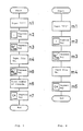
- Fig. 5 shows the flow chart of the operation for setting the number of records in a particular file.
- the operator inputs "971" for designating the program for this operation (Step n1), depresses ".” key 23 on the key input means 17 (Step n2) and "@/FOR” key 24 (Step n3), inputs the file No. of the department memory region (Step n4), depresses "@/FOR” key 24 again (Step n5), and inputs the desired number of records (Step n6). Finally, the operator depresses "CA” key 25 to end the procedure. A desired memory capacity is thus set for the file.
- Figs. 4(2) and 4(3) show the file allocation in the RAM 13 where the memory capacity of the department memory region 21 is increased from 40 departments to 100 departments and where the memory capacity of the department memory 21 is decreased to 20 departments, respectively.
- Fig. 7 shows the structure of a file in which the records are not grouped
- Fig. 8 shows the structure of a file in which the records are grouped into a plurality of blocks
- Figs. 9 and 10 show two specific examples of record data arrangement in a file.
- M records are stored in a file capable of storing up to N records.
- Each of the records R1, R2, ..., RM comprises sixteen fields.
- the first field F1 stores label data L1, L2, ..., LM.
- the memory capacity for each record is 256 bytes.
- M and N have the relationship expressed as: 0 ⁇ M ⁇ N ⁇ 65535 Vietnamese (1).
- the records are stored successively in a file with no open space between adjacent records.
- the area indicated by E in Fig. 7 is empty with no data stored.
- Fig. 9 shows the data arrangement in the record R1, one of the records in Fig. 7.
- the data "1A" in the first field F1 represents the department name "department of fruit".
- the data "0000098400" in the second field F2 represents the sale proceeds of ⁇ 9840.
- "00001230" in the third field F3 indicates that the number of commodities sold is 123.
- the data "4F52414E47452020" in the sixth field F6 is the ASCII code indicating that the data is related to "oranges”.
- Fig. 8 shows the structure of a file for accumulated sales data for each salesman.
- the memory capacity of the 4th to the 16th fields of each record is set to zero.
- This file is divided into a plurality of blocks, each containing data for a different salesman.
- Each block is capable of storing up to H records.
- I records are stored in each block.
- the file structure of the first block B1 is identical with that shown in Fig. 7.
- the second block B2 and the subsequent blocks do not contain the first field; the first field in the first block B1 is shared by all the other blocks.
- the first record Rb21 in the second block B2 uses the label data "Label 1" of the first record Rb11 in the first block B1.
- Fig. 10 shows the data arrangement in the record Rb11 shown in Fig. 8.
- "434131" in the first field Fb1 is the ASCII code representing a record data name.
- "0001234000” in the second field Fb2 represents the sale proceeds of ⁇ 123400.
- the data "007890" in the third field Fb3 indicates that the number of transactions is 789.
- the type of the data thus stored in each record of a file is limited to two kinds: so-called packed decimal data and binary data.
- the packed decimal data is a numeric data having a number of two figures in a byte plus a sign.
- the sign is set in the lower four bits in the last byte; the lower four bits are set to "0000" for a positive number, "1101” for a negative number, "1010” for a positive overflow data, and "1011” for a negative overflow data.
- the data in the second field F2 and in the third field F3 shown in Fig. 9 are packed decimal data.
- the binary data is a byte of data expressed in the hexadecimal notation "00"(H) to "FF"(H) or by binary numbers "00000000” to "11111111” in the binary notation.
- the data in the first field F1 and in the sixth field F6 of Fig 9 are binary data.
- the ECR 11 is capable of changing the number of blocks in a particular field.
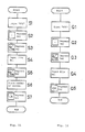
- Fig. 11 is a flow chart showing the procedure of changing the number of blocks.
- the operator inputs "972" for designating the program for this operation (Step S1), depresses ".” key 23 (Step S2) and then "@/FOR” key 24 (Step S3), inputs file No. of the file whose number of blocks is to be changed (Step S4), depresses "@/FOR” key 24 again (Step S5), inputs desired number of blocks (Step S6), and depresses "CA” key 25 to end the procedure (Step S7).
- Fig. 12 is a flow chart showing the procedure of generating a new file in the RAM 13.
- the new file is stored in advance in separate storage means (not shown). To generate a new file, therefore, it is necessary to connect the separate storage means to the ECR 11.
- the operator inputs "970" to designate the program for the new file generation (Step Q1), depresses ".” key 23 (Step Q2) and then "@/FOR” key 24 (Step Q3), inputs file No. of the file to be generated (Step Q4), and depresses "CA” key 24 to end the procedure (Step Q5).
- a desired file can be thus generated in the RAM 13.
- the operation of generating/erasing a file and that of changing the number of records or blocks as mentioned above are executed under control of the CPU 12. It is understood that the ECR 11 of the present invention is capable of varying the memory capacity of a particular storage region as desired, erasing any particular storage portion, and generating a new storage region in the RAM 13.
- control means controls memory means so as to change the memory capacity of any particular storage region, erase an unnecessary storage portion, or generate a new storage region in the memory means. Accordingly, it is possible to select only necessary data for storage from various accumulated data and to vary the memory capacity depending on the amount of data to be stored.
- the present invention therefore allows the memory means to be used as effectively as possible, enhancing the usefulness of the electronic cash register remarkably.
- the memory capacities of the storage regions allocated in the memory means for storing various accumulated data are varied, any particular storage regions are erased, and new storage regions are generated in the memory means, under control of the control means simply by key operation on the key input means, so that the operation for, say, increasing the memory capacity for a particular accumulated data is very easy. It should be understood, therefore, that the present invention permits the most effective use of the memory means.
Landscapes
- Business, Economics & Management (AREA)
- Physics & Mathematics (AREA)
- General Physics & Mathematics (AREA)
- Accounting & Taxation (AREA)
- Finance (AREA)
- Strategic Management (AREA)
- General Business, Economics & Management (AREA)
- Engineering & Computer Science (AREA)
- Theoretical Computer Science (AREA)
- Cash Registers Or Receiving Machines (AREA)
- Information Retrieval, Db Structures And Fs Structures Therefor (AREA)
Applications Claiming Priority (2)
| Application Number | Priority Date | Filing Date | Title |
|---|---|---|---|
| JP61181705A JPS6336490A (ja) | 1986-07-31 | 1986-07-31 | 電子式金銭登録機 |
| JP181705/86 | 1986-07-31 |
Publications (3)
| Publication Number | Publication Date |
|---|---|
| EP0255309A2 true EP0255309A2 (de) | 1988-02-03 |
| EP0255309A3 EP0255309A3 (en) | 1989-08-16 |
| EP0255309B1 EP0255309B1 (de) | 1993-09-15 |
Family
ID=16105413
Family Applications (1)
| Application Number | Title | Priority Date | Filing Date |
|---|---|---|---|
| EP87306589A Expired - Lifetime EP0255309B1 (de) | 1986-07-31 | 1987-07-24 | Elektronische Registrierkasse |
Country Status (4)
| Country | Link |
|---|---|
| US (1) | US4893236A (de) |
| EP (1) | EP0255309B1 (de) |
| JP (1) | JPS6336490A (de) |
| DE (1) | DE3787422T2 (de) |
Cited By (1)
| Publication number | Priority date | Publication date | Assignee | Title |
|---|---|---|---|---|
| GB2269925A (en) * | 1992-08-19 | 1994-02-23 | Matsushita Electric Industrial Co Ltd | Electronic cash register |
Families Citing this family (9)
| Publication number | Priority date | Publication date | Assignee | Title |
|---|---|---|---|---|
| US5189607A (en) * | 1987-10-31 | 1993-02-23 | Sharp Kabushiki Kaisha | Method for sending selected data from electronic cash registers to a host unit |
| DE3915645C2 (de) * | 1989-05-12 | 1995-11-16 | Mettler Toledo Albstadt Gmbh | Preisrechnende elektronische Waage |
| US5263164A (en) | 1991-01-09 | 1993-11-16 | Verifone, Inc. | Method and structure for determining transaction system hardware and software configurations |
| JP3445304B2 (ja) * | 1993-03-29 | 2003-09-08 | 株式会社東芝 | ファイル管理装置 |
| JP3594980B2 (ja) * | 1993-12-10 | 2004-12-02 | 株式会社東芝 | ファイル管理方式 |
| US7555458B1 (en) * | 1996-06-05 | 2009-06-30 | Fraud Control System.Com Corporation | Method of billing a purchase made over a computer network |
| US8229844B2 (en) | 1996-06-05 | 2012-07-24 | Fraud Control Systems.Com Corporation | Method of billing a purchase made over a computer network |
| US20030195846A1 (en) * | 1996-06-05 | 2003-10-16 | David Felger | Method of billing a purchase made over a computer network |
| US7472394B1 (en) | 2000-07-07 | 2008-12-30 | Paymentech, L.P. | System and method for programming point of sale devices |
Family Cites Families (11)
| Publication number | Priority date | Publication date | Assignee | Title |
|---|---|---|---|---|
| JPS51131238A (en) * | 1975-05-10 | 1976-11-15 | Tokyo Electric Co Ltd | Electronic register |
| DE2726860C3 (de) * | 1976-06-16 | 1979-12-13 | Tokyo Electric Co., Ltd., Tokio | Anordnung zum Voreinstellen von Einheitspreisen bei einer Registrierkasse |
| JPS5820071B2 (ja) * | 1979-06-15 | 1983-04-21 | オムロン株式会社 | 電子式キヤツシユレジスタの群管理方式 |
| GB2058424B (en) * | 1979-09-10 | 1983-06-08 | Casio Computer Co Ltd | Electronic cash register |
| US4328544A (en) * | 1980-01-04 | 1982-05-04 | International Business Machines Corporation | Electronic point-of-sale system using direct-access storage |
| DE3175615D1 (en) * | 1980-12-24 | 1987-01-02 | Olivetti & Co Spa | Data recording machine |
| US4475176A (en) * | 1981-08-06 | 1984-10-02 | Tokyo Shibaura Denki Kabushiki Kaisha | Memory control system |
| JPS59100977A (ja) * | 1982-12-01 | 1984-06-11 | Omron Tateisi Electronics Co | 記録情報出力方法 |
| JPS60153593A (ja) * | 1984-01-24 | 1985-08-13 | カシオ計算機株式会社 | 電子レジスタ |
| JPS60205644A (ja) * | 1984-03-29 | 1985-10-17 | Ascii Corp | メモリアドレス拡張方式 |
| US4729097A (en) * | 1984-05-11 | 1988-03-01 | Tokyo Electric Co., Ltd. | Sales registration apparatus with means to transfer control program and sales registration data between individual units |
-
1986
- 1986-07-31 JP JP61181705A patent/JPS6336490A/ja active Pending
-
1987
- 1987-07-24 EP EP87306589A patent/EP0255309B1/de not_active Expired - Lifetime
- 1987-07-24 DE DE87306589T patent/DE3787422T2/de not_active Expired - Fee Related
- 1987-07-31 US US07/080,568 patent/US4893236A/en not_active Expired - Lifetime
Cited By (3)
| Publication number | Priority date | Publication date | Assignee | Title |
|---|---|---|---|---|
| GB2269925A (en) * | 1992-08-19 | 1994-02-23 | Matsushita Electric Industrial Co Ltd | Electronic cash register |
| GB2269925B (en) * | 1992-08-19 | 1996-08-21 | Matsushita Electric Industrial Co Ltd | Electronic cash register and system including the same |
| US5805831A (en) * | 1992-08-19 | 1998-09-08 | Matsushita Electric Industrial Co., Ltd. | Electronic cash register system allocating sale items in designated chit bills or receipt files |
Also Published As
| Publication number | Publication date |
|---|---|
| US4893236A (en) | 1990-01-09 |
| EP0255309B1 (de) | 1993-09-15 |
| EP0255309A3 (en) | 1989-08-16 |
| JPS6336490A (ja) | 1988-02-17 |
| DE3787422D1 (de) | 1993-10-21 |
| DE3787422T2 (de) | 1994-04-14 |
Similar Documents
| Publication | Publication Date | Title |
|---|---|---|
| US4486857A (en) | Display system for the suppression and regeneration of characters in a series of fields in a stored record | |
| US5812841A (en) | Method and apparatus for recording and reading date data having coexisting formats | |
| CA1165449A (en) | Qualifying and sorting file record data | |
| US4903018A (en) | Process for compressing and expanding structurally associated multiple-data sequences, and arrangements for implementing the process | |
| US3611316A (en) | Indirect indexed searching and sorting | |
| US4893236A (en) | Electronic cash register | |
| Blaauw et al. | The structure of SYSTEM/360: Part I—Outline of the logical structure | |
| US3771142A (en) | Digital data storage system | |
| US6931507B2 (en) | Memory allocation method using multi-level partition | |
| GB2294564A (en) | Hash system for transforming records to be hashed | |
| US3964028A (en) | System and method for evaluating paging behavior | |
| EP0167959A2 (de) | Rechner-Vektorregisterverarbeitung | |
| US4114026A (en) | Electronic desk-top accounting machine and calculator | |
| US7093096B2 (en) | Optimised management method for allocating memory workspace of an onboard system and corresponding onboard system | |
| US4959778A (en) | Address space switching apparatus | |
| GB886421A (en) | Improvements in or relating to data processing apparatus | |
| US4751631A (en) | Apparatus for fast generation of signal sequences | |
| US6086632A (en) | Register optimizing compiler using commutative operations | |
| JPH01246664A (ja) | データ処理装置 | |
| US5930505A (en) | Method for storing a program into an auxiliary memory | |
| US4831569A (en) | Display system for indicating standby operations of electronic data processing apparatus | |
| EP0075633A1 (de) | Registerzuordnungsanordnung | |
| EP0065114B1 (de) | Verfahren zur Qualifizierung und Sortierung von Informationen von einem Aufzeichnungssatzesspeicher in einem Textverarbeitungssystem | |
| US3081447A (en) | Apparatus and methods for automatic indexing and storage | |
| JPS5987567A (ja) | 可変長デ−タ記憶制御方式 |
Legal Events
| Date | Code | Title | Description |
|---|---|---|---|
| PUAI | Public reference made under article 153(3) epc to a published international application that has entered the european phase |
Free format text: ORIGINAL CODE: 0009012 |
|
| AK | Designated contracting states |
Kind code of ref document: A2 Designated state(s): DE GB IT |
|
| PUAL | Search report despatched |
Free format text: ORIGINAL CODE: 0009013 |
|
| AK | Designated contracting states |
Kind code of ref document: A3 Designated state(s): DE GB IT |
|
| 17P | Request for examination filed |
Effective date: 19891227 |
|
| 17Q | First examination report despatched |
Effective date: 19910924 |
|
| GRAA | (expected) grant |
Free format text: ORIGINAL CODE: 0009210 |
|
| AK | Designated contracting states |
Kind code of ref document: B1 Designated state(s): DE GB IT |
|
| RIN1 | Information on inventor provided before grant (corrected) |
Inventor name: GOTO, KAZUYUKI Inventor name: KOMAI, KENSAKU Inventor name: NAKAMURA, YASUHIDE Inventor name: OHNISHI, SOUICHI |
|
| REF | Corresponds to: |
Ref document number: 3787422 Country of ref document: DE Date of ref document: 19931021 |
|
| ITF | It: translation for a ep patent filed | ||
| PLBE | No opposition filed within time limit |
Free format text: ORIGINAL CODE: 0009261 |
|
| STAA | Information on the status of an ep patent application or granted ep patent |
Free format text: STATUS: NO OPPOSITION FILED WITHIN TIME LIMIT |
|
| 26N | No opposition filed | ||
| PGFP | Annual fee paid to national office [announced via postgrant information from national office to epo] |
Ref country code: DE Payment date: 20010716 Year of fee payment: 15 |
|
| PGFP | Annual fee paid to national office [announced via postgrant information from national office to epo] |
Ref country code: GB Payment date: 20010718 Year of fee payment: 15 |
|
| REG | Reference to a national code |
Ref country code: GB Ref legal event code: IF02 |
|
| PG25 | Lapsed in a contracting state [announced via postgrant information from national office to epo] |
Ref country code: GB Free format text: LAPSE BECAUSE OF NON-PAYMENT OF DUE FEES Effective date: 20020724 |
|
| PG25 | Lapsed in a contracting state [announced via postgrant information from national office to epo] |
Ref country code: DE Free format text: LAPSE BECAUSE OF NON-PAYMENT OF DUE FEES Effective date: 20030201 |
|
| GBPC | Gb: european patent ceased through non-payment of renewal fee |
Effective date: 20020724 |
|
| PG25 | Lapsed in a contracting state [announced via postgrant information from national office to epo] |
Ref country code: IT Free format text: LAPSE BECAUSE OF NON-PAYMENT OF DUE FEES;WARNING: LAPSES OF ITALIAN PATENTS WITH EFFECTIVE DATE BEFORE 2007 MAY HAVE OCCURRED AT ANY TIME BEFORE 2007. THE CORRECT EFFECTIVE DATE MAY BE DIFFERENT FROM THE ONE RECORDED. Effective date: 20050724 |