EP0255557A2 - Procédé de formation d'images métalliques - Google Patents
Procédé de formation d'images métalliques Download PDFInfo
- Publication number
- EP0255557A2 EP0255557A2 EP86112660A EP86112660A EP0255557A2 EP 0255557 A2 EP0255557 A2 EP 0255557A2 EP 86112660 A EP86112660 A EP 86112660A EP 86112660 A EP86112660 A EP 86112660A EP 0255557 A2 EP0255557 A2 EP 0255557A2
- Authority
- EP
- European Patent Office
- Prior art keywords
- coating
- organic coating
- soluble
- organic
- copper
- Prior art date
- Legal status (The legal status is an assumption and is not a legal conclusion. Google has not performed a legal analysis and makes no representation as to the accuracy of the status listed.)
- Withdrawn
Links
Images
Classifications
-
- H—ELECTRICITY
- H05—ELECTRIC TECHNIQUES NOT OTHERWISE PROVIDED FOR
- H05K—PRINTED CIRCUITS; CASINGS OR CONSTRUCTIONAL DETAILS OF ELECTRIC APPARATUS; MANUFACTURE OF ASSEMBLAGES OF ELECTRICAL COMPONENTS
- H05K3/00—Apparatus or processes for manufacturing printed circuits
- H05K3/02—Apparatus or processes for manufacturing printed circuits in which the conductive material is applied to the surface of the insulating support and is thereafter removed from such areas of the surface which are not intended for current conducting or shielding
- H05K3/06—Apparatus or processes for manufacturing printed circuits in which the conductive material is applied to the surface of the insulating support and is thereafter removed from such areas of the surface which are not intended for current conducting or shielding the conductive material being removed chemically or electrolytically, e.g. by photo-etch process
- H05K3/061—Etching masks
-
- G—PHYSICS
- G03—PHOTOGRAPHY; CINEMATOGRAPHY; ANALOGOUS TECHNIQUES USING WAVES OTHER THAN OPTICAL WAVES; ELECTROGRAPHY; HOLOGRAPHY
- G03F—PHOTOMECHANICAL PRODUCTION OF TEXTURED OR PATTERNED SURFACES, e.g. FOR PRINTING, FOR PROCESSING OF SEMICONDUCTOR DEVICES; MATERIALS THEREFOR; ORIGINALS THEREFOR; APPARATUS SPECIALLY ADAPTED THEREFOR
- G03F7/00—Photomechanical, e.g. photolithographic, production of textured or patterned surfaces, e.g. printing surfaces; Materials therefor, e.g. comprising photoresists; Apparatus specially adapted therefor
-
- G—PHYSICS
- G03—PHOTOGRAPHY; CINEMATOGRAPHY; ANALOGOUS TECHNIQUES USING WAVES OTHER THAN OPTICAL WAVES; ELECTROGRAPHY; HOLOGRAPHY
- G03F—PHOTOMECHANICAL PRODUCTION OF TEXTURED OR PATTERNED SURFACES, e.g. FOR PRINTING, FOR PROCESSING OF SEMICONDUCTOR DEVICES; MATERIALS THEREFOR; ORIGINALS THEREFOR; APPARATUS SPECIALLY ADAPTED THEREFOR
- G03F7/00—Photomechanical, e.g. photolithographic, production of textured or patterned surfaces, e.g. printing surfaces; Materials therefor, e.g. comprising photoresists; Apparatus specially adapted therefor
- G03F7/16—Coating processes; Apparatus therefor
- G03F7/164—Coating processes; Apparatus therefor using electric, electrostatic or magnetic means; powder coating
-
- H—ELECTRICITY
- H05—ELECTRIC TECHNIQUES NOT OTHERWISE PROVIDED FOR
- H05K—PRINTED CIRCUITS; CASINGS OR CONSTRUCTIONAL DETAILS OF ELECTRIC APPARATUS; MANUFACTURE OF ASSEMBLAGES OF ELECTRICAL COMPONENTS
- H05K3/00—Apparatus or processes for manufacturing printed circuits
- H05K3/10—Apparatus or processes for manufacturing printed circuits in which conductive material is applied to the insulating support in such a manner as to form the desired conductive pattern
- H05K3/108—Apparatus or processes for manufacturing printed circuits in which conductive material is applied to the insulating support in such a manner as to form the desired conductive pattern by semi-additive methods; masks therefor
-
- H—ELECTRICITY
- H05—ELECTRIC TECHNIQUES NOT OTHERWISE PROVIDED FOR
- H05K—PRINTED CIRCUITS; CASINGS OR CONSTRUCTIONAL DETAILS OF ELECTRIC APPARATUS; MANUFACTURE OF ASSEMBLAGES OF ELECTRICAL COMPONENTS
- H05K3/00—Apparatus or processes for manufacturing printed circuits
- H05K3/22—Secondary treatment of printed circuits
- H05K3/24—Reinforcing of the conductive pattern
- H05K3/243—Reinforcing of the conductive pattern characterised by selective plating, e.g. for finish plating of pads
-
- H—ELECTRICITY
- H05—ELECTRIC TECHNIQUES NOT OTHERWISE PROVIDED FOR
- H05K—PRINTED CIRCUITS; CASINGS OR CONSTRUCTIONAL DETAILS OF ELECTRIC APPARATUS; MANUFACTURE OF ASSEMBLAGES OF ELECTRICAL COMPONENTS
- H05K1/00—Printed circuits
- H05K1/02—Details
- H05K1/11—Printed elements for providing electric connections to or between printed circuits
- H05K1/117—Pads along the edge of rigid circuit boards, e.g. for pluggable connectors
-
- H—ELECTRICITY
- H05—ELECTRIC TECHNIQUES NOT OTHERWISE PROVIDED FOR
- H05K—PRINTED CIRCUITS; CASINGS OR CONSTRUCTIONAL DETAILS OF ELECTRIC APPARATUS; MANUFACTURE OF ASSEMBLAGES OF ELECTRICAL COMPONENTS
- H05K2201/00—Indexing scheme relating to printed circuits covered by H05K1/00
- H05K2201/03—Conductive materials
- H05K2201/0332—Structure of the conductor
- H05K2201/0335—Layered conductors or foils
- H05K2201/0355—Metal foils
-
- H—ELECTRICITY
- H05—ELECTRIC TECHNIQUES NOT OTHERWISE PROVIDED FOR
- H05K—PRINTED CIRCUITS; CASINGS OR CONSTRUCTIONAL DETAILS OF ELECTRIC APPARATUS; MANUFACTURE OF ASSEMBLAGES OF ELECTRICAL COMPONENTS
- H05K2203/00—Indexing scheme relating to apparatus or processes for manufacturing printed circuits covered by H05K3/00
- H05K2203/05—Patterning and lithography; Masks; Details of resist
- H05K2203/0562—Details of resist
- H05K2203/0582—Coating by resist, i.e. resist used as mask for application of insulating coating or of second resist
-
- H—ELECTRICITY
- H05—ELECTRIC TECHNIQUES NOT OTHERWISE PROVIDED FOR
- H05K—PRINTED CIRCUITS; CASINGS OR CONSTRUCTIONAL DETAILS OF ELECTRIC APPARATUS; MANUFACTURE OF ASSEMBLAGES OF ELECTRICAL COMPONENTS
- H05K2203/00—Indexing scheme relating to apparatus or processes for manufacturing printed circuits covered by H05K3/00
- H05K2203/07—Treatments involving liquids, e.g. plating, rinsing
- H05K2203/0703—Plating
- H05K2203/0723—Electroplating, e.g. finish plating
-
- H—ELECTRICITY
- H05—ELECTRIC TECHNIQUES NOT OTHERWISE PROVIDED FOR
- H05K—PRINTED CIRCUITS; CASINGS OR CONSTRUCTIONAL DETAILS OF ELECTRIC APPARATUS; MANUFACTURE OF ASSEMBLAGES OF ELECTRICAL COMPONENTS
- H05K2203/00—Indexing scheme relating to apparatus or processes for manufacturing printed circuits covered by H05K3/00
- H05K2203/07—Treatments involving liquids, e.g. plating, rinsing
- H05K2203/0779—Treatments involving liquids, e.g. plating, rinsing characterised by the specific liquids involved
- H05K2203/0783—Using solvent, e.g. for cleaning; Regulating solvent content of pastes or coatings for adjusting the viscosity
-
- H—ELECTRICITY
- H05—ELECTRIC TECHNIQUES NOT OTHERWISE PROVIDED FOR
- H05K—PRINTED CIRCUITS; CASINGS OR CONSTRUCTIONAL DETAILS OF ELECTRIC APPARATUS; MANUFACTURE OF ASSEMBLAGES OF ELECTRICAL COMPONENTS
- H05K2203/00—Indexing scheme relating to apparatus or processes for manufacturing printed circuits covered by H05K3/00
- H05K2203/13—Moulding and encapsulation; Deposition techniques; Protective layers
- H05K2203/1333—Deposition techniques, e.g. coating
- H05K2203/135—Electrophoretic deposition of insulating material
Definitions
- This invention relates to alteration of a conductive surface utilizing a process involving electrophoretic deposition of an organic coating in an image pattern. More particularly, the invention relates to a process for forming an organic coating on a conductive substrate having discrete areas defining an image where the discrete areas have chemical compositions, resistance to attack by aggressive chemicals and solubilities in solvent or strippers differing from each other and where at least one of said discrete areas of the organic coating is applied to the conductive surface by electrophoretic deposition.
- the organic coating is a single photoresist layer comprising distinct photoresist formulations, each in an image pattern where each image pattern is the negative image of the other and where each is developable or removable in a developer or stripper that is not a developer or stripper for the other.
- the organic coating is a single layer comprising a photoresist and a non-imageable resist, each in a negative image pattern of the other, where the photoresist and the non-imageable resist areas are developable or removable in a developer or stripper that is not a developer or stripper for the other.
- a preferred embodiment of the invention is directed to the formation of printed circuit boards utilizing photoresists and electrophoretically deposited organic coatings as a single coating layer where the electrophoretic coating is substituted for an inorganic coating in the processing sequence.
- the invention described below includes a process especially useful for the formation of printed circuit boards though the process is not limited to circuit board formation. Accordingly, portions of the description which follows emphasize circuit board fabrication though other uses for the process will be apparent to those skilled in the art.
- the substrative method for the manufacture of a double sided, through hole printed circuit board begins with a copper clad dielectric circuit board substrate such as a copper clad epoxy substrate.
- a copper clad dielectric circuit board substrate such as a copper clad epoxy substrate.
- through holes are drilled through the substrate and the walls of the holes are metalized by a process involving catalysis and electroless metal deposition. Methods for metalizing through holes are disclosed in U.S. Patents Nos. 3,011,920 and 4,585,502 incorporated herein by reference.
- a circuit image is formed by coating the copper cladding with an organic coating material in an image pattern.
- the organic coating material may be either a screen resist or a photoresist in an image pattern.
- a screen resist the image is formed during the coating process such as by silk screening.
- the photoresist the coating is applied as a single unitary coating by dipping, spin coating, as a dry film, by electrophoretic deposition, etc.
- the photoresist film is then exposed to activating radiation in a desired circuit image and the exposed coating is developed with a liquid developer capable of differentiating light exposed areas from areas that have not been light exposed and dissolving one or the other dependent upon whether the photoresist is a positive or negative photoresist. Examples of suitable photoresist materials are disclosed in U.S. Patents Nos. 4,093,461; 4,148,654; and 4,339,516 incorporated herein by reference.
- the photoresist bares the underlying copper cladding on the surface of the substrate.
- the cladding together with the metalized through holes may then be reinforced by electroplating copper thereon.
- the photoresist used in the process must be able to withstand attack by the electroplating bath.
- This copper comprises the circuit pattern of the finished board.
- the remaining copper must then be removed to form the circuit. This may be accomplished by electroplating a dissimilar metal over the copper such as solder, immersion tin, gold or a tin nickel alloy.
- the organic coating in an image pattern permits deposition of the etch resistant metal in an image pattern.
- the organic coating is then removed with a solvent to bare the remainder of the copper cladding.
- Such solvents are known in the art and may include aqueous formulations dependent upon the photoresist used to define the image pattern.
- the copper cladding is dissolved by contact with an etchant which dissolves exposed copper but does not aggressively attach the etch resistant metal and therefore does not attack the copper protected by the etch resistant metal. Consequently, the etching step permanently alters the surface of the substrate - i.e., by removing exposed copper by etching.
- a final step in the fabrication of a board may involve stripping (dissolving) the etch resistant metal from the board leaving the desired ciruit pattern.
- a processing sequence such as that discussed above is set forth in Coombs, Printed Circuit Handbook , McGraw Book Company, New York, 1979, chapters 6 and 7, incorporated herein by reference.
- the subtractive process for making photoresists is the process most often used in the industry.
- the process is not without drawbacks.
- an etch resistant metal such as solder.
- the application of an etch resistant metal typically involves the use of electroplating equipment including a treatment tank equipped with electroplating electrodes. Further, the electroplating process is time consuming.
- the need to remove etch resistant metals involves etchants to dissolve such metals. It is known that the waste treatment of etchant solutions loaded with dissolved metals is difficult and costly.
- the subject invention is directed to a process using electrophoretic deposition of an organic coating in an image pattern. More particularly, the invention is directed to a process where a conductive substrate is altered by use of a single organic coating having areas of dissimilar composition, resistance to aggressive chemical compositions and solubility in solvents or strippers and where at least one of said discrete areas has been applied by electrophoretic deposition. Dissimilar solubility in solvents or strippers permits formation of a desired relief image over the substrate through selection of an appropriate solvent. Dissimilar composition and resistance to aggressive chemicals permits alteration of the underlying substrate using treatment procedures and/or chemicals that might adversely effect one of the organic coating materials, but not the other.
- the invention is based in part upon the ability to deposit organic coatings in discrete patterns using electrophoretic deposition procedures. More particularly, the process of the invention is based in part upon the electrophoretic deposition of an organic coating over a conductive surface in an image pattern defined by another organic coating applied in convention manner to form a single organic layer having areas of differing composition.
- first, second or both organic coatings may be light sensitive photoresists or screen resists dependent upon the use to which the process is to be put.
- the conductive surface is most often metal.
- the permanent alternative of the surface may be by etching to dissolve the surface such as in a method for the formation of a printed circuit by a subtractive process or by deposition onto the surface such as by metal plating.
- the single layer of the organic coating having discrete areas of differing composition may be on a single plane or may be a continuous coating over several planes as will be described in greater detail below.
- the process of the invention is useful for such diverse operations as chemical milling, the manufacture of printed circuit boards, the formation of printing plates, manifold plating, sputtering processes, etc.
- This invention pertains to processes using electrophoretic deposition and more particularly, to processes using electrophoretic deposition that involve the permanent modification or alteration of a conductive surface employing electrophoretically applied organic coatings.
- conductive surface as used herein means any surface possessing sufficient conductivity to permit electrophoretic deposition of an organic coating composition. Metal surfaces are preferred. Typical metals contemplated include, without limitation, copper, nickel, aluminum, titanium, etc. For the manufacture of printed circuits, the conductive surface would typically comprise copper cladding over a dielectric printed circuit board base material such as a fiber reinforced epoxy resin or a phenolic resin.
- Permanent alteration or modification of the conductive surface means treatment in a manner that permanently alters the surface such as by etching with an etchant to remove metal, chemical treating such as by oxidizing to form a chemical coating on the surface, plating from a metal plating solution, etc.
- a process involving etching would find utility in chemical milling and in the fabrication of printed circuit boards.
- a process involving chemical treatment would find application in metal plating by displacement and in the formation of various coatings such as conversion and conformal coatings.
- a process involving electroless or electrolytic plating would find utility in the manufacture of printed circuit boards by additive means.
- Electrophoretic deposition involves a process of electrophoresis which is the motion of charged particles through a liquid medium under the influence of an applied electrical field.
- the deposition is conducted in a cell with the conductive surface to be coated serving as one electrode.
- Charged polymer in a liquid medium is electrophoretically deposited on an oppositely charged electrode.
- Deposition of a positively charged polymer on a cathode is referred to as cataphoresis while deposition of a negatively charged polymer on a positively charged anode is known as anaphoresis.
- Coating metal surfaces with light insensitive organic materials by electrophoresis is a process known in the art and is primarily used to paint metal surfaces such as automobiles. However, the process has also been used to prepare electrical components such as resistors and capacitors.
- One such process is disclosed in U.S. Patent No. 3,303,078 directed to anaphoresis of a non photoactive acrylic interpolymer to prepare thermally curable insulating coatings for electrical devices.
- U.S. Patent No. 3,446,723 is similar, but directed to cataphoresis.
- Other publications disclosing the use of electrophoresis to deposit non photoactive coatings include U.S. Patent Nos.
- Electrophoretic deposition of photoresist coatings is also known.
- U.S. Patent No. 3,738,835 describes the use of anaphoresis to deposit a photosensitive composition of a polychloroprene polymer and a photosensitizer such as 4,4 ⁇ - bis - (dimethylamino) - benzophenone in a mixed organic solvent. Upon exposure of the photosensitive composition to radiation, the unsaturated polymer crosslinks and the unexposed film is developed with an organic solvent.
- Japanese Patent Disclosure 55 (1980)-14849 entitled “Method For Preparing Printed Wiring Boards,” discloses a process for electrophoretic deposition of a light sensitive organic coating in the manufacture of circuit boards.
- the process comprises forming plated through holes in a copper clad circuit board base material, electrophoretically depositing an organic resist onto the surface of the printed circuit board base material, exposing and developing the electrophoretically deposited film to form an image pattern, etching exposed copper, and removing the electrophoretically deposited film.
- electrophoretically deposited photoresist is used in the same way as photoresist applied by conventional means in the manufacture of printed circuit boards.
- the first step in the process of the invention following preparation of the conductive surface such as by cleaning and etching in accordance with art recognized procedures involves application of a first organic coating material to the conductive surface in a desired image pattern.
- a first organic coating material to the conductive surface in a desired image pattern.
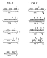
- This step is illustrated in Figure 1 of the drawings, Step A, where there is shown a substrate material 1, such as a non-conductive plastic, e.g., an epoxy circuit board base material, clad with copper cladding 2 and coated in an image pattern with organic coating material 3.
- a substrate material 1 such as a non-conductive plastic, e.g., an epoxy circuit board base material
- clad with copper cladding 2 and coated in an image pattern with organic coating material 3.
- organic coating material 3 can be accomplished in numerous ways known to the art such as by application of a screen resist or by formation of a light sensitive photoresist film over the conductive surface.
- Screen resists are organic coating conpositions that are applied to a surface through a stencil or screen to form a wet coating in an image pattern.
- the ink is hardened by baking, U.V. exposure, etc.
- Such resists typically comprise a polymer or pre-polymer binder plus initiators to cause hardening of the ink.
- Urethanes, acrylates and epoxies are typical binders for screen resists.
- Screen resists are well known in the art and disclosed in numerous publications including U.S. Patents Nos. 4,056,453; 4,104,144; 4,133,593; 4,126,527 and 4,270,985, all incorporated herein by reference. Such materials are low in cost and easy to use, but are incapable of providing images of fine line resolution.
- Photoresists are known and applied to a surface in a variety of ways such as by coating from a liquid solution, application of the resist as a dry film and by electrophoresis as described above.
- Liquid photoresists coating compositions are used to form liquid coatings from organic solutions which, when dried and exposed to light of the proper wavelength, are chemically changed in their solubility to certain solvents or developers.
- Two types are available: negative-acting and positive-acting.
- the negative acting resist is initially a mixture which is soluble in its developer but after light exposure, becomes polymerized and insoluble in developer. Exposure is made through a film pattern or master. The unexposed resist is selectively dissolved, softened or washed away leaving the desired resist pattern on the substrate.
- Positive-acting resists work in the opposite fashion: exposure to light causes the formulation to become soluble in the developer.
- the resist image is frequently dyed to make it visible for inspection and retouching.
- the resist pattern that remains after development (and post baking in some cases) is insoluble.
- Formulations for such photoresists are well known and they are typically formulated from materials such as vinyl cinnamate copolymers, as disclosed in U.S. Patent Nos. 2,737,297; 2,739,892 and 2,801,233; benzal acetophenones as disclosed in U.S. Patent Nos. 2,716,097 and 2,716,102; quaternary salts such as disclosed in U.S. Patent No. 2,908,667; azide polymers such as disclosed in U.S. Patent No. 2,948,610; and naphthoquinone diazide esters and amides as disclosed in U.S. Patent Nos. 3,634,082; 4,148,654 and 4,439,516, all
- the photoresists can also be applied in the form of a dry film as taught in U.S. Patents Nos. 4,378,264 and 4,530,896 incorporated herein by reference.
- Such dry film resists typically comprise photohardenable layers prepared from polymer binders such as polyacrylates and polyacrylate esters; monomeric components such as such as ethylenically unsaturated materials including butyl acrylate, 1,5-pentanediol diacrylate; initiators such as polynuclear quinones having two intracyclic carbon atoms in a conjugated carbocyclic ring system such as 9,10-anthraquinone; and inhibitors.
- the photoresist can be applied by electrophoretic deposition over a conductive surface. Following electrophoretic deposition of the resist coating, it is imaged and developed in conventional manner.
- the coating composition used to form the first relief image is a coating composition capable of being stripped from the surface of the substrate in a mild aqueous solution.
- a suitable negative acting resist formulation is set forth in the aforesaid U.S. Patent No. 4,378,264, Example 1, and preferably, this resist is applied as a dry film.
- a suitable positive acting photoresist is a liquid coating composition comprising a novolak type phenolic or cresol resin and a naphthoquinone diazide sulfonic acid ester in an organic solution. Compositions of this nature are disclosed in the aforesaid U.S. Patent No. 3,634,082.
- a composition exemplified by Example 2 of said patent constitutes a preferred embodment of a positive resist for use in the process of the invention.
- the next step in the process may comprise treatment of the conductive surface bared by formation of the relief image in the first organic coating.
- Such a step may involvek metal plating such as a step of copper electroplating in printed circuit manufacture.
- a step has been omitted from the process description to show the inventive process in its simplest embodiment. Additional process steps that may be applied at this point in the process will be discussed below.
- the next step in the process comprises electrophoretic deposition of a second organic coating over the exposed surface of the cladding metal bared by development and consequently not coated with the first organic layer.
- the article formed would be as shown in Step B of Figure 1 where the second coating 4 resides in the spaces between organic coating 4 which defines an image pattern over copper cladding 2.
- the first and second organic coatings are negative images of each other, and in this embodiment of the invention, clmprise a planar layer.
- the requirements of the second organic coating 4 are that it be of a material that is:
- the second organic coating is applied by electrophoretic deposition.
- the organic coating material will deposit only on the conductive surface, not on the non-conductive first organic coating. Since the first organic coating is in an image pattern, electrophoretic deposition of the second organic coating is also in an image pattern where the image pattern is a negative of the image in the first organic coating.
- conductive layer 2 as shown Figure 1 is a continuous coating providing conductivity to all areas where deposition is desired. Since the entire surface of the board is conductive, electrophoretic deposition is possible over all conductive surfaces. Therefore, the second organic coating will deposit over the bare copper, but not over those portions of the surface protected by the first organic coating which coating acts as an insulating layer preventing deposition. The result is two organic coating materials in an image pattern over a surface where one organic coating is in a negative image pattern of the other organic coating.
- the second organic coating may be a light sensitive organic coating or a light insensitive coating dependent upon the use to which the coating is put. This will be explained in greater detail below. It should be a material that will not be attacked by a solvent or stripper for the first organic coating.
- the first and second organic coatings are removable by contact with an aqueous solution where one of said organic coatings is soluble in aqueous acid solution and the other is soluble in aqueous base solution.
- Suitable electrophoretic coating compositions suitable for purposes of the second organic coating compositions are those disclosed in U.S. Patent No. 4,592,816 incorporated herein by reference. These compositions comprise aqueous solutions or emulsions of at least one polymer containing a carrier group, optionally a photoinitiator and a source of unsaturation for a crosslinking reaction if the composition is to be used as a photoresist.
- the source of unsaturation is preferably a monomer.
- the polymer component of the composition contains carrier groups that become positively or negatively charged upon contact with either an acid or a base, dependent upon the specific carrier group employed.
- the carrier group is one selected so that a deposited film will be developable with an aqueous acid or aqueous base solution.
- Suitable polymers are addition and condensation polymers having the aforesaid carrier groups. Addition polymers having carrier groups prepared from monomers having ethylenic unsaturation are preferred.
- Polymers containing carrier groups that are useful in the photosensitive polymer composition include acrylic polymers, vinyl polymers other than acrylic polymers, epoxy polymers, polyurethanes, polyesters, and polyamides.
- Polymers having positively charged carrier groups - i.e., or cataphoretic carrier groups will deposit on a negatively charged electrode.
- carrier groups include, for example, quaternary ammonium groups, sulfonium groups and sulfoxonium groups.
- Other groups which become postively charged upon reaction with an acid such as for example amine groups, may also be employed.
- the acids that are useful to protonate the carrier groups of the polymers include lactic acid, glycolic acid, hydroxyacetic acid, hydrochloric acid, formic acid, acetic acid and phosphoric acid.
- Polymers having negatively charged carrier groups - i.e., anaphoretic carrier groups, will deposit on a positively charged electrode.
- Carboxylic acid groups are suitable negatively charged carrier groups.
- the preferred compositions suitable for electrophoretic deposition are formed by mixing the polymer containing carrier groups with at least one unsaturated monomer and a photoinitiator so that a polymer film electrophoretically deposited on a surface is capable of being polymerized into a cross linked polymer when exposed to actinic radiation.
- Unsaturated monomers having two or more unsaturated groups attached to the same molecule are preferred.
- Most preferred are the multifunctional monomers having two or more acrylates or methacrylate groups attached to each monomer molecule. Examples of suitable monomers are set forth in the above referenced patent.
- photoinitiators suitable for use in the polymeric composition include the azo compounds, sulfur-containing compounds, metallic salts and complexes, oxines, amines, polynuclear compounds, organic carbonyl compounds, various quinones, etc. Specific examples of suitable photoinitiators are also set forth in U.S. Patent No. 4,592,816.
- Example 1 of U.S. Patent No. 4,592,816 is a most preferred electrophoretically depositing composition for purposes of the invention.
- compositions may also contain other additives such as wetting agents, plasticizers, coalescing agents, levelling agents, etc.
- the next step in the process involves removal of the first organic coating layer, layer 3 of Figure 1 without degrading organic coating layer 4. This is accomplished by contact of the coated surface with a solvent or stripper for the first organic coating layer which solvent is not a solvent or stripper for the second organic coating.
- a solvent or stripper for the first organic coating layer which solvent is not a solvent or stripper for the second organic coating.
- both organic coating layer 3 and layer 4 are soluble in a mild aqueous acid or base solution provided both are not soluble in the same solvent.
- the composite would have the structure shown in Step C of Figure 1 comprising substrate 1, copper cladding 2, and organic coating layer 4.
- the next step in the process comprises the permanent alteration of the surface bared by removal of the first organic coating layer.
- Permanent alteration of the surface can comprise addition of a substance to the surface or removal of a portion or all of the surface.
- Addition to the surface can be by deposition of metal onto the surface. Removal of the surface can be by etching.
- a procedure involving deposition would result in the structure depicted in Step D of Figure 1 where layer 5 illustrates a deposited material such as a metal.
- Etching of the surface would result in the structure depicted in Step E of Figure 1 where the underlaying surface 2 bared by removal of the first organic layer 3 has been removed by contact with an etchant.
- an intermediate article formed in the process of the invention is similar to an intermediate article formed using a photoresist alone.
- a photoresist With a photoresist, a surface is coated with the photoresist and following exposure to activating radiation, the coating has areas of differing solubility.
- the exposed photoresist coating is an organic coating with discrete areas of differing solubility. This is similar to the coating formed by the process of the subject invention as depicted in Step B of Figure 1.
- the organic coating of the subject invention is formed subsequently to the development of an exposed photoresist layer and provides a coating having greater flexibility than an organic coating comprising an exposed and undeveloped photoresist.
- the electrophoretically deposited coating is able to withstand aggressive chemical environments that a photoresist would be unable to withstand.
- the negative acting photoresist would be unable to withstand high temperature alkaline solutions such as the solutions used for immersion plating of gold.
- the preferred electrophoretically deposited coatings would be able to withstand such solutions.
- Step A of Figure 2 shows a printed circuit board base material comprising a dielectric substrate 10 and copper cladding 11.
- the board may have plated through-holes (not shown in the drawing) if desired.
- a photoresist coating is applied over the circuit board base material, imaged and developed to yield relief image 12.
- electroplated copper 13 is deposited over copper not coated with relief image 12. As shown, the copper is deposited in a thickness equivalent to the height of relief image 12. This is not a requirement of the process.
- Step C of Figure 2 The next step in the process, illustrated as Step C of Figure 2, comprises electrophoretic deposition of the second organic coating 14 over electroplated copper 13.
- Organic coating 14 will deposit only over a conductive surface and therefore deposits in a negative image of organic coating 12.
- organic coatings 12 and 14 form a single layer which is non-planar i.e., of differing heights.
- Step D of Figure 2 The final steps of the process are shown by Step D of Figure 2. These steps involve preferential removal of organic coating 12 and etching or bared copper layer 11 to provide an article comprising substrate 10 having conductor lines comprising cladding layer 11 reinforced with electrolytic copper layer 13 protected by the electrophoretically deposited coating layer 14.
- a process substituting an electrophoretically deposited organic coating as an etch resist for an electroplated dissimilar metal etch resist such as solder is an improvement in the art. Electroplating solder to full thickness sufficient to act as an etch resist is time consuming and lowers the through put in the manufacture of printed circuit boards. The process of stripping the solder from the board is time consuming, involves etchants that are difficult to handle and leaves a waste solution which requires expensive wste treatment procedures for disposal.
- a process for manufacture of a printed circuit board substituting an electrophoretically deposited organic coating for electrolytic deposited dissimilar metal is more specifically described in the following Example which represents the most preferred embodiment of the invention.
- a circuit board material was used that was received with plated through holes, an imaged and developed negative dry film coating and an electroplated copper deposit over the copper bared by development of the negative dry film.
- the procedures for forming a circuit board base material of this nature are known in the art and do not, by themselves, constitute a part of this invention. Therefore, Steps 1 through 4 that follow are hypothetical and are intended to illustrate a manner in which the circuit board base material may be prepared.
- Step 1 Prepare a printed circuit board base material for further processing.
- the circuit board base material used is an FR-4 laminate coated on both sides with copper.
- the board could be prepared by a sequence of steps including drilling through holes at appropriate locations, cleaning the copper for further processing, catalyzing the board with a tin-palladium colloid such as the catalyst sold under the tradename Cataposit 44 by Shipley Company Inc. of Newton, Mass. and electroplating copper onto the walls of the through holes and onto the copper cladding.
- An electroless copper plating solution such as that sold under the tradename CP-78, also available from Shipley Company Inc., would be suitable for the deposition step. Times of immersion and conditions would be in accordance with the instructions supplied by the manufacturer of the materials used.
- Step 2 Apply photoresist film to circuit board base material with plated through holes.
- a negative dry film photoresist would be applied to the circuit board base material prepared in accordance with the procedure of Step 1.
- the film used would preferably be one sold under the trademark Riston, a negative acting dry film available from E. I. Dupont de Nemours and Co. of Wilmington, Delaware. Heat and pressure would be used to apply the film to the board. Conditions for application of the film would be in accordance with instructions from the manufacturer of the film.
- Step 3 Expose and develop photoresist.
- the board coated with the negative dry film would be exposed through a master in a desired image pattern to a source of activating radiation and developed with either a weak carbonate solution or a commercial developer available for the Riston dry film resists. Exposure and development would be in accordance with instructions from the manufacturer of the film.
- Step 4 Electroplate copper.
- electroless copper deposit would be reinforced by a deposit of electrolytic copper.
- a suitable electrolytic copper depositing solution would be Electroposit 892 available from Shipley Company Inc. Conditions such as current density, deposition temperature, etc. would be in accordance with instructions from Shipley Company Inc.
- Step 5 Electrophoretically deposit organic coating over copper.
- the electrophoretic depositing composition used was as follows: Polymer 132.0 grams Dimethylamino ethyl methacrylate (8 parts) Methyl methacrylate (68 parts) Butyl acrylate (23 parts) Vinyl acetate (1 part) Trimethylolpropane triacrylate 46.0 grams Dye* 1.6 grams Acetone 12.0 grams Lactic acid (20%) 24.0 grams Distilled water to 1000.0 grams * Orasol Blue 2GLN available from Ciba Geigy Chemical Company.
- a portion of the above composition was added to a 250 ml. beaker used as a plating cell.
- a 1" x 2" Monel screen was used as the anode and the circuit board base material was used as the cathode.
- the anode to cathode space was 2 inches.
- Bath temperature was maintained at 22°C.
- a voltage of 60 volts was applied across the electrodes and the voltage was applied for 10 seconds which was sufficient to deposit the electrophoretic coating over the copper electroplate.
- Step 6 Strip photoresist from circuit board base material.
- the Riston photoresist was removed by immersion of the circuit board base material in a 2% solution of potassium hydroxide maintained at 60°C for 60 seconds.
- Copper bared by removal of the photoresist film was removed by etching with a cupric chloride etchant for a time sufficient to remove all exposed copper.
- Step 8 Remove electrophoretic coating.
- the electrophoretic coating was removed by immersion in a 5% lactic acid solution until all of the coating was removed.
- the electrophoretically deposited coating need not be a photosensitive coating.
- electrophoretic coatings that are light sensitve photoresist compositions.
- electrophoretically deposited photoresists in the process of the invention would permit additional commercial uses.
- an electrophoretically deposited photoresist could find application in the above process for manufacture of circuit boards where prior to the step of removal of the dry film photoresist, the remaining electrophoretically applied resist could be blanket exposed to cure the same. This exposure would result in the coating providing even better resistance to aggressive environments than the uncured coating.
- a connector is attached to the circuit by sliding the connector onto conductive tabs located on the edge of the circuit board. These tabs must be hard and oxidation resistant. To obtain hardness and oxidation resistance, the tabs are conventionally plated first with electroplated nickel and then with electroplated gold.
- platers tape would be placed directly above the tabs to isolate the tabs from the balance of the board. Solder would then be stripped from the tabs and the tabs plated first with nickel and then with gold.
- This process can be greatly simplified using an electrophoretically deposited light sensitive coating of the type described above.
- the electrophoretically deposited coating would be imaged in a band above the tabs to cure the same. The remainder of the coating would then be removed by development to expose the tabs for plating. The process would avoid the need for platers tape.
- the following example illustrates such a process and represents an additional preferred embodiment of the invention.
- tab plating was not actually performed and the method of tab plating would be in accordance with prior art procedures.
- Step 5 from example 1 The procedure of Step 5 from example 1 is repeated, but a photoinitiator is added to the formulation of the electrophoretic coating composition.
- the photoinitiator used is Darocur 1664, a mixture of acrylic ketones commercially available from Merck Chemical Company.
- the photoinitiator is used in an amount of 4.0 grams per 1000 grams of the formulation.
- the electrophoretically deposited photoresist is exposed through a master in the form of a band above the areas of the tabs.
- the method of exposure comprises exposure to a mercury light source at an exposure energy of 200 mJ/cm2. Development is by immersion in 5% aqueous solution of lactic acid at 25°C for 60 seconds.
Landscapes
- Engineering & Computer Science (AREA)
- Manufacturing & Machinery (AREA)
- Microelectronics & Electronic Packaging (AREA)
- Physics & Mathematics (AREA)
- General Physics & Mathematics (AREA)
- Manufacturing Of Printed Circuit Boards (AREA)
- Manufacturing Of Printed Wiring (AREA)
Applications Claiming Priority (2)
| Application Number | Priority Date | Filing Date | Title |
|---|---|---|---|
| US891609 | 1986-08-01 | ||
| US06/891,609 US4751172A (en) | 1986-08-01 | 1986-08-01 | Process for forming metal images |
Publications (2)
| Publication Number | Publication Date |
|---|---|
| EP0255557A2 true EP0255557A2 (fr) | 1988-02-10 |
| EP0255557A3 EP0255557A3 (fr) | 1988-08-10 |
Family
ID=25398517
Family Applications (1)
| Application Number | Title | Priority Date | Filing Date |
|---|---|---|---|
| EP86112660A Withdrawn EP0255557A3 (fr) | 1986-08-01 | 1986-09-12 | Procédé de formation d'images métalliques |
Country Status (3)
| Country | Link |
|---|---|
| US (1) | US4751172A (fr) |
| EP (1) | EP0255557A3 (fr) |
| JP (1) | JPS63146485A (fr) |
Cited By (7)
| Publication number | Priority date | Publication date | Assignee | Title |
|---|---|---|---|---|
| EP0261301A3 (fr) * | 1986-09-22 | 1988-08-03 | Ube Industries, Ltd. | Procédé de fabrication d'une plaque de circuit imprimé comportant des trous métallisés en travers |
| EP0250366A3 (fr) * | 1986-06-18 | 1990-02-07 | Ciba-Geigy Ag | Méthode de production de structures métalliques |
| EP0349161A3 (en) * | 1988-06-27 | 1990-05-09 | American Telephone And Telegraph Company | Printed wiring board fabrication method |
| US5073478A (en) * | 1988-11-29 | 1991-12-17 | Ciba-Geigy Corporation | Method of making a pattern |
| EP0472210A3 (fr) * | 1990-08-23 | 1992-03-25 | Nippon Paint Co., Ltd. | Procédé de production d'un filtre en couleurs |
| EP0517400A1 (fr) * | 1991-06-05 | 1992-12-09 | Macdermid Incorporated | Procédé de fabrication de circuits imprimés utilisant des réserves organiques déposées par électrophorèse |
| EP0528484A1 (fr) * | 1991-08-14 | 1993-02-24 | Koninklijke Philips Electronics N.V. | Procédé pour déposer une pâte pour un actionneur céramique à couches multiples |
Families Citing this family (27)
| Publication number | Priority date | Publication date | Assignee | Title |
|---|---|---|---|---|
| WO1988005924A1 (fr) * | 1987-01-28 | 1988-08-11 | Nissha Printing Co., Ltd. | Filtre colore et procede de fabrication |
| JPS63246890A (ja) * | 1987-04-02 | 1988-10-13 | 関西ペイント株式会社 | プリント回路の形成方法 |
| JPS6420694A (en) * | 1987-07-15 | 1989-01-24 | Kansai Paint Co Ltd | Manufacture of printed wiring board |
| GB8801736D0 (en) * | 1988-01-27 | 1988-02-24 | Ciba Geigy Ag | Method of making patterns |
| JPH0234984A (ja) * | 1988-04-13 | 1990-02-05 | Mitsubishi Electric Corp | プリント回路基板の製造方法 |
| GB8913090D0 (en) * | 1989-06-07 | 1989-07-26 | Ciba Geigy Ag | Method |
| US5004672A (en) * | 1989-07-10 | 1991-04-02 | Shipley Company Inc. | Electrophoretic method for applying photoresist to three dimensional circuit board substrate |
| US5234558A (en) * | 1990-03-22 | 1993-08-10 | Canon Kabushiki Kaisha | Electrically conductive circuit member, method of manufacturing the same and electrically conductive paste |
| US5055164A (en) * | 1990-03-26 | 1991-10-08 | Shipley Company Inc. | Electrodepositable photoresists for manufacture of hybrid circuit boards |
| CA2048164C (fr) * | 1990-08-02 | 1998-11-10 | Kurt G. Olson | Resine photosensible de photo-imagerie a electrodeposition |
| US5268256A (en) * | 1990-08-02 | 1993-12-07 | Ppg Industries, Inc. | Photoimageable electrodepositable photoresist composition for producing non-tacky films |
| US5202222A (en) * | 1991-03-01 | 1993-04-13 | Shipley Company Inc. | Selective and precise etching and plating of conductive substrates |
| US5288377A (en) * | 1991-06-05 | 1994-02-22 | Macdermid, Incorporated | Process for the manufacture of printed circuits using electrophoretically deposited organic resists |
| US5160579A (en) * | 1991-06-05 | 1992-11-03 | Macdermid, Incorporated | Process for manufacturing printed circuit employing selective provision of solderable coating |
| DE69329249T2 (de) * | 1993-01-11 | 2001-02-01 | Macdermid, Inc. | Phosphatisierungsverfahren, insbesondere für die herstellung von leiterplatten und verwendung organischer rückstände |
| US6153075A (en) | 1998-02-26 | 2000-11-28 | Micron Technology, Inc. | Methods using electrophoretically deposited patternable material |
| US6048445A (en) * | 1998-03-24 | 2000-04-11 | Intel Corporation | Method of forming a metal line utilizing electroplating |
| US6319381B1 (en) | 1998-06-11 | 2001-11-20 | Micron Technology, Inc. | Methods of forming a face plate assembly of a color display |
| US6383720B1 (en) * | 1998-08-18 | 2002-05-07 | Matsushita Electric Industrial Co., Ltd. | Method of manufacturing fine pattern and printed circuit board manufactured with this method |
| US5928435A (en) * | 1998-11-11 | 1999-07-27 | Enthone-Omi, Inc. | Method for removing organic coatings from substrates using carboxylic acids, organic solvents, and corrosion inhibitors |
| US6503564B1 (en) * | 1999-02-26 | 2003-01-07 | 3M Innovative Properties Company | Method of coating microstructured substrates with polymeric layer(s), allowing preservation of surface feature profile |
| US6536477B1 (en) * | 2000-10-12 | 2003-03-25 | Nanostream, Inc. | Fluidic couplers and modular microfluidic systems |
| US6887651B2 (en) * | 2002-11-25 | 2005-05-03 | International Business Machines Corporation | Electrodeposited photoresist and dry film photoresist photolithography process for printed circuit board patterning |
| US7095122B2 (en) * | 2004-09-01 | 2006-08-22 | Micron Technology, Inc. | Reduced-dimension microelectronic component assemblies with wire bonds and methods of making same |
| CN101144967B (zh) * | 2007-06-28 | 2011-04-06 | 武汉立胜超滤科技发展有限公司 | 正性电泳涂料在印制板的图形转移上的电泳涂装方法及成套设备 |
| EP2602360A1 (fr) * | 2011-12-06 | 2013-06-12 | Grundfos Holding A/S | Procédé d'application d'une marque distinctive sur un corps métallique |
| CN106471158B (zh) * | 2014-06-23 | 2019-05-31 | 惠普发展公司有限责任合伙企业 | 制造多层涂层的方法以及涂覆的基材 |
Family Cites Families (7)
| Publication number | Priority date | Publication date | Assignee | Title |
|---|---|---|---|---|
| GB1194826A (en) * | 1966-08-09 | 1970-06-10 | Ronson Products Ltd | Improvements relating to Electro-Plating and Etching Processes |
| US3892646A (en) * | 1970-08-17 | 1975-07-01 | Ibm | Process for selectively forming electrophoretic coatings on electrical contacts |
| US4170819A (en) * | 1978-04-10 | 1979-10-16 | International Business Machines Corporation | Method of making conductive via holes in printed circuit boards |
| GB1562179A (en) * | 1978-04-11 | 1980-03-05 | Standard Telephones Cables Ltd | Electroplating |
| EP0155231B2 (fr) * | 1984-03-07 | 1997-01-15 | Ciba-Geigy Ag | Procédé pour réaliser des images |
| DE3435158C1 (de) * | 1984-09-25 | 1986-04-17 | Siemens AG, 1000 Berlin und 8000 München | Verfahren zum Beschichten von kupferkaschierten Leiterplatten |
| US4592816A (en) * | 1984-09-26 | 1986-06-03 | Rohm And Haas Company | Electrophoretic deposition process |
-
1986
- 1986-08-01 US US06/891,609 patent/US4751172A/en not_active Expired - Fee Related
- 1986-09-12 EP EP86112660A patent/EP0255557A3/fr not_active Withdrawn
-
1987
- 1987-06-12 JP JP62146850A patent/JPS63146485A/ja active Pending
Cited By (8)
| Publication number | Priority date | Publication date | Assignee | Title |
|---|---|---|---|---|
| EP0250366A3 (fr) * | 1986-06-18 | 1990-02-07 | Ciba-Geigy Ag | Méthode de production de structures métalliques |
| EP0261301A3 (fr) * | 1986-09-22 | 1988-08-03 | Ube Industries, Ltd. | Procédé de fabrication d'une plaque de circuit imprimé comportant des trous métallisés en travers |
| EP0349161A3 (en) * | 1988-06-27 | 1990-05-09 | American Telephone And Telegraph Company | Printed wiring board fabrication method |
| US5073478A (en) * | 1988-11-29 | 1991-12-17 | Ciba-Geigy Corporation | Method of making a pattern |
| EP0472210A3 (fr) * | 1990-08-23 | 1992-03-25 | Nippon Paint Co., Ltd. | Procédé de production d'un filtre en couleurs |
| US5186801A (en) * | 1990-08-23 | 1993-02-16 | Nippon Paint Co., Ltd. | Production of color filter |
| EP0517400A1 (fr) * | 1991-06-05 | 1992-12-09 | Macdermid Incorporated | Procédé de fabrication de circuits imprimés utilisant des réserves organiques déposées par électrophorèse |
| EP0528484A1 (fr) * | 1991-08-14 | 1993-02-24 | Koninklijke Philips Electronics N.V. | Procédé pour déposer une pâte pour un actionneur céramique à couches multiples |
Also Published As
| Publication number | Publication date |
|---|---|
| EP0255557A3 (fr) | 1988-08-10 |
| JPS63146485A (ja) | 1988-06-18 |
| US4751172A (en) | 1988-06-14 |
Similar Documents
| Publication | Publication Date | Title |
|---|---|---|
| US4751172A (en) | Process for forming metal images | |
| US5004672A (en) | Electrophoretic method for applying photoresist to three dimensional circuit board substrate | |
| US4576902A (en) | Process of making and using a positive working photosensitive film resist material | |
| KR920007122B1 (ko) | 회로판의 제조방법 | |
| US4746399A (en) | Method for making metallic patterns | |
| US4804615A (en) | Method for manufacture of printed circuit boards | |
| KR930010060B1 (ko) | 땜납도금회로와 관통공을 갖는 인쇄회로판의 제조방법 | |
| US5314789A (en) | Method of forming a relief image comprising amphoteric compositions | |
| JPH0456976B2 (fr) | ||
| US5202222A (en) | Selective and precise etching and plating of conductive substrates | |
| US3240684A (en) | Method of etching rhodium plated metal layers and of making rhodium plated printed circuit boards | |
| US4690833A (en) | Providing circuit lines on a substrate | |
| JP3039746B2 (ja) | 印刷配線板の製造法 | |
| KR100735659B1 (ko) | 요판 옵셋용 마스터 판, 그 마스터 판의 제조방법 및 그마스터 판을 이용한 막(膜)회로의 형성방법 | |
| DE3814566C1 (fr) | ||
| CA2067921A1 (fr) | Nouvelle methode de fabrication de circuits electriques | |
| JPS63310196A (ja) | 金属パターンの形成方法 | |
| US7635552B2 (en) | Photoresist composition with antibacterial agent | |
| EP0449022A2 (fr) | Procédé pour contrôler l'épaisseur d'un film photorésist et la stabilité d'un bain d'électrodéposition | |
| DE4339019A1 (de) | Verfahren zur Herstellung von Leiterplatten | |
| JPS58100493A (ja) | スルホ−ルプリント配線基板の製造法 | |
| JPS58166793A (ja) | プリント回路板の製造法 | |
| KR20000047683A (ko) | 레지스트층의 형성방법 및 프린트 배선기판의 제조방법 | |
| JPS5974693A (ja) | スルホ−ル配線基板の製造方法 | |
| JPS60236284A (ja) | 印刷配線板の製造方法 |
Legal Events
| Date | Code | Title | Description |
|---|---|---|---|
| PUAI | Public reference made under article 153(3) epc to a published international application that has entered the european phase |
Free format text: ORIGINAL CODE: 0009012 |
|
| AK | Designated contracting states |
Kind code of ref document: A2 Designated state(s): AT BE CH DE FR GB IT LI LU NL SE |
|
| PUAL | Search report despatched |
Free format text: ORIGINAL CODE: 0009013 |
|
| AK | Designated contracting states |
Kind code of ref document: A3 Designated state(s): AT BE CH DE FR GB IT LI LU NL SE |
|
| 17P | Request for examination filed |
Effective date: 19881213 |
|
| 17Q | First examination report despatched |
Effective date: 19910326 |
|
| STAA | Information on the status of an ep patent application or granted ep patent |
Free format text: STATUS: THE APPLICATION IS DEEMED TO BE WITHDRAWN |
|
| 18D | Application deemed to be withdrawn |
Effective date: 19931002 |
|
| RIN1 | Information on inventor provided before grant (corrected) |
Inventor name: HAWKINS, ROBERT E. Inventor name: RODRIQUEZ, STEPHEN S. |