EP0256324A1 - Circuit de mesure de la conductivité - Google Patents
Circuit de mesure de la conductivité Download PDFInfo
- Publication number
- EP0256324A1 EP0256324A1 EP87110412A EP87110412A EP0256324A1 EP 0256324 A1 EP0256324 A1 EP 0256324A1 EP 87110412 A EP87110412 A EP 87110412A EP 87110412 A EP87110412 A EP 87110412A EP 0256324 A1 EP0256324 A1 EP 0256324A1
- Authority
- EP
- European Patent Office
- Prior art keywords
- circuit
- cell
- converter
- input terminals
- voltage
- Prior art date
- Legal status (The legal status is an assumption and is not a legal conclusion. Google has not performed a legal analysis and makes no representation as to the accuracy of the status listed.)
- Withdrawn
Links
- 239000003990 capacitor Substances 0.000 claims abstract description 20
- 238000006243 chemical reaction Methods 0.000 claims abstract description 19
- 238000005070 sampling Methods 0.000 claims abstract description 11
- 230000009977 dual effect Effects 0.000 claims abstract description 4
- 238000005259 measurement Methods 0.000 claims description 15
- 230000010354 integration Effects 0.000 claims description 9
- 230000010287 polarization Effects 0.000 claims description 4
- 230000001419 dependent effect Effects 0.000 claims 1
- 230000000694 effects Effects 0.000 abstract 1
- 238000010586 diagram Methods 0.000 description 7
- 238000001514 detection method Methods 0.000 description 3
- 238000000034 method Methods 0.000 description 3
- 239000007787 solid Substances 0.000 description 3
- 239000007788 liquid Substances 0.000 description 1
- 239000004973 liquid crystal related substance Substances 0.000 description 1
- 239000004065 semiconductor Substances 0.000 description 1
- 230000001360 synchronised effect Effects 0.000 description 1
Images


Classifications
-
- G—PHYSICS
- G01—MEASURING; TESTING
- G01N—INVESTIGATING OR ANALYSING MATERIALS BY DETERMINING THEIR CHEMICAL OR PHYSICAL PROPERTIES
- G01N27/00—Investigating or analysing materials by the use of electric, electrochemical, or magnetic means
- G01N27/02—Investigating or analysing materials by the use of electric, electrochemical, or magnetic means by investigating impedance
- G01N27/04—Investigating or analysing materials by the use of electric, electrochemical, or magnetic means by investigating impedance by investigating resistance
- G01N27/06—Investigating or analysing materials by the use of electric, electrochemical, or magnetic means by investigating impedance by investigating resistance of a liquid
-
- G—PHYSICS
- G01—MEASURING; TESTING
- G01N—INVESTIGATING OR ANALYSING MATERIALS BY DETERMINING THEIR CHEMICAL OR PHYSICAL PROPERTIES
- G01N27/00—Investigating or analysing materials by the use of electric, electrochemical, or magnetic means
- G01N27/02—Investigating or analysing materials by the use of electric, electrochemical, or magnetic means by investigating impedance
- G01N27/04—Investigating or analysing materials by the use of electric, electrochemical, or magnetic means by investigating impedance by investigating resistance
- G01N27/045—Circuits
-
- G—PHYSICS
- G01—MEASURING; TESTING
- G01R—MEASURING ELECTRIC VARIABLES; MEASURING MAGNETIC VARIABLES
- G01R27/00—Arrangements for measuring resistance, reactance, impedance, or electric characteristics derived therefrom
- G01R27/02—Measuring real or complex resistance, reactance, impedance, or other two-pole characteristics derived therefrom, e.g. time constant
- G01R27/22—Measuring resistance of fluids
Definitions
- a conductivity measuring circuit for measuring the conductivity of a solution.
- This circuit includes an analog-to-digital converter for producing a digital output indicative of the analog voltage drop across its signal input terminals.
- the voltage drop is provided by pair of electrodes immersed in the solution to be measured and is sampled before each conversion cycle by a capacitor associated with the converter. The sampling is timed by the converter clock in a manner such that the capacitor is always fully charged in the proper polarity at the end of the sampling period.
- the capacitor then provides the input to be converted by the converter.
- the electrodes are connected to a source of ac current that is synchronized with the clock of the analog-to-digital converter.
- a pair of current input terminals are provided in conjunction with a switching circuit so as to connect the current input terminals to the electrodes through the switching circuit alternately in one sense and then the other.
- the current input terminals connected in series circuit with a known resistance and a source of dc voltage, their is provided the source of known ac current for the electrodes.
- the current is known because the known resistance is connected across the reference input of the converter so that integration in one phase of the conversion process is in response to the drop across the known resistance.
- the voltage drop across the electrodes can be connected to the signal input of the converter either directly or through the switch, as by connecting the converter signal input to the current input terminals instead of directly to the electrodes.
- Fig. 1 there is shown a prior art circuit which can be used to measure the conductivity of an element, such as the unknown resistor R x .
- This is accomplished by a ratiometric measurement, whereby the unknown resistance is measured with respect to a known standard resistance, R std .
- This method requires no accurately defined reference voltage or current. Instead it uses a commom current passing through both a standard and an unknown resistance in order to develop across the unknown, R x , a voltage which can be applied to one differential input of an analog-to-digital converter 50 (shown as a 7126, for example) as the signal or unknown input and another voltage across the standard, R std , which can be applied to the other differential input of the converter as the reference or known input.
- an analog-to-digital converter 50 shown as a 7126, for example
- the converter will produce an output to the display which will give a display reading of (1000)R std /R x in the units of mhos.
- R std the voltage drop across the known resistance will be supplied to the terminals REF HI and REF LO, with the drop across the unknown supplied to the terminals, IN HIGH and IN LO (this being the normal orientation for the terminals, their names are properly descriptive).
- Fig. 2a shows the analog section of a single chip CMOS TSC7126 as manufactured by Teledyne Semiconductor and illustrated on page 7-73 of their Data Acquisition Design Handbook of 1984.
- This drawing shows the typical elements of a dual-slope integrating analog-to-digital converter having two differential inputs along with the necessary external components which must be added to cause it to operate as desired.
- the external or auxilliary circuitry of Figs. 2a and 2b required to operate the 7126, will be considered a part of the 7126 when it is shown in subsequent drawings.
- reference to an integrated analog-to-digital converter shall be considered to include the necessary external circuitry for operation as a converter unless the external circutry is specifically described.
- the conventional dual-slope converter measurement cycle has two distinct phases: the input signal integration and the reference voltage integration (deintegration).
- the input signal being converted is integrated for a fixed time period. Time is measured by counting clock pulses. An opposite polarity, constant reference voltage is then integrated until the integrator output voltage returns to zero. The reference integration time, as measured by the clock, is then proportional to the input signal.
- Fig. 2a incorporates and auto-zero cycle.
- This cycle removes buffer amplifier, intergrator, and comparator offset voltage error terms from the conversion.
- a true digital zero reading results without external adjusting potentiometers.
- a complete conversion will then consist of three cycles: an auto-zero, signal integrate and reference integrate (deintegrate) cycle.
- the differential input signal is disconnected from the circuit by opening internal analog gates.
- the internal nodes are shorted to analog common (ground) to establish a zero input condition.
- Additional analog gates close a feedback loop around the integrator and comparator. This loop permits comparator offset voltage error compensation.
- the voltage level established on capacitor C az compensates for device offset voltages.
- the auto-zero loop is opened and the internal differential inputs connect to V in + and V in ⁇ .
- the differential input signal is integrated for a fixed time period (1000 counts).
- the externally set clock frequency is divided by four before clocking the internal counters.
- the final phase is reference integrate or deintegrate.
- V in ⁇ is internally connected to analog common and V in + is connected across the previously charged reference capacitor C ref .
- Circuitry within the chip ensures that the capacitor will be connected with the correct polarity to cause the integrator output to return to zero.
- the time required for the output to return to zero is proportional to the input signal and is between 0 and 2000 internal clock periods.
- the digital reading displayed is 1000 (V in /V ref ).
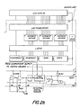
- the digital seciton of the same 7126 integrated package is shown in Fig. 2b. It contains all the segment drivers necessary to drive a 3-1/2 digit liquid crystal display.
- An LCD backplane driver is included.
- the backplane frequency is the external clock frequency divided by 800. For three conversions/sec. the backplane frequency is 60 Hz with a 5 volt nominal amplitude.
- the frequency of the clock of the 7126 is determined by the RC network which uses the three pins, 38, 39, and 40.
- This network includes R osc connected between pins 39 and 40 and C osc connected between pins 38 and 40.
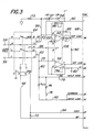
- Fig. 3 is a circuit diagram of one form of my invention which allows that to be accomplished.
- Fig. 3 the conductivity of a solution is a conductivity cell (not shown) is measured by connecting the cell across cell input terminals 54 and 56.
- the voltage across resistor 55 which is slightly less than V+ (by the drop across the two diodes 57 and 58) is connected through a first circuit (leads 59 and 60) across a series circuit including current input terminals 61 and 62 and the known resistance element R std .
- the fact that the current flow will vary with changes in conductivity of the solution in the cell will, of course, be of no importance in this circuit since the current through the cell and R std will always be the same. That current may be considered to be a known dc current since the drop across the know resistance is supplied as a known input to the converter.
- the cell input terminals are connected to the current input terminals by a switching circuit which includes switch means 64 for connecting the current input terminals alternately to the cell terminals in one sense, or polarity, and then in the other sense at a rate of actuation sufficient to prevent polarization of the cell by the dc applied to the current input terminals.
- the switch means 64 as shown in Fig. 3, may be a type 303 switch, such as can be purchased from Harris. This switch is driven by an ac signal on line 66, which is shown as the backplane signal from a 7126 type analog-to-digital converter 68 which may be operating at a frequency of 44 Hz, for example.
- pins 2 and 3 are connected and pins 12 and 13 are connected so as to connect the cell terminal 54 to current input terminal 61 and cell terminal 56 to current input terminal 62, all of which makes the terminal 54 positive.
- the connections of the cell input terminals to the current input terminals are reversed and the terminal 54 is negative, since it is connected to terminal 62 through the connection of pins 10 and 11 by the switch.
- Terminal 56 is then positive by way of its connection to terminal 61 through connection of pins 4 and 5 by the switch.
- the standard resistance, R std is arranged to be paralleled by a second standard resistance 74 when switch 76 is closed.
- the purpose of resistor 76 is to provide a decade change in range for the circuit.
- the standard resistance and its parallel resistance 74 when used, is connected as the reference input across the remaining differential input, INPUT HIGH and INPUT LOW (at pins 31 and 30, respectively), of the converter 68 by leads 78 and 80.
- the common terminal of the converter, pin 32 is made common with the INPUT LOW terminal, 30.
- the positive side of the voltage supply is connected to the converter 68, at pin 1, by way of lead 82, and the ground side is connected by lead 83 to pin 26 of the converter.
- the ground connection for the switch 64, pin 7, is connected to digital ground for the converter at pin 37, which is labelled TEST, by lead 84.
- the positive side of the voltage supply to the switch is to pin 14 by way of leads 82 and 86.
- resistors 88 and 90 can advantageously have values of 41.2K and 5.25K, respectively.
- resistors 88 and 90 can advantageously have values of 41.2K and 5.25K, respectively.
- the divider In order to prevent the voltage divider from loading the cell, it is important to make the divider look like a high impedance circuit to the cell. This is done by interposing operational amplifiers in the leads 70 and 72 as part of the tempature compensating network.
- lead 70 is connected to the noninverting input amplifier 92 to produce a potential at its output which is applied to one side of the temperature compensating circuit.
- the lead 72 from current terminal 62 connects to the noninverting input of amplifier 94, which produces at its output the input to the other side of the temperature compensating circuit and the REF LOW input of the converter at pin 35.
- the negative feedback for amplifier 94 is by way of lead 96 so that the inverting input is connected directly to the amplifier output making the amplifier a follower in that its output signal follows its input signal.
- the negative feedback is by way of variable resistor 98 to the inverting input of the amplifier, which input is also connected to the output of amplifier 94 by way of resistor 100.
- the resistors 98 and 100 form a voltage divider which varies the part of the output of 92 which is fed back to its inverting input in accordance with the setting of resistor 98.
- the output of amplifier 92 will then be maintained at a level sufficient to keep the input to its inverting input at the same level as the input to the noninverting input, representative of the cell drop.
- Variable resistor 98 therefore, provides a means for calibrating the circuit.
- the two amplifiers 92 and 94 can be a package 102, such as a 7621, shown with the dashed lines enclosing the amplifiers.
- the positive of the voltage supply for the package can be supplied to it pin 8 by lead 86, whereas the ground connection can be supplied by way of lead 83 to pin 4.
- the connections between the converter signal input terminals 35 and 36 and the cell input terminals can be by way of leads 70a and 72a (instead of through the switching element), the temperature compensating network, and the associated amplifiers, as shown in Fig. 4.
- Fig. 4 differs from Fig. 3 only in the addition of leads 70a and 72a and the ommission of leads 70 and 72.
- One cell input terminal 54 is connected by lead 70a to the noninverting input of amplifier 92 and the other cell input terminal 56 is connecter by the lead 72a to the noninverting input of amplifier 94.
- Fig. 4 With the arrangement of Fig. 4 it is possible to use cell constants that are lower than those needed for the ciruit of Fig. 3.
- the cell constant can be 1, for example, when using the circuit of Fig. 4. Better accuracy and wider ranges for conductivity measurements are other benefits realized by use of the circuit of Fig. 4.
- solid state analog-to-digital converters other than the 7126 can be used. It is only necessary that they have differential inputs and a sampling capacitor associated with the reference input. Likewise, switching elements other than the 303 can be used and the operational amplifiers can be provided without limiting one's choice to the 7621 mentioned. It will also be evident to those of ordinary skill in this art that ac current sources may be obtained by means other than by switching a dc current source, as illustrated in this description. It will further be evident that resistance measurements can be made instead of conductivity by merely reversing the input connections as pointed out in connection with Fig. 1, as long as the capacitor sampling is done on the unknown input when ac is being sampled. Alternatively, of course, the output can be inverted. Such variations are meant to be within the scope of equivalents covered by the claims.
- the unknown input signal to the analog-to-digital converter will be referred to as the signal input and will be referred to as being connected to terminals identified as signal input terminals, regardless of the nomenclature used by the manufacturers in connection with those terminals on integrated circuit packages.
- the manufacturers nomenclature is shown in the drawings.
- the known input to the converter will be referred to as the reference input and the terminals to which it is connected will be referred to as the reference input terminals, regardless of the manufacturers nomenclature.
Landscapes
- Chemical & Material Sciences (AREA)
- Physics & Mathematics (AREA)
- General Physics & Mathematics (AREA)
- Life Sciences & Earth Sciences (AREA)
- Electrochemistry (AREA)
- Health & Medical Sciences (AREA)
- Chemical Kinetics & Catalysis (AREA)
- Analytical Chemistry (AREA)
- Biochemistry (AREA)
- General Health & Medical Sciences (AREA)
- Immunology (AREA)
- Pathology (AREA)
- Measurement Of Resistance Or Impedance (AREA)
- Investigating Or Analyzing Materials By The Use Of Electric Means (AREA)
Applications Claiming Priority (2)
| Application Number | Priority Date | Filing Date | Title |
|---|---|---|---|
| US06/889,033 US4786875A (en) | 1986-07-22 | 1986-07-22 | Conductivity measuring circuit |
| US889033 | 1986-07-22 |
Publications (1)
| Publication Number | Publication Date |
|---|---|
| EP0256324A1 true EP0256324A1 (fr) | 1988-02-24 |
Family
ID=25394388
Family Applications (1)
| Application Number | Title | Priority Date | Filing Date |
|---|---|---|---|
| EP87110412A Withdrawn EP0256324A1 (fr) | 1986-07-22 | 1987-07-17 | Circuit de mesure de la conductivité |
Country Status (3)
| Country | Link |
|---|---|
| US (1) | US4786875A (fr) |
| EP (1) | EP0256324A1 (fr) |
| JP (1) | JPH0644025B2 (fr) |
Cited By (3)
| Publication number | Priority date | Publication date | Assignee | Title |
|---|---|---|---|---|
| EP0412746A3 (en) * | 1989-08-08 | 1991-07-24 | Lawrence W. Klein | Fluid testing device and method |
| WO1997044660A1 (fr) * | 1996-05-17 | 1997-11-27 | Sendx Medical, Inc. | Procede et dispositif de mesure quotientometrique de l'hematocrite |
| EP2863546A3 (fr) * | 2013-10-18 | 2015-05-06 | Renesas Electronics Corporation | Dispositif semi-conducteur et dispositif de commande électronique |
Families Citing this family (10)
| Publication number | Priority date | Publication date | Assignee | Title |
|---|---|---|---|---|
| US5060860A (en) * | 1989-08-18 | 1991-10-29 | Hughes Aircraft Company | Paint conductivity measurement system |
| US5025220A (en) * | 1989-09-21 | 1991-06-18 | Ford Motor Company | Continuous measurement of the absolute conductivity of a liquid |
| DE4421906C2 (de) * | 1994-06-24 | 1996-10-24 | Vdo Schindling | Verfahren und Schaltungsanordnung zur Messung des Widerstandes eines Widerstandssensors |
| US20020004694A1 (en) * | 1997-12-05 | 2002-01-10 | Cameron Mcleod | Modular automotive diagnostic system |
| US6781389B1 (en) * | 2001-10-12 | 2004-08-24 | Ford Global Technologies, Llc | Conductivity sensor for detecting conductivity of a fluid |
| DE102010060465A1 (de) * | 2010-11-09 | 2012-05-10 | Harald Riegel | Verfahren zur Kalibrierung einer Leitfähigkeitsmesszelle |
| US9116099B2 (en) | 2012-12-27 | 2015-08-25 | General Electric Company | Wide dynamic range conductivity measurements in water |
| CN112305026B (zh) * | 2019-07-26 | 2023-05-05 | 佛山市顺德区美的饮水机制造有限公司 | 检测装置、检测方法、水质检测设备和净水装置 |
| CN113418967A (zh) * | 2021-07-16 | 2021-09-21 | 山东仁科测控技术有限公司 | 一种液体电导率测量电路 |
| CN114324489B (zh) * | 2021-12-20 | 2024-05-14 | 中电科芯片技术(集团)有限公司 | 一种基于电导率测量的溶液离子浓度测量方法 |
Citations (5)
| Publication number | Priority date | Publication date | Assignee | Title |
|---|---|---|---|---|
| DE1623034B2 (de) * | 1965-03-01 | 1975-03-06 | Shell Internationale Research Maatschappij B.V., Den Haag (Niederlande) | Vorrichtung zur Bestimmung der elektrischen Leitfähigkeit von Flüssigkeiten |
| US4028618A (en) * | 1976-01-09 | 1977-06-07 | Teass Jr Horace A | Circuit for monitoring the conductivity of a solution |
| US4181880A (en) * | 1978-03-22 | 1980-01-01 | Teass Horace A Jr | Linear ground conductivity measuring system |
| US4656427A (en) * | 1985-02-05 | 1987-04-07 | Dauphinee Thomas M | Liquid conductivity measuring circuit |
| DE3517772C2 (de) * | 1985-05-17 | 1987-05-14 | Dr. A. Kuntze GmbH & Co KG, 4000 Düsseldorf | Verfahren zur Messung der elektrolytischen Leitfähigkeit von Flüssigkeiten |
Family Cites Families (15)
| Publication number | Priority date | Publication date | Assignee | Title |
|---|---|---|---|---|
| US3170111A (en) * | 1961-09-15 | 1965-02-16 | Yellow Springs Instr | Conductivity test cell with automatic compensation for sample temperature |
| US3495164A (en) * | 1968-02-02 | 1970-02-10 | Thomas M Dauphinee | Conductivity measurement apparatus |
| US3493857A (en) * | 1968-05-10 | 1970-02-03 | Scientific Industries | Analyzer using an operational amplifier and range selection means to vary the sensitivity thereof |
| US3582767A (en) * | 1969-01-31 | 1971-06-01 | Lubrizol Corp | Apparatus having an integrated amplifiers for monitoring the conductivity of solutions |
| GB1262749A (en) * | 1969-02-24 | 1972-02-02 | Nat Res Dev | Methods and apparatus for determining the condition of food |
| US3757205A (en) * | 1971-10-04 | 1973-09-04 | Canadian Patents Dev | Conductivity measuring apparatus |
| US3946309A (en) * | 1972-08-03 | 1976-03-23 | Charles Lyn Roughton | Cell for measuring electrical resistivity of a liquid |
| US3965414A (en) * | 1974-02-13 | 1976-06-22 | Teass Jr Horace A | Temperature compensated conductivity measuring system |
| US4331923A (en) * | 1979-08-06 | 1982-05-25 | Akers Jr Raymond F | Salts monitoring device |
| US4303887A (en) * | 1979-10-29 | 1981-12-01 | United States Surgical Corporation | Electrical liquid conductivity measuring system |
| US4323972A (en) * | 1980-03-10 | 1982-04-06 | Sencore, Inc. | Ohm meter with automatic lead resistance compensation |
| US4383221A (en) * | 1980-10-21 | 1983-05-10 | Millipore Corporation | Water resistivity sensor |
| DE3330841A1 (de) * | 1983-08-26 | 1985-03-14 | Siemens AG, 1000 Berlin und 8000 München | Auswerteschaltungen fuer passive messgroessenaufnehmer |
| US4652830A (en) * | 1985-04-18 | 1987-03-24 | Eg&G Ocean Products, Inc. | Analyzer for comparative measurements of bulk conductivity |
| US4682113A (en) * | 1985-12-03 | 1987-07-21 | Tbi | Pure water conductivity sensor |
-
1986
- 1986-07-22 US US06/889,033 patent/US4786875A/en not_active Expired - Lifetime
-
1987
- 1987-07-17 EP EP87110412A patent/EP0256324A1/fr not_active Withdrawn
- 1987-07-21 JP JP62182120A patent/JPH0644025B2/ja not_active Expired - Lifetime
Patent Citations (5)
| Publication number | Priority date | Publication date | Assignee | Title |
|---|---|---|---|---|
| DE1623034B2 (de) * | 1965-03-01 | 1975-03-06 | Shell Internationale Research Maatschappij B.V., Den Haag (Niederlande) | Vorrichtung zur Bestimmung der elektrischen Leitfähigkeit von Flüssigkeiten |
| US4028618A (en) * | 1976-01-09 | 1977-06-07 | Teass Jr Horace A | Circuit for monitoring the conductivity of a solution |
| US4181880A (en) * | 1978-03-22 | 1980-01-01 | Teass Horace A Jr | Linear ground conductivity measuring system |
| US4656427A (en) * | 1985-02-05 | 1987-04-07 | Dauphinee Thomas M | Liquid conductivity measuring circuit |
| DE3517772C2 (de) * | 1985-05-17 | 1987-05-14 | Dr. A. Kuntze GmbH & Co KG, 4000 Düsseldorf | Verfahren zur Messung der elektrolytischen Leitfähigkeit von Flüssigkeiten |
Cited By (6)
| Publication number | Priority date | Publication date | Assignee | Title |
|---|---|---|---|---|
| EP0412746A3 (en) * | 1989-08-08 | 1991-07-24 | Lawrence W. Klein | Fluid testing device and method |
| WO1997044660A1 (fr) * | 1996-05-17 | 1997-11-27 | Sendx Medical, Inc. | Procede et dispositif de mesure quotientometrique de l'hematocrite |
| US5869971A (en) * | 1996-05-17 | 1999-02-09 | Sendx Medical, Inc. | Method and apparatus for ratiometric measurement of hematocrit |
| EP2863546A3 (fr) * | 2013-10-18 | 2015-05-06 | Renesas Electronics Corporation | Dispositif semi-conducteur et dispositif de commande électronique |
| US9077357B2 (en) | 2013-10-18 | 2015-07-07 | Renesas Electronics Corporation | Semiconductor device and electronic control device |
| US9461663B2 (en) | 2013-10-18 | 2016-10-04 | Renesas Electronics Corporation | Semiconductor device and electronic control device |
Also Published As
| Publication number | Publication date |
|---|---|
| JPH0644025B2 (ja) | 1994-06-08 |
| JPS6342477A (ja) | 1988-02-23 |
| US4786875A (en) | 1988-11-22 |
Similar Documents
| Publication | Publication Date | Title |
|---|---|---|
| US5294889A (en) | Battery operated capacitance measurement circuit | |
| US4806846A (en) | High accuracy direct reading capacitance-to-voltage converter | |
| EP0644432B1 (fr) | Dispositif de mesure de capacité | |
| US4786875A (en) | Conductivity measuring circuit | |
| EP0313575B1 (fr) | Emetteur a systeme vernier | |
| US4242631A (en) | Front-end circuit apparatus for impedance measurements and the like | |
| US4862382A (en) | Arrangement for processing the output signals of a resistance bridge | |
| JPH0260986B2 (fr) | ||
| US3978471A (en) | Digital thermometer using a dual slope a/d converter without a high precision voltage source | |
| US4217543A (en) | Digital conductance meter | |
| US4118698A (en) | Analog-to-digital converter recalibration method and apparatus | |
| US4091683A (en) | Single channel electrical comparative measuring system | |
| US5256979A (en) | Method and apparatus for measuring an unknown voltage, and power meter employing the same | |
| US5210501A (en) | Apparatus for processing sensor signals having switch-capacitor structures | |
| US3786350A (en) | Linear input ohmmeter | |
| US3325727A (en) | Capacity measuring device including an integrating analog to digital converter | |
| US5014058A (en) | Method and arrangement for evaluating a measurable analog electrical quantity | |
| US4045658A (en) | Digitized linearizing correction apparatus with frequency modulation | |
| US4160949A (en) | Auto-zeroed ohmmeter | |
| JPS62185174A (ja) | 電子式電力量計 | |
| CN206523558U (zh) | 一种高精度电阻表 | |
| SU1104440A1 (ru) | Способ измерени сопротивлений и устройство дл его осуществлени | |
| SU1267290A1 (ru) | Преобразователь параметров кондуктометрического датчика | |
| JPS6111655Y2 (fr) | ||
| RU2017087C1 (ru) | Датчик температуры с частотным выходом |
Legal Events
| Date | Code | Title | Description |
|---|---|---|---|
| PUAI | Public reference made under article 153(3) epc to a published international application that has entered the european phase |
Free format text: ORIGINAL CODE: 0009012 |
|
| AK | Designated contracting states |
Kind code of ref document: A1 Designated state(s): DE FR GB IT |
|
| 17P | Request for examination filed |
Effective date: 19880726 |
|
| 17Q | First examination report despatched |
Effective date: 19891227 |
|
| STAA | Information on the status of an ep patent application or granted ep patent |
Free format text: STATUS: THE APPLICATION IS DEEMED TO BE WITHDRAWN |
|
| 18D | Application deemed to be withdrawn |
Effective date: 19900707 |
|
| RIN1 | Information on inventor provided before grant (corrected) |
Inventor name: CARLL, KENNETH B. |