EP0256368B1 - Prüfeinrichtung für beidseitige, zweistufige Kontaktierung bestückter Leiterplatten - Google Patents
Prüfeinrichtung für beidseitige, zweistufige Kontaktierung bestückter Leiterplatten Download PDFInfo
- Publication number
- EP0256368B1 EP0256368B1 EP87110884A EP87110884A EP0256368B1 EP 0256368 B1 EP0256368 B1 EP 0256368B1 EP 87110884 A EP87110884 A EP 87110884A EP 87110884 A EP87110884 A EP 87110884A EP 0256368 B1 EP0256368 B1 EP 0256368B1
- Authority
- EP
- European Patent Office
- Prior art keywords
- circuit boards
- contacting
- pressure rams
- test device
- aso
- Prior art date
- Legal status (The legal status is an assumption and is not a legal conclusion. Google has not performed a legal analysis and makes no representation as to the accuracy of the status listed.)
- Expired - Lifetime
Links
- 238000012360 testing method Methods 0.000 title claims description 43
- 238000010276 construction Methods 0.000 claims description 2
- 238000005516 engineering process Methods 0.000 description 2
- 238000007789 sealing Methods 0.000 description 2
- 230000001771 impaired effect Effects 0.000 description 1
- 238000007689 inspection Methods 0.000 description 1
- 238000000034 method Methods 0.000 description 1
- 230000000149 penetrating effect Effects 0.000 description 1
- 238000005476 soldering Methods 0.000 description 1
- 239000007787 solid Substances 0.000 description 1
- 239000000725 suspension Substances 0.000 description 1
- 230000001360 synchronised effect Effects 0.000 description 1
Images
Classifications
-
- G—PHYSICS
- G01—MEASURING; TESTING
- G01R—MEASURING ELECTRIC VARIABLES; MEASURING MAGNETIC VARIABLES
- G01R1/00—Details of instruments or arrangements of the types included in groups G01R5/00 - G01R13/00 and G01R31/00
- G01R1/02—General constructional details
- G01R1/06—Measuring leads; Measuring probes
- G01R1/067—Measuring probes
- G01R1/073—Multiple probes
- G01R1/07307—Multiple probes with individual probe elements, e.g. needles, cantilever beams or bump contacts, fixed in relation to each other, e.g. bed of nails fixture or probe card
- G01R1/07314—Multiple probes with individual probe elements, e.g. needles, cantilever beams or bump contacts, fixed in relation to each other, e.g. bed of nails fixture or probe card the body of the probe being perpendicular to test object, e.g. bed of nails or probe with bump contacts on a rigid support
- G01R1/07328—Multiple probes with individual probe elements, e.g. needles, cantilever beams or bump contacts, fixed in relation to each other, e.g. bed of nails fixture or probe card the body of the probe being perpendicular to test object, e.g. bed of nails or probe with bump contacts on a rigid support for testing printed circuit boards
- G01R1/07335—Multiple probes with individual probe elements, e.g. needles, cantilever beams or bump contacts, fixed in relation to each other, e.g. bed of nails fixture or probe card the body of the probe being perpendicular to test object, e.g. bed of nails or probe with bump contacts on a rigid support for testing printed circuit boards for double-sided contacting or for testing boards with surface-mounted devices (SMD's)
Definitions
- the invention relates to a test device for assembled printed circuit boards by means of two-sided, two-stage contacting.
- needle adapters with contact pins arranged specifically for the device under test are used.
- the printed circuit board with the soldering side is pressed against spring-loaded contact needles arranged in the needle adapter. If both a circuit test and a function or partial function test are now to be carried out in the same test facility, two-stage contacting with contact pins of different lengths must be provided. In the first stage of contacting, only the long contact needles engage in the function or partial function test, while in the second stage of contacting, the short contact needles are added in the circuit test.
- DE-C-35 11 821 shows and describes a test device for double-sided, two-stage contacting of populated printed circuit boards, with a first needle adapter which carries test piece-specific arranged and for two-stage contacting of one side of the printed circuit boards, first and second spring-loaded contact needles, and with a second needle adapter, which carries test specimen-specific, third and fourth spring-loaded contact needles for the two-stage contacting of the other side of the printed circuit boards.
- Pressure compensation elements can be provided on the needle adapters to compensate the pressure forces in the event of an uneven distribution of the contact needles on the needle adapters.
- the test takes place in two Contacting stages, with the needle adapters being moved synchronously towards one another in the first contacting stage until the longer contact needles come into contact with the circuit board to be tested. Then the needle adapters are moved towards each other until the shorter contact needles come into contact in the second contacting stage.
- the required pressure for the contacting of the assembled printed circuit boards can be carried out mechanically using appropriately distributed pressure rams.
- vacuum adapters are more frequently used, in which the assembled printed circuit board is placed manually on a sealing rubber and pressed on by creating a vacuum.
- vacuum adapters of this type there are several disadvantages to the advantage of better accessibility on the component side. Since optimal dosing of the vacuum is not possible, inadmissibly high deflections of the printed circuit boards cannot occur due to the high surface pressure.
- the seal is a significant problem, so that a secure contact can often only be guaranteed by pressing in certain places or other additional manual intervention.
- the range of printed circuit boards suitable for testing in a vacuum adapter is limited because, for example, there should be no open vias and openings.
- the problems mentioned above are even more pronounced.
- the contact security would be further reduced by additional sealing problems that occur when the printed circuit boards are changed automatically.
- the invention has for its object to provide a test device for populated printed circuit boards by means of two-sided, two-stage contacting in four successive contacting stages, which is inadmissible with automation-friendly construction and without the risk high deflection of the circuit boards ensures a high level of contact security.
- the test facility should meet the requirements of SMD technology.
- the test device thus enables two-sided, two-stage contacting of printed circuit boards in four successive contacting stages, which is achieved in particular by the mechanical clamping of the circuit boards between the upper and lower pressure rams.
- the circuit board is fixed regardless of the number and distribution of the contact needles in each contact level, which means that the contact status is clearly defined at all times.
- the pressure tappets are part of the test adapter-specific replaceable needle adapters of the test facility.
- the lower needle adapter is arranged stationary. Since the lower needle adapter is not moved during the contacting process, the electrical test reliability cannot be impaired by moving wiring.
- a further advantageous embodiment of the invention provides that the circuit boards with resilient upper pressure plungers can be pressed against the fixedly arranged lower needle adapter, the forces of the resilient upper pressure plunger being greater than the sum of the spring forces of the third and fourth contact needles. With this measure, the balance of forces is maintained at all times and the contacting state is clearly defined.
- the upper needle adapter is preferably arranged to be adjustable in the vertical direction.
- the resilient upper pressure rams can then be arranged firmly in the upper needle adapter.
- the upper needle adapter and the upper pressure plunger can thus be moved via a common drive.
- the lower pressure rams can be adjusted in two stages in the vertical direction. This two-stage adjustability makes the two-stage contacting of the underside of the plate particularly easy.
- the lower pressure rams are preferably guided in the lower needle adapter and can be actuated via a lower common pressure plate. When replacing the lower needle adapter with the lower pressure rams in a test-specific manner, the pressure plate and its drive can always remain in the test facility.
- a precise and particularly simple positioning of the printed circuit boards is finally achieved in that at least two centering pins leading the upper pressure rams are arranged in the upper needle adapter.
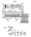
- Fig. 1 shows a printed circuit board Lp equipped with various components Bt, which is inserted into an outer frame Ra.
- Arrows Pf1 and Pf2 indicate that the frame Ra can be moved vertically upwards and downwards, this mobility of the frame Ra and the printed circuit board Lp being able to be achieved, for example, by a resilient suspension.
- a fixedly arranged lower needle adapter Nau which carries first spring-loaded contact needles Kn1 and somewhat shorter second spring-loaded contact needles Kn2.
- the contact needles Kn1 and Kn2 are connected via lines L to associated wrap spikes WS.
- the wrap spikes WS arranged outside the contacting area in the lower needle adapter Nau are in turn connected via an intermediate member Zg with resilient needles (not shown) to the needles of a connecting member Ag (also not shown).
- This connector Ag is part of the actual test machine, which can be, for example, the "Series 700" from Factron-Schlumberger, Albert Schweitzer Str. 66, D-8000 Kunststoff 83.
- lower pressure rams designated Asu
- Asu lower pressure rams
- the lower pressure rams Asu are therefore not designed to be resilient, but can be adjusted in two steps in the vertical direction via a common lower pressure plate Dp.
- This two-stage adjustability shown by double arrows Pf3 can be implemented, for example, by pneumatically or hydraulically actuated adjusting cylinders arranged under the pressure plate Dp.
- an upper needle adapter Nao which is adjustable in the vertical direction and which bears third spring-loaded contact needles Kn3 and somewhat shorter fourth spring-loaded contact needles Kn4.
- the further wiring of the contact needles Kn3 and Kn4, not shown, includes transfer contacts to the lower needle adapter Nau, so that the numerically mostly only a few upper test contacts are also connected to the automatic test machine via the interface of the intermediate member Zg.
- upper pressure rams labeled Aso are firmly arranged in the upper needle adapter Nao.
- These upper pressure plungers Aso are designed to be telescopically resilient, this resilient configuration being shown at one point by a corresponding spring F3.
- Two centering pins Zs which are also arranged in the upper needle adapter Nao, have the task of penetrating the centering holes in the printed circuit board Lp and thus positioning the printed circuit board Lp exactly.
- the vertical adjustability of the upper needle adapter Nao is shown by arrows Pf4, Pf5 and Pf6, the two downward arrows Pf5 and Pf6 having two stages symbolize the contact.
- the vertical adjustment can be realized, for example, in that the upper needle adapter Nao is guided in a solid four-column frame and, depending on the adapter size, is driven by one to four spindles synchronized by toothed belts via a DC motor.
- the drive of the pressure mechanism described is designed as a programmable positioning axis.
- FIG. 1 A preferred exemplary embodiment for the order of contacting the printed circuit board Lp in the test device shown in FIG. 1 is described below using the contacting scheme shown in FIG. 2.
- FIG. 2 On the left-hand side of FIG. 1, there is a highly simplified representation of a lower pressure ram Asu, lower first and second contact needles Kn1 and Kn2, part of the circuit board Lp to be contacted, an upper pressure ram Aso, a centering pin Zs and upper third and fourth Contact needles Kn3 or Kn4 shown.
- a position is shown in the initial stage of the contacting stroke of the upper needle adapter Nao, in which the centering pins Zs have penetrated into the associated centering holes Zb of the printed circuit board Lp and the spring-loaded upper pressure plungers Aso are already in contact with the printed circuit board Lp.
- the four successive contacting stages St1, St2, St3 and St4 are shown with the contact needles only indicated by arrows.
- the underside of the circuit board Lp is contacted by the first contact needles Kn1.
- the lower Asu plungers act here practically as a stop that limits the downward stroke of the circuit board Lp.
- the circuit board Lp is fixed clamped between the lower plungers Asu and the upper plungers Aso, ie the contacting state of the contacting stage St1 is clearly defined.
- the upper pressure rams Aso arranged in the upper needle adapter Nao have yielded so resiliently that there is now also reliable contacting of the upper side of the printed circuit board Lp by the third contact needles Kn3.
- the pressure plate Dp assumes its lower position, which is indicated by the downward direction of the arrows Pf3. Due to the correspondingly lower position of the lower pressure ram Asu and the printed circuit board Lp, reliable contacting of the underside of the board is now ensured by the second contact needles Kn2.
Landscapes
- Physics & Mathematics (AREA)
- General Physics & Mathematics (AREA)
- Tests Of Electronic Circuits (AREA)
- Testing Of Short-Circuits, Discontinuities, Leakage, Or Incorrect Line Connections (AREA)
Description
- Die Erfindung betrifft eine Prüfeinrichtung für bestückte Leiterplatten mittels beidseitiger, jeweils zweistufiger Kontaktierung.
- Für die elektrische Prüfung bestückter Leiterplatten, die auch als Flachbaugruppen bezeichnet werden können, sind Nadeladapter mit prüflingsspezifisch angeordneten Kontaktstiften im Einsatz. Man unterscheidet dabei zwischen Schaltkreistest oder Funktions- bzw. Teilfunktionstest. Bei der Prüfung wird die bestückte Leiterplatte mit der Lötseite gegen im Nadeladapter angeordnete, gefederte Kontaktnadeln gedrückt. Soll nun in derselben Prüfeinrichtung sowohl ein Schaltkreistest als auch ein Funktions- bzw. Teilfunktionstest durchgeführt werden, so ist eine zweistufige Kontaktierung mit unterschiedlich langen Kontaktnadeln vorzusehen. In der ersten Stufe der Kontaktierung kommen beim Funktions- bzw. Teilfunktionstest dann nur die langen Kontaktnadeln zum Eingriff, während in der zweiten Stufe der Kontaktierung beim Schaltkreistest die kurzen Kontaktnadeln hinzutreten.
- Die DE-C-35 11 821 zeigt und beschreibt eine Prüfeinrichtung für beidseitige, zweistufige Kontaktierung bestückter Leiterplatten, mit einem ersten Nadeladapter, der prüflingsspezifisch angeordnete und zur zweistufigen Kontaktierung der einen Seite der Leiterplatten unterschiedlich lange, erste und zweite gefederte Kontaktnadeln trägt, und mit einem zweiten Nadeladapter, der prüflingsspezifisch angeordnete und zur zweistufigen Kontaktierung der anderen Seite der Leiterplatten unterschiedlich lange, dritte und vierte gefederte Kontaktnadeln trägt. Zum Ausgleich der Druckkräfte bei ungleichmäßiger Verteilung der Kontaktnadeln auf den Nadeladaptern können Druckausgleichselemente auf den Nadeladaptern vorgesehen sein. Die Prüfung erfolgt in zwei Kontaktierstufen, wobei in der ersten Kontaktierstufe die Nadeladapter synchron aufeinander zu verschoben werden, bis jeweils die längeren Kontaktnadeln an der zu prüfenden Leiterplatte zur Anlage kommen. Danach werden die Nadeladapter noch weiter aufeinander zu verschoben, bis auch die kürzeren Kontaktnadeln in der zweiten Kontaktierstufe zur Anlage kommen.
- Im Zuge der sich immer mehr durchsetzenden SMD-Technologie wird die Forderung nach einer beidseitigen, jeweils zweistufigen Kontaktierung immer mehr erhoben werden.
- Das zur Kontaktierung erforderliche Andrücken der bestückten Leiterplatten kann über entsprechend verteilte Andruckstößel mechanisch vorgenommen werden. Häufiger im Einsatz sind jedoch sog. Vakuumadapter, bei denen die bestückte Leiterplatte manuell auf ein Dichtgummi gelegt und durch Erzeugung eines Vakuums angedrückt wird. Bei derartigen Vakuumadaptern stehen dem Vorteil einer besseren Zugänglichkeit an der Bauteileseite gleich mehrere Nachteile gegenüber. Da eine optimale Dosierung des Vakuums nicht möglich ist, können durch den hohen Flächendruck auftretende unzulässig hohe Durchbiegungen der Leiterplatten nicht sicher vermieden werden. Außerdem stellt die Abdichtung ein erhebliches Problem dar, so daß eine sichere Kontaktierung häufig nur durch Nachdrücken an bestimmten Stellen oder andere zusätzliche manuelle Eingriffe gewährleistet werden kann. Weiterhin ist das Spektrum der für die Prüfung im Vakuumadapter geeigneten Leiterplatten begrenzt, da beispielsweise keine offenen Durchkontaktierungen und Durchbrüche vorhanden sein sollen. Im Hinblick auf eine Automatisierung der Endprüfung bestückter Leiterplatten treten die vorstehend genannten Probleme noch stärker hervor. Insbesondere die Kontaktiersicherheit würde durch zusätzlich auftretende Dichtprobleme bei einem automatischen Wechsel der Leiterplatten weiter herabgesetzt.
- Der Erfindung liegt die Aufgabe zugrunde, eine Prüfeinrichtung für bestückte Leiterplatten mittels beidseitiger, jeweils zweistufiger Kontaktierung in vier aufeinanderfolgenden Kontaktierstufen zu schaffen, die bei automatisierungsfreundlichem Aufbau und ohne die Gefahr unzulässig hoher Durchbiegungen der Leiterplatten eine hohe Kontaktiersicherheit gewährleistet. Außerdem soll die Prüfeinrichtung den Anforderungen der SMD-Technologie gerecht werden.
- Diese Aufgabe wird durch die Merkmale des Anspruchs 1 gelöst.
- Die erfindungsgemäße Prüfeinrichtung ermöglicht somit eine beidseitig, jeweils zweistufige Kontaktierung bestückter Leiterplatten in vier aufeinanderfolgenden Kontaktierstufen, die insbesondere durch die mechanische Einspannung der Leiterplatten zwischen oberen und unteren Andruckstößeln realisiert wird. Die Fixierung der Leiterplatte ist unabhängig von Anzahl und Verteilung der Kontaktnadeln in jeder Kontaktierstufe gegeben, wodurch der Kontaktierzustand zu jedem Zeitpunkt eindeutig definiert ist. Die Andruckstößel sind dabei Bestandteil der prüflingsspezifisch austauschbaren Nadeladapter der Prüfeinrichtung.
- Gemäß einer bevorzugten Ausgestaltung der Erfindung ist der untere Nadeladapter ortsfest angeordnet. Da der untere Nadeladapter somit auch beim Kontaktiervorgang nicht bewegt wird, kann die elektrische Prüfsicherheit hier auch nicht durch eine bewegte Verdrahtung beeinträchtigt werden.
- Eine weitere vorteilhafte Ausgestaltung der Erfindung sieht vor, daß die Leiterplatten mit federnd ausgebildeten oberen Andruckstößeln gegen den ortsfest angeordneten unteren Nadeladapter drückbar sind, wobei die Kräfte der federnden oberen Andruckstößel in der Summe größer sind als die Summe der Federkräfte der dritten und vierten Kontaktnadeln. Durch diese Maßnahme ist zu jedem Zeitpunkt das Kräfteverhältnis gewahrt und der Kontaktierzustand eindeutig definiert.
- Der obere Nadeladapter ist vorzugsweise in vertikaler Richtung verstellbar angeordnet. In diesem Fall können dann die federnden oberen Andruckstößel fest im oberen Nadeladapter angeordnet werden. Der obere Nadeladapter und die oberen Andruckstößel können somit über einen gemeinsamen Antrieb bewegt werden.
- Gemäß einer weiteren Ausgestaltung der Erfindung ist vorgesehen, daß die unteren Andruckstößel in vertikaler Richtung in zwei Stufen verstellbar sind. Durch diese zweistufige Verstellbarkeit wird die zweistufige Kontaktierung der Plattenunterseite auf besonders einfache Weise realisiert. Dabei sind die unteren Andruckstößel vorzugsweise im unteren Nadeladapter geführt und über eine untere gemeinsame Druckplatte betätigbar. Bei einem prüflingsspezifischen Austausch des unteren Nadeladapters mit den unteren Andruckstößeln können dann die Druckplatte und deren Antrieb stets in der Prüfeinrichtung verbleiben.
- Eine genaue und besonders einfache Positionierung der Leiterplatten wird schließlich dadurch erreicht, daß im oberen Nadeladapter mindestens zwei den oberen Andruckstößeln vorauseilende Zentrierstifte angeordnet sind.
- Ein Ausführungsbeispiel der Erfindung ist in der Zeichnung dargestellt und wird im folgenden näher beschrieben.
- Es zeigen
- Fig. 1
- eine Prüfeinrichtung für beidseitige zweistufige Kontaktierung bestückter Leiterplatten in stark vereinfachter schematischer Darstellung und
- Fig. 2
- die einzelnen Stufen der Kontaktierung der Prüfeinrichtung gemäß Fig. 1.
- Fig. 1 zeigt eine mit verschiedenen Bauteilen Bt bestückte Leiterplatte Lp, die in einen äußeren Rahmen Ra eingelegt ist. Pfeile Pf1 und Pf2 zeigen an, daß der Rahmen Ra in vertikaler Richtung nach oben und unten beweglich ist, wobei diese Beweglichkeit von Rahmen Ra und Leiterplatte Lp beispielsweise durch eine federnde Aufhängung realisiert werden kann.
- Unterhalb der Leiterplatte Lp befindet sich ein ortsfest angeordneter unterer Nadeladapter Nau, der erste gefederte Kontaktnadeln Kn1 und etwas kürzere zweite gefederte Kontaktnadeln Kn2 trägt. An einer Stelle ist angedeutet, daß die Kontaktnadeln Kn1 und Kn2 über Leitungen L mit zugeordneten Wrap-Stacheln WS verbunden sind. Die außerhalb des Kontaktierungsbereichs im unteren Nadeladapter Nau angeordneten Wrap-Stacheln WS sind ihrerseits über ein Zwischenglied Zg mit nicht näher bezeichneten federnden Nadeln mit den ebenfalls nicht näher bezeichneten Nadeln eines Anschlußgliedes Ag verbunden. Dieses Anschlußglied Ag ist Teil des eigentlichen Prüfautomaten, bei welchem es sich beispielsweise um die "Series 700" der Firma Factron-Schlumberger, Albert Schweitzer Str. 66, D-8000 München 83 handeln kann.
- Im unteren Nadeladapter Nau sind ferner mit Asu bezeichnete untere Andruckstößel geführt, die über Federn F1 in vertikaler Richtung beweglich im Nadeladapter Nau gehalten sind. Die unteren Andruckstößel Asu sind also nicht federnd ausgebildet, sondern über eine gemeinsame untere Druckplatte Dp in vertikaler Richtung in zwei Stufen verstellbar. Diese durch Doppelpfeile Pf3 aufgezeigte zweistufige Verstellbarkeit kann beispielsweise durch unter der Druckplatte Dp angeordnete pneumatisch oder hydraulisch betätigbare Verstellzylinder realisiert werden.
- Über der Leiterplatte Lp befindet sich ein in vertikaler Richtung verstellbar angeordneter oberer Nadeladapter Nao, der dritte gefederte Kontaktnadeln Kn3 und etwas kürzere vierte gefederte Kontaktnadeln Kn4 trägt. Die nicht näher dargestellte Weiterverdrahtung der Kontaktnadeln Kn3 und Kn4 umfaßt Übergabekontakte zum unteren Nadeladapter Nau, so daß die zahlenmäßig meist nur wenigen oberen Prüfkontakte ebenfalls über die Schnittstelle des Zwischengliedes Zg an den Prüfautomaten angeschlossen sind.
- Im oberen Nadeladapter Nao sind mit Aso bezeichnete obere Andruckstößel fest angeordnet. Diese oberen Andruckstößel Aso sind teleskopartig federnd ausgebildet, wobei diese federnde Ausgestaltung an einer Stelle durch eine entsprechende Feder F3 aufgezeigt ist. Zwei ebenfalls im oberen Nadeladapter Nao angeordnete Zentrierstifte Zs haben die Aufgabe in zugeordnete Zentrierbohrungen der Leiterplatte Lp einzudringen und damit die Leiterplatte Lp genau zu positionieren.
- Die vertikale Verstellbarkeit des oberen Nadeladapters Nao ist durch Pfeile Pf4, Pf5 und Pf6 aufgezeigt, wobei die beiden nach unten gerichteten Pfeile Pf5 und Pf6 die Zweistufigkeit der Kontaktierung symbolisieren sollen. Die vertikale Verstellung kann beispielsweise dadurch realisiert werden, daß der obere Nadeladapter Nao in einem massiven Vier-Säulengestell geführt und je nach Adaptergröße durch ein bis vier mittels Zahnriemen synchronisierte Spindeln über einen Gleichstrommotor angetrieben wird. Der geschilderte Antrieb der Andruckmechanik ist dabei als programmierbare Positionierachse ausgeführt.
- Nachfolgend wird unter Hinzuziehung des in Fig. 2 dargestellten Kontaktierschemas ein bevorzugtes Ausführungsbeispiel für die Reihenfolge der Kontaktierung der Leiterplatte Lp in der in Fig. 1 dargestellten Prüfeinrichtung beschrieben. Auf der linken Seite der Fig. 1 sind dabei in stark vereinfachter Darstellung ein unterer Andruckstößel Asu, untere erste und zweite Kontaktnadeln Kn1 bzw. Kn2, ein Teil der zu kontaktierenden Leiterplatte Lp, ein oberer Andruckstößel Aso, ein Zentrierstift Zs und obere dritte und vierte Kontaktnadeln Kn3 bzw. Kn4 aufgezeigt. Es ist dabei eine Stellung im Anfangsstadium des Kontaktierhubes des oberen Nadeladapters Nao dargestellt, in welcher die Zentrierstifte Zs in die zugeordneten Zentrierbohrungen Zb der Leiterplatte Lp eingedrungen sind und auch die gefederten oberen Andruckstößel Aso bereits an der Leiterplatte Lp anliegen. Rechts von dieser Darstellung sind mit dem nur noch durch Pfeile angedeuteten Kontaktnadeln die vier aufeinanderfolgenden Kontaktierstufen St1, St2, St3 und St4 aufgezeigt.
- In der ersten Kontaktierstufe St1 erfolgt die Kontaktierung der Unterseite der Leiterplatte Lp durch die ersten Kontaktnadeln Kn1. Die unteren Andruckstößel Asu wirken hier praktisch als Anschlag, der den Abwärtshub der Leiterplatte Lp begrenzt. Die Leiterplatte Lp ist dabei fest zwischen den unteren Andruckstößeln Asu und den oberen Andruckstößeln Aso eingespannt, d.h. der Kontaktierzustand der Kontaktierstufe St1 ist eindeutig definiert.
- In der zweiten Kontaktierstufe St2 haben die im oberen Nadeladapter Nao angeordneten oberen Andruckstößel Aso so weit federnd nachgegeben, daß nun auch eine sichere Kontaktierung der Oberseite der Leiterplatte Lp durch die dritten Kontaktnadeln Kn3 vorliegt.
- In der dritten Kontaktierstufe St3 nimmt die Druckplatte Dp ihre durch die Abwärtsrichtung der Pfeile Pf3 angedeutete untere Lage ein. Durch die entsprechend tiefere Lage der unteren Andruckstößel Asu und der Leiterplatte Lp ist nunmehr eine sichere Kontaktierung der Plattenunterseite durch die zweiten Kontaktnadeln Kn2 gewährleistet.
- In der vierten Kontaktierstufe St4 ist schließlich durch eine weitere Abwärtsbewegung des oberen Nadeladapters Nao bei gleichzeitigem weiteren federnden Nachgeben der oberen Andruckstößel Aso eine Kontaktierung der Plattenoberseite durch die vierten Kontaktnadeln Kn4 eingetreten.
- Es ist zu erkennen, daß nicht nur in der ersten Kontaktierstufe St1, sondern auch in den folgenden Kontaktierstufen St2, St3 und St4 durch eine feste Einspannung der Leiterplatte Lp zwischen den unteren und oberen Andruckstößeln Asu bzw. Aso jeweils eindeutig definierte Kontaktierzustände gewährleistet sind. Es ist ferner zu erkennen, daß für die Reihenfolge der Kontaktierungen etliche Variationen möglich sind.
Claims (8)
- Prüfeinrichtung für bestückte Leiterplatten (Lp) mittels beidseitiger, jeweils zweistufiger Kontaktierung in vier aufeinanderfolgenden Kontaktierstufen (St 1, St 2, St 3, St 4), mit- einem unteren Nadeladapter (Nau), der prüflingsspezifisch angeordnete und zur zweistufigen Kontaktierung der Unterseiten der Leiterplatten (Lp) unterschiedlich lange, erste und zweite gefederte Kontaktnadeln (Ku 1, Ku 2) trägt,- einem oberen Nadeladapter (Nao), der prüflingsspezifisch angeordnete und zur zweistufigen Kontaktierung der Oberseiten der Leiterplatten (Lp) unterschiedlich lange dritte und vierte gefederte Kontaktnadeln (Ku 3, Ku 4) trägt,- mehreren prüflingsspezifisch angeordneten unteren Andruckstößeln (Asu) und mit- mehreren prüflingsspezifisch angeordneten oberen Andruckstößeln (Aso), wobei- die Leiterplatten (Lp) zwischen den unteren Andruckstößeln (Asu) und den oberen Andruckstößeln (Aso) eingespannt sind.
- Prüfeinrichtung nach Anspruch 1, dadurch gekennzeichnet, daß der untere Nadeladapter (Nau) ortsfest angeordnet ist.
- Prüfeinrichtung nach Anspruch 2, dadurch gekennzeichnet, daß die Leiterplatten (Lp) mit federnd ausgebildeten oberen Andruckstößeln (Aso) gegen den ortsfest angeordneten unteren Nadeladapter (Nau) drückbar sind, wobei die Kräfte der federnden oberen Andruckstößel (Aso) in der Summe größer sind als die Summe der Federkräfte der dritten und vierten Kontaktnadeln (Kn3, Kn4).
- Prüfeinrichtung nach einem der vorhergehenden Ansprüche, dadurch gekennzeichnet, daß der obere Nadeladapter (Nao) in vertikaler Richtung verstellbar angeordnet ist.
- Prüfeinrichtung nach den Ansprüchen 3 und 4, dadurch gekennzeichnet, daß die federnden oberen Andruckstößel (Aso) fest im oberen Nadeladapter (Nao) angeordnet sind.
- Prüfeinrichtung nach einem der vorhergehenden Ansprüche, dadurch gekennzeichnet, daß die unteren Andruckstößel (Asu) in vertikaler Richtung in zwei Stufen verstellbar sind.
- Prüfeinrichtung nach Anspruch 6, dadurch gekennzeichnet, daß die unteren Andruckstößel (Asu) im unteren Nadeladapter (Nau) geführt und über eine untere gemeinsame Druckplatte (Dp) betätigbar sind.
- Prüfeinrichtung nach einem der vorhergehenden Ansprüche, dadurch gekennzeichnet, daß zur Positionierung der Leiterplatten (Lp) im oberen Nadeladapter (Nao) mindestens zwei den oberen Andruckstößeln (Aso) vorauseilende Zentrierstifte (Zs) angeordnet sind.
Applications Claiming Priority (2)
| Application Number | Priority Date | Filing Date | Title |
|---|---|---|---|
| DE3626758 | 1986-08-07 | ||
| DE3626758 | 1986-08-07 |
Publications (2)
| Publication Number | Publication Date |
|---|---|
| EP0256368A1 EP0256368A1 (de) | 1988-02-24 |
| EP0256368B1 true EP0256368B1 (de) | 1992-09-30 |
Family
ID=6306878
Family Applications (1)
| Application Number | Title | Priority Date | Filing Date |
|---|---|---|---|
| EP87110884A Expired - Lifetime EP0256368B1 (de) | 1986-08-07 | 1987-07-27 | Prüfeinrichtung für beidseitige, zweistufige Kontaktierung bestückter Leiterplatten |
Country Status (3)
| Country | Link |
|---|---|
| US (1) | US5068600A (de) |
| EP (1) | EP0256368B1 (de) |
| DE (1) | DE3781979D1 (de) |
Families Citing this family (14)
| Publication number | Priority date | Publication date | Assignee | Title |
|---|---|---|---|---|
| DE68917231T2 (de) * | 1988-05-18 | 1994-12-15 | Canon Kk | Sondenkarte, Verfahren zur Messung eines zu messenden Teiles mit derselben und elektrischer Schaltungsteil. |
| US4912400A (en) * | 1988-09-13 | 1990-03-27 | Design And Manufacturing Specialties, Inc. | Apparatus for testing circuit boards |
| US5572144A (en) * | 1993-02-22 | 1996-11-05 | Seagate Technology | Test jig and method for probing a printed circuit board |
| US5473254A (en) * | 1994-08-12 | 1995-12-05 | At&T Corp. | Test probe assembly provides precise and repeatable contact forces |
| IT1282827B1 (it) * | 1995-09-22 | 1998-03-31 | New System Srl | Macchina per il controllo contrapposto dei circuiti stampati |
| NZ315085A (en) * | 1995-12-22 | 2007-12-21 | New System Srl | Testing printed circuit boards, two coplanar boards containing test needles movable with respect to each other |
| US5764071A (en) * | 1996-01-05 | 1998-06-09 | International Business Machines Corporation | Method and system for testing an electronic module mounted on a printed circuit board |
| US5698990A (en) * | 1996-07-10 | 1997-12-16 | Southwest Test Inc. | Counterforce spring assembly for printed circuit board test fixtures |
| US6614221B2 (en) * | 2002-01-07 | 2003-09-02 | Tektronix, Inc. | Deskew fixture |
| US7385408B1 (en) | 2005-07-12 | 2008-06-10 | Amkor Technology, Inc. | Apparatus and method for testing integrated circuit devices having contacts on multiple surfaces |
| CN102288792B (zh) * | 2011-07-22 | 2013-10-02 | 华为终端有限公司 | 测试夹具 |
| FR2983969B1 (fr) * | 2011-12-07 | 2014-12-05 | Larisys Ind | Dispositif de controle de cartes electroniques. |
| JP6721302B2 (ja) * | 2015-08-10 | 2020-07-15 | 東京特殊電線株式会社 | 両面回路基板の検査装置 |
| TWI766424B (zh) * | 2020-11-05 | 2022-06-01 | 南茂科技股份有限公司 | 氣動夾具與應用於氣動夾具的導電軟板 |
Family Cites Families (10)
| Publication number | Priority date | Publication date | Assignee | Title |
|---|---|---|---|---|
| US4115735A (en) * | 1976-10-14 | 1978-09-19 | Faultfinders, Inc. | Test fixture employing plural platens for advancing some or all of the probes of the test fixture |
| GB1530350A (en) * | 1976-10-23 | 1978-10-25 | Marconi Instruments Ltd | Electrical test jigs |
| US4335350A (en) * | 1980-05-23 | 1982-06-15 | Chen James T C | Apparatus for probing semiconductor wafers |
| GB2108774B (en) * | 1981-10-21 | 1985-01-09 | Marconi Instruments Ltd | Electrical interface arrangements |
| US4625164A (en) * | 1984-03-05 | 1986-11-25 | Pylon Company | Vacuum actuated bi-level test fixture |
| GB2172150B (en) * | 1985-03-05 | 1988-06-08 | Marconi Instruments Ltd | Probe arrays for testing circuit boards |
| US4626779A (en) * | 1985-03-19 | 1986-12-02 | Pylon Company, Inc. | Spring-stops for a bi-level test fixture |
| DE3511821C1 (de) * | 1985-03-30 | 1986-06-19 | Rohde & Schwarz GmbH & Co KG, 8000 München | Adapter zur Aufnahme von beidseitig zu prüfenden Leiterplatten |
| US4841241A (en) * | 1986-08-07 | 1989-06-20 | Siemens Aktiengesellschaft | Testing device for both-sided contacting of component-equipped printed circuit boards |
| US4818933A (en) * | 1986-10-08 | 1989-04-04 | Hewlett-Packard Company | Board fixturing system |
-
1987
- 1987-07-27 EP EP87110884A patent/EP0256368B1/de not_active Expired - Lifetime
- 1987-07-27 DE DE8787110884T patent/DE3781979D1/de not_active Expired - Lifetime
-
1990
- 1990-05-23 US US07/528,340 patent/US5068600A/en not_active Expired - Fee Related
Also Published As
| Publication number | Publication date |
|---|---|
| EP0256368A1 (de) | 1988-02-24 |
| US5068600A (en) | 1991-11-26 |
| DE3781979D1 (de) | 1992-11-05 |
Similar Documents
| Publication | Publication Date | Title |
|---|---|---|
| EP0255909B1 (de) | Prüfeinrichtung für beidseitige Kontaktierung bestückter Leiterplatten | |
| EP0256368B1 (de) | Prüfeinrichtung für beidseitige, zweistufige Kontaktierung bestückter Leiterplatten | |
| DE2659977C2 (de) | Vorrichtung zur Herstellung einer elektrischen Verbindung zwischen einem in einer statischen elektrischen Prüfung befindlichen Bauteil und einer Prüfeinrichtung | |
| EP0026824B2 (de) | Adapter für eine Vorrichtung zur elektronischen Prüfung von Leiterplatten | |
| DE3812654C2 (de) | ||
| DE3785977T2 (de) | Maschine zur positionierung von chips mit prueffunktion. | |
| DE2707900C3 (de) | Universal-Adaptiervorrichtung für Geräte zur elektrischen Prüfung unterschiedlicher gedruckter Schaltungen | |
| DE2163970A1 (de) | Prutgerat fur Tafeln mit gedruckter Schaltung | |
| EP0224471B1 (de) | Vorrichtung zum Prüfen von Leiterplatten | |
| DE69203260T2 (de) | Andrückvorrichtung und Verfahren. | |
| EP0315707A1 (de) | Adapter für eine Vorrichtung zur elektronischen Prüfung von Leiterplatten | |
| DE69508127T2 (de) | Markierungssystem für Leiterplatten | |
| DE3136896A1 (de) | Vorrichtung zum pruefen einer elektronischen leiterplatte | |
| DE2905175A1 (de) | Adaptiervorrichtung fuer das verbinden von zu pruefenden elektronikbaugruppen mit pruefgeraeten | |
| DE3148285C2 (de) | Prüfadapter zum Anschließen von zu prüfenden Elektronik-Flachbaugruppen an ein Universal-Prüfgerät | |
| EP0513570B1 (de) | Einrichtung zum Prüfen des Vorhandenseins von Setzstiften in einer Leiterplatte beim automatischen Einsetzen der Setzstifte | |
| DE8621220U1 (de) | Prüfeinrichtung für beidseitige, zweistufige Kontaktierung bestückter Leiterplatten | |
| DE3405567A1 (de) | Einrichtung zur lagegenauen positionierung von flachbaugruppen auf pruefadaptern (pendelnde fuehrungsnadeln) | |
| DE3248796C2 (de) | Pneumatische Kontaktiereinrichtung zur automatischen Prüfung von Flachbaugruppen | |
| DE19610328A1 (de) | Zuleitungsanpreßvorrichtung für ein IC-Test-Handhabungsgerät | |
| DE8621171U1 (de) | Prüfeinrichtung für beidseitige Kontaktierung bestückter Leiterplatten | |
| DE19514163A1 (de) | Verfahren und Vorrichtung zum vollautomatischen Handhaben von elektrisch zu prüfenden Prüflingen | |
| EP0146782B1 (de) | Adaptereinrichtung zur Herstellung einer lösbaren elektrischen Verbindung zwischen Kontaktelementen eines ersten elektrischen Bauteils und Kontaktelementen eines zweiten elektrischen Bauteils | |
| DE3212456C2 (de) | Vorrichtung zur Herstellung einer Steckverbindung zwischen den Kontaktelementen einer Flachbaugruppe und den Kontaktelementen eines Adapters | |
| DE4436354A1 (de) | Vorrichtung zum gleichzeitigen Prüfen einer Mehrzahl von elektrischen oder elektronischen Teilen |
Legal Events
| Date | Code | Title | Description |
|---|---|---|---|
| PUAI | Public reference made under article 153(3) epc to a published international application that has entered the european phase |
Free format text: ORIGINAL CODE: 0009012 |
|
| AK | Designated contracting states |
Kind code of ref document: A1 Designated state(s): BE DE FR GB IT SE |
|
| 17P | Request for examination filed |
Effective date: 19880425 |
|
| 17Q | First examination report despatched |
Effective date: 19901126 |
|
| GRAA | (expected) grant |
Free format text: ORIGINAL CODE: 0009210 |
|
| AK | Designated contracting states |
Kind code of ref document: B1 Designated state(s): BE DE FR GB IT SE |
|
| REF | Corresponds to: |
Ref document number: 3781979 Country of ref document: DE Date of ref document: 19921105 |
|
| ET | Fr: translation filed | ||
| ITF | It: translation for a ep patent filed | ||
| GBT | Gb: translation of ep patent filed (gb section 77(6)(a)/1977) |
Effective date: 19921209 |
|
| PGFP | Annual fee paid to national office [announced via postgrant information from national office to epo] |
Ref country code: GB Payment date: 19930618 Year of fee payment: 7 |
|
| PGFP | Annual fee paid to national office [announced via postgrant information from national office to epo] |
Ref country code: FR Payment date: 19930716 Year of fee payment: 7 |
|
| PGFP | Annual fee paid to national office [announced via postgrant information from national office to epo] |
Ref country code: BE Payment date: 19930723 Year of fee payment: 7 |
|
| PGFP | Annual fee paid to national office [announced via postgrant information from national office to epo] |
Ref country code: SE Payment date: 19930727 Year of fee payment: 7 |
|
| PLBE | No opposition filed within time limit |
Free format text: ORIGINAL CODE: 0009261 |
|
| STAA | Information on the status of an ep patent application or granted ep patent |
Free format text: STATUS: NO OPPOSITION FILED WITHIN TIME LIMIT |
|
| PGFP | Annual fee paid to national office [announced via postgrant information from national office to epo] |
Ref country code: DE Payment date: 19930915 Year of fee payment: 7 |
|
| 26N | No opposition filed | ||
| PG25 | Lapsed in a contracting state [announced via postgrant information from national office to epo] |
Ref country code: GB Effective date: 19940727 |
|
| PG25 | Lapsed in a contracting state [announced via postgrant information from national office to epo] |
Ref country code: SE Effective date: 19940728 |
|
| PG25 | Lapsed in a contracting state [announced via postgrant information from national office to epo] |
Ref country code: BE Effective date: 19940731 |
|
| BERE | Be: lapsed |
Owner name: SIEMENS A.G. Effective date: 19940731 |
|
| EUG | Se: european patent has lapsed |
Ref document number: 87110884.1 Effective date: 19950210 |
|
| GBPC | Gb: european patent ceased through non-payment of renewal fee |
Effective date: 19940727 |
|
| PG25 | Lapsed in a contracting state [announced via postgrant information from national office to epo] |
Ref country code: FR Effective date: 19950331 |
|
| PG25 | Lapsed in a contracting state [announced via postgrant information from national office to epo] |
Ref country code: DE Effective date: 19950401 |
|
| EUG | Se: european patent has lapsed |
Ref document number: 87110884.1 |
|
| REG | Reference to a national code |
Ref country code: FR Ref legal event code: ST |
|
| PG25 | Lapsed in a contracting state [announced via postgrant information from national office to epo] |
Ref country code: IT Free format text: LAPSE BECAUSE OF NON-PAYMENT OF DUE FEES;WARNING: LAPSES OF ITALIAN PATENTS WITH EFFECTIVE DATE BEFORE 2007 MAY HAVE OCCURRED AT ANY TIME BEFORE 2007. THE CORRECT EFFECTIVE DATE MAY BE DIFFERENT FROM THE ONE RECORDED. Effective date: 20050727 |