EP0256498A2 - Compensateur d'écriture pour un appareil à disque magnétique - Google Patents
Compensateur d'écriture pour un appareil à disque magnétique Download PDFInfo
- Publication number
- EP0256498A2 EP0256498A2 EP87111631A EP87111631A EP0256498A2 EP 0256498 A2 EP0256498 A2 EP 0256498A2 EP 87111631 A EP87111631 A EP 87111631A EP 87111631 A EP87111631 A EP 87111631A EP 0256498 A2 EP0256498 A2 EP 0256498A2
- Authority
- EP
- European Patent Office
- Prior art keywords
- write
- recording data
- compensation information
- data
- write compensation
- Prior art date
- Legal status (The legal status is an assumption and is not a legal conclusion. Google has not performed a legal analysis and makes no representation as to the accuracy of the status listed.)
- Granted
Links
- 230000003111 delayed effect Effects 0.000 claims description 11
- 238000006243 chemical reaction Methods 0.000 abstract description 5
- 238000010586 diagram Methods 0.000 description 3
- 230000006870 function Effects 0.000 description 3
- 230000001934 delay Effects 0.000 description 2
- 230000000717 retained effect Effects 0.000 description 2
- 230000007423 decrease Effects 0.000 description 1
- 230000003247 decreasing effect Effects 0.000 description 1
- 230000002035 prolonged effect Effects 0.000 description 1
Images




Classifications
-
- G—PHYSICS
- G11—INFORMATION STORAGE
- G11B—INFORMATION STORAGE BASED ON RELATIVE MOVEMENT BETWEEN RECORD CARRIER AND TRANSDUCER
- G11B20/00—Signal processing not specific to the method of recording or reproducing; Circuits therefor
- G11B20/10—Digital recording or reproducing
-
- G—PHYSICS
- G11—INFORMATION STORAGE
- G11B—INFORMATION STORAGE BASED ON RELATIVE MOVEMENT BETWEEN RECORD CARRIER AND TRANSDUCER
- G11B20/00—Signal processing not specific to the method of recording or reproducing; Circuits therefor
- G11B20/10—Digital recording or reproducing
- G11B20/10009—Improvement or modification of read or write signals
- G11B20/10046—Improvement or modification of read or write signals filtering or equalising, e.g. setting the tap weights of an FIR filter
- G11B20/10212—Improvement or modification of read or write signals filtering or equalising, e.g. setting the tap weights of an FIR filter compensation for data shift, e.g. pulse-crowding effects
Definitions
- the present invention relates to a write compensator for a magnetic recording/reproducing apparatus for performing high-density recording.
- a peak shift occurs in a data pulse due to the influence of adjacent bits when data is read out from a disk. This decreases time margins for data and clock windows. When the margins are excessively decreased, an error rate is reduced.
- Figs. lA through lE show a case wherein recording data externally transferred in the nonreturn-to-zero (NRZ) format for high-density recording is converted into recording data in the modified frequency modulation (MFM) format, and the converted data is written in a recording medium.
- Fig. lA shows a data transfer reference clock
- Fig. lB shows NRZ recording data.
- the NRZ recording data shown in Fig. lB is transferred in synchronism with the reference clock shown in Fig. lA.
- the NRZ recording data is converted into MFM recording data shown in Fig. lE in accordance with MFM conversion rules in the magnetic disk apparatus in response to clock and data pulses shown in Figs. lC and lD.
- the converted data is written in the magnetic recording medium. In this case, peak shifts occur in the data patterns shown in Figs. 2A through 2D.
- phase shift directions are changed in accordance with different data pulse trains, as indicated by arrows.
- clock pulse C2 repulses clock and data pulses Cl and Dl.
- clock pulse C2 is closer to clock pulse Cl than to data pulse Dl. Therefore, clock pulse C2 repulses clock pulse Cl and is shifted in a direction of an arrow.
- data pulse D2 is closer to data pulse D3 than to clock pulse C3. Therefore, data pulse D2 repulses data pulse D3 and is shifted in a direction of an arrow.
- Peak shifts can be predicted in the data write mode in accordance with data pulse patterns.
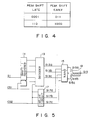
- Data patterns subjected to peak shifts are summarized as follows. When data pulse patterns are "000l” and “ll0” shown in Fig. 4, late peak shifts occur. However, if data pulse patterns are “0ll” and “l000”, early peak shifts occur, as shown in Fig. 4. Therefore, when recording data have patterns "0ll” and "l000”, respectively, the data are shifted in directions of arrows (right direction) in Figs. 2A and 2B, i.e., in directions opposite to the read direction. However, when recording data have patterns "ll0" and "000l”, repectively, data are shifted in directions of arrows (left direction) in Figs. 2C and 2D, thereby achieving write compensation.
- Shift register ll stores externally transferred NRZ recording data Sl in synchronism with reference clock signal CSl and outputs it to decoder l3.
- Decoder l3 has a function for converting NRZ recording data Sl into MFM recording data S2 and a function for producing write compensation information by decoding a pattern of data S2. More specifically, NRZ recording data Sl is converted into MFM recording data S2 in response to reference clock signals CSl and CS2. The pattern of data S2 is decoded to generate signal Sl3a for compensation in an "early: direction (i.e., a direction in which a write timing advances), non-compensation signal l3b, or signal l3c for compensation in a "late" direction (i.e., a direction in which a write timing is delayed). Signal l3a, l3b, or l3c is output to NAND gate l5.
- Delay circuit l7 delays reference clock signal CS2 by delay times D0, Dl, and D2 to obtain signals Sl7a, Sl7b, and Sl7c. Signals Sl7a, Sl7b, and Sl7c are input to NAND gate l5.
- Signals Sl3a, Sl3b, and Sl3c from decoder l3 are logically NANDed by NAND gate l5 with signals Sl7a, Sl7b, and Sl7c from delay circuit l7.
- Output signals Sl5a, Sl5b, and Sl5c from NAND gate l5 are input to NAND gate l9.
- Signals Sl5a, Sl5b, and Sl5c are logically NANDed by NAND gate l9, and NAND gate l9 outputs write-compensated MFM recording data Sl9.
- Decoder l3 decodes recording data Sl (Fig. 6C) from register ll in response to reference clock signals CSl and CS2 and generates MFM recording data S2 (Fig. 6D).
- Two reference clock signals CSl and CS2 are used to assure accurate synchronization timings.
- a sync signal required in write compensation is only signal CSl, and signal CSl must be a signal having an accurate waveform.
- signal CS2 having a frequency twice that of signal CSl is produced and is frequency-divided to generate signal CSl having an accurate waveform.
- Decoder l3 decodes the pattern of converted recording data S2 to determine necessity of write compensation and generates write compensation information as needed.
- Compensation information signal Sl3a (Fig. 6E) for compensating recording data S2 in the early direction
- noncompensation information signal Sl3b and compensation information signal Sl3c (Fig. 6F) for compensating data S2 in the late direction are output from decoder l3 to NAND gate l5. Since the pattern of recording data Sl is "000l", as shown in Fig. 6C, pulse 35 in recording data S2 is delayed, as shown in Fig. 6D.
- Signal Sl3a for compensating the write timing in the early direction is output between trailing edges 3la and 3lb of reference clock signal CSl. As shown in Fig.
- pulse 37 in recording data S2 is advanced, as shown in Fig. 6D. Therefore, signal Sl3c for compensating the write timing in the late direction is output between trailing edges 33a and 33b of reference clock signal CSl. Noncompensation information signal S3b (not shown) is output for pulses not subjected to compensation between the current and next trailing edges of reference clock signal CSl.
- delayed signals Sl7a, Sl7b, and Sl7c obtained by delaying reference clock signal CS2 by delay times D0, Dl, and D2 are output from delay circuit l7 to NAND gate l5.
- Signals Sl3a, Sl3b, and Sl3c from decoder l3 and signals Sl7a, Sl7b, and Sl7c from delay circuit l7 are logically NANDed by NAND gate l5, and output signals Sl5a, Sl5b, and Sl5c therefrom are output to NAND gate l9.
- Signals Sl5a, Sl5b, and Sl5c from NAND gate l5 are logically NANDed by NAND gate l9.
- Write-compensated MFM recording data Sl9 is output from NAND gate l9.
- Fig. 6G shows write-compensated MFM recording data. No shift occurs in MFM recording data 4l in Fig. 6D.
- Delay time Dl is assigned to pulse 4l as indicated by pulse 43 in Fig. 6G.
- delay time D0 shorter than delay time Dl is given to pulse 35 to compensate for the time (Dl - D0) in the early direction (direction indicated by arrow 5l), as indicated by pulse 45 in Fig. 6G.
- Pulse 37 is shifted in the early direction, as shown in Fig. 6D. Therefore, delay time D2 longer than delay time Dl is given to pulse 37 to compensate for (D2 - Dl) in the late direction (direction indicated by arrow 53), as indicated by pulse 47 in Fig. 6G.
- the above write compensator is used to automatically shift write timings in a direction to reduce peak shifts.
- the delay time length of the write compensation information signal is determined by the duration of the reference clock signal.
- Time length J of signal Sl3a for compensating write timings in the early direction and time length K of signal Sl3c for compensating the write timings in the late direction must fall within the length of time between the current and next trailing edges of reference clock signal CSl due to the following reason.
- Recording data Sl is shifted and shift register ll outputs different values to decoder l3 whenever reference signal CSl is input to shift register ll. Decoder l3 must completely decode the input before the output signal from register ll is updated.
- each delay time length of signals Sl3a, Sl3b, and Sl3c cannot exceed one cycle of reference signal CSl. Therefore, ranges of delay times D0, Dl, and D2 (i.e., delay times D0, Dl, and D2 of signals Sl7a, Sl7b, and Sl7c) of write-compensated recording data S6 are solely determined.
- data converting means for converting input recording data into a predetermined recording data format
- write compensation information generating means for generating write compensation information on the basis of a conversion pattern of the input recording data or a data pattern of the recording data converted by said data converting means
- write compensation information storing means for storing the write compensation information from said write compensation information generating means on the basis of the recording data converted by said data converting means
- write-compensating means for performing write compensation of the converted recording data on the basis of the write compensation information stored in said write compensation information storing means.
- Fig. 7 is a block diagram of a write compensator for a magnetic disk apparatus according to an embodiment of the present invention.
- decoder 2l decodes NRZ recording data Sl stored in shift register ll.
- the decoded output serves as MFM recording data S2.
- Decoder 2l decodes the data pattern of data S2 to determine necessity of compensation and generates write compensation information signals S2la, S2lb, and S2lc as needed.
- write compensation information signal S2la for compensating recording data S2 in the early direction write compensation information signal S2lb for noncompensation
- write compensation information signal S2lc for compensating recording data S2 in the late direction are output to flip-flop 23.
- Decoder 2l has a function for supplying signal S22 representing generation of MFM recording data S2 to AND gate 25.
- Signal S22 (Fig. 8D) output from decoder 23 is a signal representing that recording data S2 shown in Fig. 8E is present. More specifically, signal S22 rises in response to the leading edge of recording data S2 shown in Fig. 8E and falls in response to the leading edge of reference signal CSl shown in Fig. 8B.
- Signal S22 is supplied to AND gate 25.
- AND gate 25 supplies trigger signal S24 to flip-flop 23 in response to reference signal CS2 shown in Fig. 8A.
- Flip-flop 23 retains the contents until trigger signal S24 is supplied from AND gate 25.
- Signal S22 may be a logical OR signal of signals S2la, S2lb, and S2lc.
- Flip-flop 23 comprises a D-type flip-flop.
- trigger signal S24 is supplied from AND gate 25 to flip-flop 23
- write compensation information signals S2la, S2lb, and S2lc which have been retained in flip-flop 23 are output to NAND gate l5 as write compensation information signals S23a, S23b, and S23c.
- new write compensation information signals S2la, S2lb, and S2lc are received by flip-flop 23.
- Delay circuit l7 receives trigger signal S24 from AND gate 25 and delays it by delay times D0, Dl, and D2 to produce delayed signals Sl5a, Sl5b, and Sl5c. Signals Sl5a, Sl5b, and Sl5c are output to NAND gate l5.
- Write compensation information signals S23a, S23b, and S23c from flip-flop 23 and delayed signals Sl7a, Sl7b, and Sl7c from delay circuit l7 are logically NANDed by NAND gate l5.
- Signals Sl6a, Sl6b, and Sl6c are supplied from NAND gate l5 to NAND gate l9 and are logically NANDed by NAND gate l9.
- NAND gate l9 outputs write-compensated MFM recording data S20.
- NAND gates l5 and l9 constitute an OR gate and write-compensated recording data S20 is output in accordance with one of signals S2la, S2lb, and S2lc.
- Decoder 2l decodes recording data Sl from shift register ll in response to reference clock signals CSl and CS2 and outputs MFM recording data S2 shown in Fig. 8E.
- Decoder 2l decodes a pattern of converted recording data S2 to determine necessity of compensation and generates write compensation information as needed.
- Write compensation information signals S2la, S2lb, and S2lc are output to flip-flop 23.
- Pulse 6l of recording data S2 shown in Fig. 8E is delayed.
- signal S23a (Fig. 8F) for compensating data S2 in the early direction is output between the leading edge of pulse 6l and the leading edge of the next pulse 63.
- Pulse 65 in recording data S2 is advanced.
- Signal S23c (Fig. 8G) for compensating data S2 in the late direction is output between the leading edge of pulse 65 and the leading edge of pulse 67.
- Signal S23b (not shown) is output for pulses not subjected to compensation between the leading edge of such a pulse and the leading edge of the next pulse.
- Decoder 2l outputs signal S22 to AND gate 25.
- Signal S22 represents that recording data S2 has been generated.
- AND gate 25 receives reference clock signal CS2.
- Reference clock signal CS2 and signal S22 from decoder 2l are logically ANDed by AND gate 25.
- Output signal S24 from AND gate 25 is output to flip-flop 23 and delay circuit l7.
- Write compensation information signals S2la, S2lb, and S2lc from decoder 2l are stored in flip-flop 23 in response to signal S24 as a trigger signal.
- Flip-flop 23 retains write compensation information signals S2la, S2lb, and S2lc until trigger signal S24 is output from AND gate 25.
- Trigger signal S24 is output to flip-flop 23 whenever signal S22 shown in Fig. 8D is output, i.e., recording data S2 shown in Fig. 8E is output. Therefore, when recording data S2 is not output, signals S2la, S2lb, and S2lc are retained regardless of the clock period of signal CSl of Fig. 8B.
- the pulse widths of write compensation signals S23a and S23c can be increased, as shown in Figs. 8F and 8G, respectively. The pulse width can be increased to a maximum width until the next recording data S2 is input. It should be noted that write compensation information signal S23b for noncompensation is not illustrated but its pulse width can also be increased in the same manner as in signals S23a and S23c.
- Flip-flop 23 outputs write compensation information signals S2la, S2lb, and S2lc as write compensation information signals S23a, S23b, and S23c to NAND gate l5.
- Delayed signals Sl8a, Sl8b, and Sl8c from delay circuit l7 are input to and are logically ANDed by NAND gate l5.
- Signals Sl6a, Sl6b, and Sl6c are output from NAND gate l5 to NAND gate l9.
- Signals Sl6a, Sl6b, and Sl6c are logically NANDed by NAND gate l9, thereby outputting write-compensated MFM recording data S20.
- the write compensation information signals from decoder 2l are temporarily stored in flip-flop 23 by using converted recording data. Write compensation is performed on the basis of the write compensation information signals output from the flip-flop 23. Delay time length M of signal S23a for compensating the write timing in the early direction and delay time length N of signal S23c for compensating the write timing in the late direction can be given with reference to the pulse width of recording data S2.
- Delay times D0, Dl, and D2 of write-compensated recording data S20 can be prolonged, thus providing flexibility in delay times.
- write compensation information is obtained on the basis of the pattern of the converted recording data.
- write compensation information may be obtained on the basis of the pattern of recording data prior to conversion.
Landscapes
- Engineering & Computer Science (AREA)
- Signal Processing (AREA)
- Digital Magnetic Recording (AREA)
- Signal Processing For Digital Recording And Reproducing (AREA)
Applications Claiming Priority (2)
| Application Number | Priority Date | Filing Date | Title |
|---|---|---|---|
| JP194589/86 | 1986-08-20 | ||
| JP61194589A JPS6352307A (ja) | 1986-08-20 | 1986-08-20 | 磁気デイスク装置 |
Publications (3)
| Publication Number | Publication Date |
|---|---|
| EP0256498A2 true EP0256498A2 (fr) | 1988-02-24 |
| EP0256498A3 EP0256498A3 (en) | 1988-10-26 |
| EP0256498B1 EP0256498B1 (fr) | 1990-11-07 |
Family
ID=16327057
Family Applications (1)
| Application Number | Title | Priority Date | Filing Date |
|---|---|---|---|
| EP87111631A Expired - Lifetime EP0256498B1 (fr) | 1986-08-20 | 1987-08-11 | Compensateur d'écriture pour un appareil à disque magnétique |
Country Status (5)
| Country | Link |
|---|---|
| US (1) | US4885645A (fr) |
| EP (1) | EP0256498B1 (fr) |
| JP (1) | JPS6352307A (fr) |
| KR (1) | KR910003020B1 (fr) |
| DE (1) | DE3766041D1 (fr) |
Cited By (1)
| Publication number | Priority date | Publication date | Assignee | Title |
|---|---|---|---|---|
| EP0593037A3 (fr) * | 1992-10-13 | 1995-05-17 | Sony Corp | Méthode d'enregistrement de données, appareil d'enregistrement de données et support d'enregistrement de données. |
Families Citing this family (10)
| Publication number | Priority date | Publication date | Assignee | Title |
|---|---|---|---|---|
| US5276666A (en) * | 1992-03-04 | 1994-01-04 | Storage Technology Corporation | Bit shift post-compensation using sampled data prequalifier |
| US5335118A (en) * | 1992-07-22 | 1994-08-02 | Seagate Technology, Inc. | Disc drive with write precompensation using window/pulse timing measurements |
| JP3005030U (ja) * | 1994-06-07 | 1994-12-06 | 株式会社今井製作所 | 連続炉 |
| JP3677141B2 (ja) * | 1997-05-30 | 2005-07-27 | 株式会社日立グローバルストレージテクノロジーズ | 記録等化器及びそれを用いた磁気記録再生装置 |
| US6404572B1 (en) * | 1999-05-05 | 2002-06-11 | Texas Instruments Incorporated | Circuit and method for generating a write precompensation signal |
| US7123429B2 (en) * | 2004-02-26 | 2006-10-17 | Hitachi Global Storage Technologies Netherlands B.V. | Method and apparatus for providing write pre-compensation using a read timing path |
| US7002764B2 (en) | 2004-02-26 | 2006-02-21 | Hitachi Global Storage Technologies Netherlands B.V. | Method and apparatus for providing generalized write pre-compensation |
| WO2007014473A1 (fr) * | 2005-08-03 | 2007-02-08 | Ozonia Ag | Generateur d'ozone |
| US7515372B2 (en) * | 2006-04-03 | 2009-04-07 | Seagate Technology Llc | Compensating the effects of static head-media spacing variations and nonlinear transition shift in heat assisted magnetic recording |
| JP4867767B2 (ja) * | 2007-04-06 | 2012-02-01 | 日立電線株式会社 | 車両用ガラスアンテナ |
Family Cites Families (11)
| Publication number | Priority date | Publication date | Assignee | Title |
|---|---|---|---|---|
| US3510786A (en) * | 1967-07-17 | 1970-05-05 | Ibm | Synchronizing circuit compensating for data bit shift |
| US3879342A (en) * | 1973-12-28 | 1975-04-22 | Honeywell Inf Systems | Pre-recorded digital data compensation system |
| US4000513A (en) * | 1975-07-28 | 1976-12-28 | Computer Peripherals, Inc. | Apparatus and method for data recording with peak shift compensation |
| IT1091253B (it) * | 1977-09-30 | 1985-07-06 | Olivetti & Co Spa | Dispositivo per la codifica di informazioni in una pluralita di codici di regiastrazione e per la precompensazione degli errori in fase di scrittura |
| US4334250A (en) * | 1978-03-16 | 1982-06-08 | Tektronix, Inc. | MFM data encoder with write precompensation |
| US4516178A (en) * | 1982-09-15 | 1985-05-07 | Ampex Corporation | Cylinder crossing detection circuit for disc drive or the like |
| JPS5977607A (ja) * | 1982-10-27 | 1984-05-04 | Hitachi Ltd | 記録タイミング補正方式 |
| JPS5987610A (ja) * | 1982-11-10 | 1984-05-21 | Fujitsu Ltd | 書込デ−タのプリシフト回路 |
| IT1206332B (it) * | 1983-10-25 | 1989-04-14 | Honeywell Inf Systems | Apparato digitale per sistema di recupero di informazioni binarie registrate su supporti magnetici. |
| JPS61233404A (ja) * | 1985-04-08 | 1986-10-17 | Mitsubishi Electric Corp | デ−タ書込補償回路 |
| JPS6252771A (ja) * | 1985-08-30 | 1987-03-07 | Toshiba Corp | 磁気ヘツドの速度検出装置 |
-
1986
- 1986-08-20 JP JP61194589A patent/JPS6352307A/ja active Pending
-
1987
- 1987-08-11 EP EP87111631A patent/EP0256498B1/fr not_active Expired - Lifetime
- 1987-08-11 DE DE8787111631T patent/DE3766041D1/de not_active Expired - Lifetime
- 1987-08-12 US US07/084,145 patent/US4885645A/en not_active Expired - Fee Related
- 1987-08-19 KR KR1019870009031A patent/KR910003020B1/ko not_active Expired
Cited By (3)
| Publication number | Priority date | Publication date | Assignee | Title |
|---|---|---|---|---|
| EP0593037A3 (fr) * | 1992-10-13 | 1995-05-17 | Sony Corp | Méthode d'enregistrement de données, appareil d'enregistrement de données et support d'enregistrement de données. |
| US5577012A (en) * | 1992-10-13 | 1996-11-19 | Sony Corporation | Data recording method, data recording apparatus, and data recording medium |
| US5748586A (en) * | 1992-10-13 | 1998-05-05 | Sony Corporation | Data recording method and apparatus for minimizing the influence of inter symbol interface |
Also Published As
| Publication number | Publication date |
|---|---|
| DE3766041D1 (de) | 1990-12-13 |
| EP0256498B1 (fr) | 1990-11-07 |
| JPS6352307A (ja) | 1988-03-05 |
| EP0256498A3 (en) | 1988-10-26 |
| US4885645A (en) | 1989-12-05 |
| KR880003316A (ko) | 1988-05-16 |
| KR910003020B1 (ko) | 1991-05-15 |
Similar Documents
| Publication | Publication Date | Title |
|---|---|---|
| US4000513A (en) | Apparatus and method for data recording with peak shift compensation | |
| JP3274490B2 (ja) | コンピュータデータテープ駆動機構のための書込回路、パルス回路および書込等化パルスを調整するための方法 | |
| US4866544A (en) | Data modulation and demodulation system for magnetic recording system | |
| EP0256498B1 (fr) | Compensateur d'écriture pour un appareil à disque magnétique | |
| EP0109248B1 (fr) | Enregistreur magnétique avec un circuit de compensation pour l'écriture de données | |
| US3488662A (en) | Binary magnetic recording with information-determined compensation for crowding effect | |
| JPH0127510B2 (fr) | ||
| US4964139A (en) | Multi-purpose circuit for decoding binary information | |
| US4553178A (en) | Magnetic recording system with peak shift compensation | |
| US3827078A (en) | Digital data retrieval system with dynamic window skew | |
| US4860324A (en) | Information data recovering apparatus | |
| KR920002576B1 (ko) | 데이타 기록시스템에서의 어드레스 마크발생방법 및 그 장치 | |
| US4954825A (en) | Self clocking binary data encoding/decoding method | |
| US4222080A (en) | Velocity tolerant decoding technique | |
| US4951049A (en) | Self clocking binary information encoder | |
| US5231650A (en) | Digital signal reproducing apparatus | |
| US5872665A (en) | Programmable write equalization for magnetic data recording | |
| JPH0432442B2 (fr) | ||
| EP0314512B1 (fr) | Méthode d'enregistrement de données numériques | |
| JPH11514784A (ja) | 磁気媒体記録の書込み補償装置 | |
| US3603942A (en) | Predifferentiated recording | |
| KR950013833B1 (ko) | 동기데이타 도입방법 및 시스템 | |
| JPS5894115A (ja) | 高周波デ−タ信号記録装置 | |
| EP0920008A2 (fr) | Système de codage d'enrégistrement magnétique pour un canal A(1,7) ayant un taux de codage de 2/3 | |
| US4870513A (en) | Method and arrangement for the recording and playback of data |
Legal Events
| Date | Code | Title | Description |
|---|---|---|---|
| PUAI | Public reference made under article 153(3) epc to a published international application that has entered the european phase |
Free format text: ORIGINAL CODE: 0009012 |
|
| 17P | Request for examination filed |
Effective date: 19870908 |
|
| AK | Designated contracting states |
Kind code of ref document: A2 Designated state(s): DE FR GB IT |
|
| PUAL | Search report despatched |
Free format text: ORIGINAL CODE: 0009013 |
|
| AK | Designated contracting states |
Kind code of ref document: A3 Designated state(s): DE FR GB IT |
|
| 17Q | First examination report despatched |
Effective date: 19890306 |
|
| GRAA | (expected) grant |
Free format text: ORIGINAL CODE: 0009210 |
|
| AK | Designated contracting states |
Kind code of ref document: B1 Designated state(s): DE FR GB IT |
|
| ITF | It: translation for a ep patent filed | ||
| REF | Corresponds to: |
Ref document number: 3766041 Country of ref document: DE Date of ref document: 19901213 |
|
| ET | Fr: translation filed | ||
| ITTA | It: last paid annual fee | ||
| PLBE | No opposition filed within time limit |
Free format text: ORIGINAL CODE: 0009261 |
|
| STAA | Information on the status of an ep patent application or granted ep patent |
Free format text: STATUS: NO OPPOSITION FILED WITHIN TIME LIMIT |
|
| 26N | No opposition filed | ||
| PGFP | Annual fee paid to national office [announced via postgrant information from national office to epo] |
Ref country code: DE Payment date: 20000807 Year of fee payment: 14 |
|
| PGFP | Annual fee paid to national office [announced via postgrant information from national office to epo] |
Ref country code: GB Payment date: 20000809 Year of fee payment: 14 |
|
| PGFP | Annual fee paid to national office [announced via postgrant information from national office to epo] |
Ref country code: FR Payment date: 20000811 Year of fee payment: 14 |
|
| PG25 | Lapsed in a contracting state [announced via postgrant information from national office to epo] |
Ref country code: GB Free format text: LAPSE BECAUSE OF NON-PAYMENT OF DUE FEES Effective date: 20010811 |
|
| GBPC | Gb: european patent ceased through non-payment of renewal fee |
Effective date: 20010811 |
|
| PG25 | Lapsed in a contracting state [announced via postgrant information from national office to epo] |
Ref country code: FR Free format text: LAPSE BECAUSE OF NON-PAYMENT OF DUE FEES Effective date: 20020430 |
|
| PG25 | Lapsed in a contracting state [announced via postgrant information from national office to epo] |
Ref country code: DE Free format text: LAPSE BECAUSE OF NON-PAYMENT OF DUE FEES Effective date: 20020501 |
|
| REG | Reference to a national code |
Ref country code: FR Ref legal event code: ST |
|
| PG25 | Lapsed in a contracting state [announced via postgrant information from national office to epo] |
Ref country code: IT Free format text: LAPSE BECAUSE OF NON-PAYMENT OF DUE FEES;WARNING: LAPSES OF ITALIAN PATENTS WITH EFFECTIVE DATE BEFORE 2007 MAY HAVE OCCURRED AT ANY TIME BEFORE 2007. THE CORRECT EFFECTIVE DATE MAY BE DIFFERENT FROM THE ONE RECORDED. Effective date: 20050811 |