EP0256569B1 - Circuit d'alimentation pour fournir un courant continu lissé à une impédance de charge - Google Patents
Circuit d'alimentation pour fournir un courant continu lissé à une impédance de charge Download PDFInfo
- Publication number
- EP0256569B1 EP0256569B1 EP87201224A EP87201224A EP0256569B1 EP 0256569 B1 EP0256569 B1 EP 0256569B1 EP 87201224 A EP87201224 A EP 87201224A EP 87201224 A EP87201224 A EP 87201224A EP 0256569 B1 EP0256569 B1 EP 0256569B1
- Authority
- EP
- European Patent Office
- Prior art keywords
- voltage
- current
- supply circuit
- output
- input
- Prior art date
- Legal status (The legal status is an assumption and is not a legal conclusion. Google has not performed a legal analysis and makes no representation as to the accuracy of the status listed.)
- Expired
Links
- 239000003990 capacitor Substances 0.000 claims description 35
- 230000005669 field effect Effects 0.000 claims description 4
- 238000007599 discharging Methods 0.000 claims description 3
- 230000000737 periodic effect Effects 0.000 claims description 3
- 238000010079 rubber tapping Methods 0.000 description 5
- 230000032683 aging Effects 0.000 description 1
- 230000003247 decreasing effect Effects 0.000 description 1
- 230000000694 effects Effects 0.000 description 1
- 238000009499 grossing Methods 0.000 description 1
- 238000000034 method Methods 0.000 description 1
- 229920006395 saturated elastomer Polymers 0.000 description 1
Images
Classifications
-
- H—ELECTRICITY
- H02—GENERATION; CONVERSION OR DISTRIBUTION OF ELECTRIC POWER
- H02M—APPARATUS FOR CONVERSION BETWEEN AC AND AC, BETWEEN AC AND DC, OR BETWEEN DC AND DC, AND FOR USE WITH MAINS OR SIMILAR POWER SUPPLY SYSTEMS; CONVERSION OF DC OR AC INPUT POWER INTO SURGE OUTPUT POWER; CONTROL OR REGULATION THEREOF
- H02M7/00—Conversion of AC power input into DC power output; Conversion of DC power input into AC power output
- H02M7/02—Conversion of AC power input into DC power output without possibility of reversal
- H02M7/04—Conversion of AC power input into DC power output without possibility of reversal by static converters
- H02M7/12—Conversion of AC power input into DC power output without possibility of reversal by static converters using discharge tubes with control electrode or semiconductor devices with control electrode
- H02M7/21—Conversion of AC power input into DC power output without possibility of reversal by static converters using discharge tubes with control electrode or semiconductor devices with control electrode using devices of a triode or transistor type requiring continuous application of a control signal
- H02M7/217—Conversion of AC power input into DC power output without possibility of reversal by static converters using discharge tubes with control electrode or semiconductor devices with control electrode using devices of a triode or transistor type requiring continuous application of a control signal using semiconductor devices only
- H02M7/2176—Conversion of AC power input into DC power output without possibility of reversal by static converters using discharge tubes with control electrode or semiconductor devices with control electrode using devices of a triode or transistor type requiring continuous application of a control signal using semiconductor devices only comprising a passive stage to generate a rectified sinusoidal voltage and a controlled switching element in series between such stage and the output
Landscapes
- Engineering & Computer Science (AREA)
- Power Engineering (AREA)
- Networks Using Active Elements (AREA)
- Direct Current Feeding And Distribution (AREA)
- Power Conversion In General (AREA)
Claims (5)
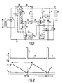
- Circuit d'alimentation pour fournir un courant continu lissé à une impédance de charge (60) comprenant :- des bornes d'entrée (2-1, 2-2) pour recevoir une tension constituée d'une composante de tension continue et d'une composante de tension alternative périodique qui y est superposée, présentant une période d'ondulation spécifiée;- des bornes de sortie (4-1, 4-2) pour connecter l'impédance de charge (60);- un élément en série (10) pouvant être commandé par l'intermédiaire d'une entrée de commande (20) et comportant un trajet de courant principal connecté en série avec l'impédance de charge (60);- un filtre passe-bas (28) comportant une sortie sur laquelle est présente une tension dont la composante de tension continue est déterminée par au moins un condensateur de filtre,- et un amplificateur différentiel (14) comportant une sortie connectée à l'entrée de commande (20) de l'élément en série (10), comportant une première entrée (16) qui est alimentée d'une tension proportionnelle à la tension présente dans l'impédance de charge (10), et comportant une seconde entrée (18) connectée à la sortie du filtre passe-bas,
caractérisé en ce qu'il comprend, en outre :- un moyen de drainage (44, 50) pour drainer le courant du condensateur (30) du filtre, chargeant ainsi ce condensateur pendant au moins une partie de la période d'ondulation;- un moyen d'acheminement de courant (36) pour acheminer du courant au condensateur de filtre (30) de manière à le décharger, le courant acheminé étant important par rapport au courant de drainage;- un circuit à tension de seuil (42) pour produire une tension de seuil,- et un comparateur (42) à alimenter au moyen de la tension de seuil, comportant une entrée (48) à laquelle la tension passant par l'élément en série (10) est appliquée et comportant une sortie connectée au moyen d'acheminement de courant (36) pour faire en sorte que le courant acheminé passe si la tension dans l'élément en série est inférieure à la tension de seuil. - Circuit d'alimentation suivant la revendication 1, caractérisé en ce que le circuit à tension de seuil et le comparateur sont tous deux formés ensemble par un transistor (44) dont la jonction base-émetteur est connectée en parallèle avec le trajet de courant principal de l'élément en série (10), la tension directe de la jonction base-émetteur formant la tension de seuil et le collecteur formant la sortie du comparateur.
- Circuit d'alimentation suivant la revendication 1 ou 2, caractérisé en ce que les moyens d'acheminement de courant (36) sont formés par un montage en série d'une résistance (38) et d'une diode (40), le montage en série étant connecté entre une des bornes d'entrée (2-1) et le condensateur de filtre (30), et le point de jonction de la résistance (38) et de la diode (40) étant connecté à la sortie du comparateur.
- Circuit d'alimentation suivant l'une quelconque des revendications précédentes, caractérisé en ce que l'élément en série (10) est formé par un transistor à effet de champ.
- Circuit d'alimentation suivant l'une quelconque des revendications précédentes, caractérisé en ce que le filtre passe-bas (28) est formé par le circuit parallèle d'un premier condensateur de filtre (30) avec un montage en série d'une résistance (34) et d'un second condensateur de filtre (34), les connexions du premier condensateur de filtre formant l'entrée et les connexions du second condensateur de filtre (32) formant la sortie du filtre (28).
Applications Claiming Priority (2)
| Application Number | Priority Date | Filing Date | Title |
|---|---|---|---|
| NL8601854 | 1986-07-16 | ||
| NL8601854A NL8601854A (nl) | 1986-07-16 | 1986-07-16 | Voedingsschakeling voor het toevoeren van een afgevlakte gelijkstroom aan een belastingsimpedantie. |
Publications (2)
| Publication Number | Publication Date |
|---|---|
| EP0256569A1 EP0256569A1 (fr) | 1988-02-24 |
| EP0256569B1 true EP0256569B1 (fr) | 1992-03-11 |
Family
ID=19848324
Family Applications (1)
| Application Number | Title | Priority Date | Filing Date |
|---|---|---|---|
| EP87201224A Expired EP0256569B1 (fr) | 1986-07-16 | 1987-06-25 | Circuit d'alimentation pour fournir un courant continu lissé à une impédance de charge |
Country Status (7)
| Country | Link |
|---|---|
| US (1) | US4771373A (fr) |
| EP (1) | EP0256569B1 (fr) |
| JP (1) | JPH0783585B2 (fr) |
| CN (1) | CN1009695B (fr) |
| CA (1) | CA1272757A (fr) |
| DE (1) | DE3777285D1 (fr) |
| NL (1) | NL8601854A (fr) |
Families Citing this family (8)
| Publication number | Priority date | Publication date | Assignee | Title |
|---|---|---|---|---|
| US5132894A (en) * | 1990-09-10 | 1992-07-21 | Sundstrand Corporation | Electric power generating system with active damping |
| US5245526A (en) * | 1992-02-07 | 1993-09-14 | Power Integrations, Inc. | Below ground current sensing with current input to control threshold |
| US5450307A (en) * | 1993-02-19 | 1995-09-12 | Sony Corporation | Switching power source apparatus |
| US5469046A (en) * | 1993-04-30 | 1995-11-21 | North American Philips Corporation | Transformerless low voltage switching power supply |
| GB2298531A (en) * | 1995-02-22 | 1996-09-04 | Motorola Ltd | Voltage follower circuit providing filtered output voltage |
| AT405703B (de) * | 1996-07-23 | 1999-11-25 | Siemens Ag Oesterreich | Netzgerät |
| JP2000197365A (ja) * | 1998-12-24 | 2000-07-14 | Denso Corp | 直流電源回路 |
| CN1910818B (zh) * | 2004-01-13 | 2010-06-23 | Nxp股份有限公司 | 高速比较器 |
Family Cites Families (7)
| Publication number | Priority date | Publication date | Assignee | Title |
|---|---|---|---|---|
| US3226630A (en) * | 1963-03-01 | 1965-12-28 | Raytheon Co | Power supply regulators |
| US3354380A (en) * | 1965-12-28 | 1967-11-21 | Bell Telephone Labor Inc | Transistor switching rectifier with controlled conduction |
| US4127895A (en) * | 1977-08-19 | 1978-11-28 | Krueger Paul J | Charge-transfer voltage converter |
| US4341990A (en) * | 1981-04-27 | 1982-07-27 | Motorola, Inc. | High frequency line ripple cancellation circuit |
| SE8106447L (sv) * | 1981-11-02 | 1983-05-03 | Bror Allan Eriksson | Anordning for konstanteffektreglering |
| US4473784A (en) * | 1983-03-14 | 1984-09-25 | Morez Gene S | Power control circuit |
| US4685046A (en) * | 1985-10-03 | 1987-08-04 | The Scott & Fetzer Company | Low voltage direct current power supply |
-
1986
- 1986-07-16 NL NL8601854A patent/NL8601854A/nl not_active Application Discontinuation
-
1987
- 1987-06-25 DE DE8787201224T patent/DE3777285D1/de not_active Expired - Lifetime
- 1987-06-25 EP EP87201224A patent/EP0256569B1/fr not_active Expired
- 1987-07-09 CA CA000541736A patent/CA1272757A/fr not_active Expired
- 1987-07-09 US US07/071,693 patent/US4771373A/en not_active Expired - Fee Related
- 1987-07-13 CN CN87104868.XA patent/CN1009695B/zh not_active Expired
- 1987-07-14 JP JP62174021A patent/JPH0783585B2/ja not_active Expired - Lifetime
Also Published As
| Publication number | Publication date |
|---|---|
| CA1272757A (fr) | 1990-08-14 |
| DE3777285D1 (de) | 1992-04-16 |
| EP0256569A1 (fr) | 1988-02-24 |
| CN87104868A (zh) | 1988-01-27 |
| NL8601854A (nl) | 1988-02-16 |
| JPH0783585B2 (ja) | 1995-09-06 |
| JPS6331469A (ja) | 1988-02-10 |
| CN1009695B (zh) | 1990-09-19 |
| US4771373A (en) | 1988-09-13 |
Similar Documents
| Publication | Publication Date | Title |
|---|---|---|
| US5402059A (en) | Switching power supply operating at little or no load | |
| US5834924A (en) | In-rush current reduction circuit for boost converters and electronic ballasts | |
| EP0500789B1 (fr) | Systeme d'alimentation ininterrompue a circuit ameliore de correction du facteur de puissance | |
| US6051935A (en) | Circuit arrangement for controlling luminous flux produced by a light source | |
| EP0444428B1 (fr) | Alimentation régulée en modulation de largeur d'impulsion comprenant une bobine d'induction avec 3 enroulements | |
| US4652984A (en) | Self-oscillating power-supply circuit | |
| US5712774A (en) | Device for suppressing higher harmonic current of power source | |
| US4939632A (en) | Power supply circuit | |
| JPH06197545A (ja) | スイッチモード電源 | |
| AU696737B2 (en) | High efficiency voltage converter and regulator circuit | |
| US4654538A (en) | Dual input voltage power supply | |
| EP0256569B1 (fr) | Circuit d'alimentation pour fournir un courant continu lissé à une impédance de charge | |
| EP0489477A1 (fr) | Circuit de cmmande de lampes à décharge | |
| EP0054076B1 (fr) | Circuit de decharge pour une source de courant de redressement | |
| EP0507393A2 (fr) | Agencement de circuit | |
| US5828562A (en) | Double discharge circuit for improving the power factor | |
| US5404095A (en) | Mode power supply including self-inductance in the drive circuit | |
| CA1169484A (fr) | Convertisseur de courant continu en courant alternatif | |
| US6473322B2 (en) | AC-DC converter | |
| EP1040729A2 (fr) | Montage de circuit | |
| US5604422A (en) | Transient voltage protection circuit for a DC voltage supply | |
| JPH08221141A (ja) | 電源回路 | |
| US4345200A (en) | Load output level control circuit | |
| JPH0370208A (ja) | ゼロクロス形無接点スイッチ | |
| JPS62210745A (ja) | 雑音遮断回路 |
Legal Events
| Date | Code | Title | Description |
|---|---|---|---|
| PUAI | Public reference made under article 153(3) epc to a published international application that has entered the european phase |
Free format text: ORIGINAL CODE: 0009012 |
|
| AK | Designated contracting states |
Kind code of ref document: A1 Designated state(s): DE FR GB IT SE |
|
| 17P | Request for examination filed |
Effective date: 19880819 |
|
| 17Q | First examination report despatched |
Effective date: 19900829 |
|
| GRAA | (expected) grant |
Free format text: ORIGINAL CODE: 0009210 |
|
| AK | Designated contracting states |
Kind code of ref document: B1 Designated state(s): DE FR GB IT SE |
|
| REF | Corresponds to: |
Ref document number: 3777285 Country of ref document: DE Date of ref document: 19920416 |
|
| ITF | It: translation for a ep patent filed | ||
| ET | Fr: translation filed | ||
| PLBE | No opposition filed within time limit |
Free format text: ORIGINAL CODE: 0009261 |
|
| STAA | Information on the status of an ep patent application or granted ep patent |
Free format text: STATUS: NO OPPOSITION FILED WITHIN TIME LIMIT |
|
| 26N | No opposition filed | ||
| ITTA | It: last paid annual fee | ||
| EAL | Se: european patent in force in sweden |
Ref document number: 87201224.0 |
|
| ITPR | It: changes in ownership of a european patent |
Owner name: CAMBIO RAGIONE SOCIALE;PHILIPS ELECTRONICS N.V. |
|
| REG | Reference to a national code |
Ref country code: FR Ref legal event code: CD |
|
| REG | Reference to a national code |
Ref country code: FR Ref legal event code: CD |
|
| PGFP | Annual fee paid to national office [announced via postgrant information from national office to epo] |
Ref country code: GB Payment date: 19990621 Year of fee payment: 13 |
|
| PGFP | Annual fee paid to national office [announced via postgrant information from national office to epo] |
Ref country code: SE Payment date: 19990624 Year of fee payment: 13 |
|
| PGFP | Annual fee paid to national office [announced via postgrant information from national office to epo] |
Ref country code: FR Payment date: 19990628 Year of fee payment: 13 |
|
| PGFP | Annual fee paid to national office [announced via postgrant information from national office to epo] |
Ref country code: DE Payment date: 19990722 Year of fee payment: 13 |
|
| PG25 | Lapsed in a contracting state [announced via postgrant information from national office to epo] |
Ref country code: GB Free format text: LAPSE BECAUSE OF NON-PAYMENT OF DUE FEES Effective date: 20000625 |
|
| PG25 | Lapsed in a contracting state [announced via postgrant information from national office to epo] |
Ref country code: SE Free format text: LAPSE BECAUSE OF NON-PAYMENT OF DUE FEES Effective date: 20000626 |
|
| GBPC | Gb: european patent ceased through non-payment of renewal fee |
Effective date: 20000625 |
|
| EUG | Se: european patent has lapsed |
Ref document number: 87201224.0 |
|
| PG25 | Lapsed in a contracting state [announced via postgrant information from national office to epo] |
Ref country code: FR Free format text: LAPSE BECAUSE OF NON-PAYMENT OF DUE FEES Effective date: 20010228 |
|
| REG | Reference to a national code |
Ref country code: FR Ref legal event code: ST |
|
| PG25 | Lapsed in a contracting state [announced via postgrant information from national office to epo] |
Ref country code: DE Free format text: LAPSE BECAUSE OF NON-PAYMENT OF DUE FEES Effective date: 20010403 |
|
| PG25 | Lapsed in a contracting state [announced via postgrant information from national office to epo] |
Ref country code: IT Free format text: LAPSE BECAUSE OF NON-PAYMENT OF DUE FEES Effective date: 20050625 |