EP0257119A1 - Integriertes Verdrahtungssystem für sehr hochintegrierte Schaltungen - Google Patents
Integriertes Verdrahtungssystem für sehr hochintegrierte Schaltungen Download PDFInfo
- Publication number
- EP0257119A1 EP0257119A1 EP86111642A EP86111642A EP0257119A1 EP 0257119 A1 EP0257119 A1 EP 0257119A1 EP 86111642 A EP86111642 A EP 86111642A EP 86111642 A EP86111642 A EP 86111642A EP 0257119 A1 EP0257119 A1 EP 0257119A1
- Authority
- EP
- European Patent Office
- Prior art keywords
- wiring
- wafer
- wiring system
- interconnection
- chip
- Prior art date
- Legal status (The legal status is an assumption and is not a legal conclusion. Google has not performed a legal analysis and makes no representation as to the accuracy of the status listed.)
- Granted
Links
Images



Classifications
-
- H—ELECTRICITY
- H10—SEMICONDUCTOR DEVICES; ELECTRIC SOLID-STATE DEVICES NOT OTHERWISE PROVIDED FOR
- H10W—GENERIC PACKAGES, INTERCONNECTIONS, CONNECTORS OR OTHER CONSTRUCTIONAL DETAILS OF DEVICES COVERED BY CLASS H10
- H10W70/00—Package substrates; Interposers; Redistribution layers [RDL]
- H10W70/60—Insulating or insulated package substrates; Interposers; Redistribution layers
- H10W70/611—Insulating or insulated package substrates; Interposers; Redistribution layers for connecting multiple chips together
-
- H—ELECTRICITY
- H10—SEMICONDUCTOR DEVICES; ELECTRIC SOLID-STATE DEVICES NOT OTHERWISE PROVIDED FOR
- H10W—GENERIC PACKAGES, INTERCONNECTIONS, CONNECTORS OR OTHER CONSTRUCTIONAL DETAILS OF DEVICES COVERED BY CLASS H10
- H10W70/00—Package substrates; Interposers; Redistribution layers [RDL]
- H10W70/60—Insulating or insulated package substrates; Interposers; Redistribution layers
- H10W70/62—Insulating or insulated package substrates; Interposers; Redistribution layers characterised by their interconnections
- H10W70/63—Vias, e.g. via plugs
- H10W70/635—Through-vias
-
- H—ELECTRICITY
- H10—SEMICONDUCTOR DEVICES; ELECTRIC SOLID-STATE DEVICES NOT OTHERWISE PROVIDED FOR
- H10W—GENERIC PACKAGES, INTERCONNECTIONS, CONNECTORS OR OTHER CONSTRUCTIONAL DETAILS OF DEVICES COVERED BY CLASS H10
- H10W70/00—Package substrates; Interposers; Redistribution layers [RDL]
- H10W70/60—Insulating or insulated package substrates; Interposers; Redistribution layers
- H10W70/67—Insulating or insulated package substrates; Interposers; Redistribution layers characterised by their insulating layers or insulating parts
- H10W70/69—Insulating materials thereof
- H10W70/698—Semiconductor materials that are electrically insulating, e.g. undoped silicon
-
- H—ELECTRICITY
- H10—SEMICONDUCTOR DEVICES; ELECTRIC SOLID-STATE DEVICES NOT OTHERWISE PROVIDED FOR
- H10W—GENERIC PACKAGES, INTERCONNECTIONS, CONNECTORS OR OTHER CONSTRUCTIONAL DETAILS OF DEVICES COVERED BY CLASS H10
- H10W90/00—Package configurations
-
- H—ELECTRICITY
- H10—SEMICONDUCTOR DEVICES; ELECTRIC SOLID-STATE DEVICES NOT OTHERWISE PROVIDED FOR
- H10W—GENERIC PACKAGES, INTERCONNECTIONS, CONNECTORS OR OTHER CONSTRUCTIONAL DETAILS OF DEVICES COVERED BY CLASS H10
- H10W90/00—Package configurations
- H10W90/20—Configurations of stacked chips
- H10W90/28—Configurations of stacked chips the stacked chips having different sizes, e.g. chip stacks having a pyramidal shape
-
- H—ELECTRICITY
- H10—SEMICONDUCTOR DEVICES; ELECTRIC SOLID-STATE DEVICES NOT OTHERWISE PROVIDED FOR
- H10W—GENERIC PACKAGES, INTERCONNECTIONS, CONNECTORS OR OTHER CONSTRUCTIONAL DETAILS OF DEVICES COVERED BY CLASS H10
- H10W90/00—Package configurations
- H10W90/401—Package configurations characterised by multiple insulating or insulated package substrates, interposers or RDLs
-
- H—ELECTRICITY
- H10—SEMICONDUCTOR DEVICES; ELECTRIC SOLID-STATE DEVICES NOT OTHERWISE PROVIDED FOR
- H10W—GENERIC PACKAGES, INTERCONNECTIONS, CONNECTORS OR OTHER CONSTRUCTIONAL DETAILS OF DEVICES COVERED BY CLASS H10
- H10W72/00—Interconnections or connectors in packages
- H10W72/071—Connecting or disconnecting
- H10W72/072—Connecting or disconnecting of bump connectors
- H10W72/07251—Connecting or disconnecting of bump connectors characterised by changes in properties of the bump connectors during connecting
-
- H—ELECTRICITY
- H10—SEMICONDUCTOR DEVICES; ELECTRIC SOLID-STATE DEVICES NOT OTHERWISE PROVIDED FOR
- H10W—GENERIC PACKAGES, INTERCONNECTIONS, CONNECTORS OR OTHER CONSTRUCTIONAL DETAILS OF DEVICES COVERED BY CLASS H10
- H10W72/00—Interconnections or connectors in packages
- H10W72/20—Bump connectors, e.g. solder bumps or copper pillars; Dummy bumps; Thermal bumps
-
- H—ELECTRICITY
- H10—SEMICONDUCTOR DEVICES; ELECTRIC SOLID-STATE DEVICES NOT OTHERWISE PROVIDED FOR
- H10W—GENERIC PACKAGES, INTERCONNECTIONS, CONNECTORS OR OTHER CONSTRUCTIONAL DETAILS OF DEVICES COVERED BY CLASS H10
- H10W72/00—Interconnections or connectors in packages
- H10W72/50—Bond wires
- H10W72/531—Shapes of wire connectors
- H10W72/5363—Shapes of wire connectors the connected ends being wedge-shaped
Definitions
- This invention relates generally to the field of integrated circuit chip packaging and more particularly to a VLSI (very large scale integration) adequate packaging concept using substrates of semiconductor material for superior chip or component interconnection.
- VLSI very large scale integration
- the proposed integrated silicon based packaging/wiring concept provides for the VLSI chips to be placed within corresponding openings of somewhat larger size in a silicon interconnection wafer (IW) supported by a carrier structure.
- the interconnection wafer bears multilevel (ML) wiring planes and has incorporated circuit components integrated in a less demanding technology, say, in 5 ⁇ m technology, as compared to, say, in 1 ⁇ m technology of the VLSI chips.
- Silicon contact chips with conductive surface layers placed over the chip/IW plane provide for the required contacts or interconnection by means of needle-like structures inserted in corresponding via holes which needles are better suited as to shear strain problems otherwise encountered with conventional C-4 (Controlled Collapse Chip Connection) joints; consequently a much higher number of chip pads can be allowed with almost no restrictions as to where they have to be located.
- Power is supplied via rather large-dimensioned conductive planes, e.g. in the form of Cu rails, running within the carrier and surfacing stud-like in the peripheral region of said openings in the interconnection wafer for further distribution via the contact chip. All components of this wiring system are laid out taking advantage of modern silicon (generally semiconductor) micro-machining methods resulting in a superior VLSI adequate packaging concept.
- FIG.1 the major elements of the proposed package are illustrated in a rather simplified exploded view to facilitate overall understanding of the relative part positions and the resulting package assembly.
- carrier 1 Onto carrier 1 there is attached interconnection wafer 2 (later also referred to as IW) with openings 3 into which VLSI chips 4 are placed “backside down", i.e. the "active" side is up.
- IW 2 and VLSI chips 4 are eventually held in intimate contact with carrier 1 for efficient heat transfer which is generally indicated by the cooling fins.
- the slots shown in the carrier substrate are for the buried power supply rails (not shown) to surface; this is described in greater detail below with reference to Fig.2, 5 and 7.
- Interconnection between the VLSI chips and the IW is made by means of special contact chips 5 which have formed on their surfaces power and signal wiring levels and which are equipped with needle-like contacts inserted through corresponding vias; again a more detailed description is given with reference to Figs. 2, 6B, 8 and 9.
- another wiring level may be added in the form of a high performance wiring wafer (HPWW) 6 which is described in greater detail with reference to Figs. 2 and 10.
- HPWW high performance wiring wafer
- Openings 7 may be provided in the HPWW 6 at the location of the VLSI chips for testing and repair purposes.
- the IW 2 - like the VLSI chips 4 - consists of monocrystalline semiconductor material suitable for integrated ciruit manufacturing. Typically this will be silicon but it may be also advantageous to have some of the VLSI chips along a critical timing path under system aspects formed as, for instance, fast GaAs IC's.
- the contact chips as well as the HPWW 6 (if any) and preferably the carrier should be of a material which allows application of the silicon micro-machining methods which have become quite attractive for achieving extraordinary small and precise mechanical microstructures and for which reference is made to the prior art listed in section c) above.
- the carrier material may be also selected from other material groups such as copper, silicon carbide, ceramic or the like depending upon the specific emphasis placed on a particular function, for instance, minimum thermal mismatch relative to the IW or maximum cooling capacity or electrical conductivity; for the latter an example is described below with reference to Fig. 5.
- the wiring package described so far may be completed by attaching it to a conventional MLC (multilayer ceramic) frame 8 with I/O pins and finally providing a sealing cover, for instance, by twin cap 9 with external power connections by an outer ground (GND) cap and an inner supply voltage cap, e.g. for +V.
- MLC multilayer ceramic
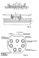
- Fig. 2 shows in greater detail sectional views of different magnification through the proposed packaging and wiring system which, in addition to Fig. 1, are to aid understanding of the "in-place" packaging configuration.
- Carrier 1 contains the low-ohmic buried power supply line system indicated by power rails 20 which - at the periphery of the opening in the IW 2 for accomodation of the VLSI chip 4 - extend (as studs 21) to the surface for further connection as shown.
- specific contact chips (CC) 5 are provided in a wiring plane overlying the IW level.
- the surfaces of contact chips 5 are covered with conductive layers 22 and 23 serving as, for instance, power and signal distribution planes, respectively, and working in connection with corresponding contact needles 24.
- HPWW 6 (mentioned earlier) which is structured similar to the CC 5. From Fig. 2 it can further be seen that the provision of openings 25 in HPWW 6 allows for elegant in-place testability of chips 4 since contact needles 24 "extend" the chip pads to the upper surface of CC 5 so that they become “externally” accessible.
- Fig. 3 is a schematical representation of interconnection wafer (IW) 2 with specific emphasis given to the type of its incorporated circuit and wiring elements.
- IW interconnection wafer
- Fig. 4 gives an example of a typical structure crossection from which it is apparent that IW 2 and VLSI chip 4 have in common that they both are integrated circuit structures but with certain modifications.
- a specifically important feature of the proposed wiring system is that the IW 2 for its (driver) circuit and other wiring elements takes advantage of the substantially higher yield when allowing a less aggressive or demanding integration technology.
- Fig. 3 shows as a full circular shaped wafer this is, of course, not necessary in all cases.
- Fig. 1 shows as another example a rectangular IW form. Further shapes for the IW are also possible depending on specific application contexts, e.g. a cross-like IW structure etc.
- Fig. 4 is to illustrate what the internal layer structure of the interconnection wafer and a VLSI chip could be.
- the embodiment of Fig. 4 would be typical for a bipolar technology.
- Both the VLSI chip and the IW have an epitaxial layer (EPI) formed on a monocrystalline silicon (generallyly: semiconductor) substrate.
- EPI epitaxial layer
- the epitaxial layer there are formed in conventional manner the required integrated circuit elements, for instance, in the IW a transistor driver stage with 41, 42 and 43 representing the base, emitter and collector (contact) regions of the specific conductivity types required.
- the isolation (ISO) may be of any conventional type such as electric, dielectric or a combination of both.
- the IW has provided three conductive layers (1L, 2L, 3L) for the wiring whereas the VLSI chip has two of those.
- the wiring layers are separated by a suitable dielectric such as SiO2, Si3N4, polyimide (PI) or combinations thereof.
- PI polyimide
- Indicated by an interrupted line is a wiring connection between two pads of the VLSI chip and the interconnection wafer for which interconnection a preferred implementation is proposed by the invention in the form of the contact chip.
- PI polyimide
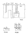
- Figs. 5, 6 and 7 the power supply system is described in greater detail.
- GND and +V two separate power rails
- a highly conductive carrier e.g. made of copper
- it may be advantageous to use the carrier for supplying the GND potential so that merely one power rail (for + V) needs to be provided in a correspondingly smaller slot 51 as is indicated in the left part of Fig. 5.
- the crossection of the power rails in Fig. 5 can be as large as 5 mm (height) by 0.5 mm (width).
- the power rails are to be isolated against each other or against the substrate which can be done by a variety of conventional ways such as embedding them in suitable dielectric material etc.
- additional decoupling capacitors may be provided, (if required) as illustrated generally by C B .
- the buried power rails preferably protrude from the carrier 1 up to the level of the chip and/or IW surface. Connection can thus be made between pads in the same (height) level.
- Figs. 6A, B show - in enlarged form - examples for such a connection for the detail area indicated with 6AB in Fig. 5. While suitable connections may be made in a great variety of conventional ways, e.g. by wire or flex tab bonds 60 (Fig. 6A) the preferred way is that illustrated in Fig. 6B, i.e. by means of a contact chip 5 (already mentioned above) having inserted contact needles 61 and 62.
- the example shows a connection between carrier 1 and the VLSI chip 4.
- Contact needle 61 contacts (a pad on) carrier 1; via the solder joint 63 to metal layer 22 and further solder joint 64 connection is made to contact needle 62 and to chip pad 65.
- solder rings 66 and 67 on the upper surface of contact chip 5 are isolated from the remaining layer on that surface.
- FIG. 6A and 6B show connections established between the carrier substrate and a chip this is, of course, for illustration purposes only. Other interconnections can be provided in the same manner.
- Fig. 7 gives a rather schematical survey of some interconnections provided between VLSI chip 4 placed in opening 3 (periphery 70) of IW 2 together with power rails 71, 72, 73 and 74. It is to be understood that these interconnections are most preferably made by means of a contact chip which has been shown in earlier Figs. 1,2, 5 and 6B and which will be described in some more detail below.
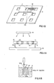
- Figs. 8A and 8B show in diagrammatical and crossectional view the body of a contact chip 5; Fig. 9 is to illustrate how the contact chip 5 establishes the desired connections between corresponding chip and/or wiring wafer pads.
- Contact chip 5 has formed in its body via holes, e.g. 80, 81 in Fig. 8B, with a typical diameter of about 100 ⁇ m.
- Rings 82 and 83 of a solder material are provided around the periphery of via holes 80, 81 on the top and bottom surface of contact chip 5.
- Solder rings 82 and 83 are preferably formed by conventional evaporation of PbSn with a thickness of about 20 to 50 ⁇ m.
- solder rings are physically connected to the remaining interconnection pattern formed in that particular surface wiring level, i.e. in the signal distribution plane 84 or in the power distribution plane 85.
- These wiring planes may be of conventional Al-Cu or other suitable material of good electrical conductivity.
- the signal distribution plane 84 on upper surface of contact chip 5 this is shown in Fig. 9.
- the openings in solder rings are of a smaller dimension compared to the diameter of the associated via holes 80 and 81 so that there exist PbSn overhangs indicated, for instance, in Fig. 8B as 86 and 87.
- contact needles are inserted into the via holes of contact chip 5.
- Suitable materials for the contact needles may include V2A steel, tungsten etc. being coated with (electroless) solder material such as PbSn.
- the final arrangement may best be understood with further reference to Fig. 9.
- contact needles 90 are held by means of the two "soft" solder rings per via hole, such as rings 82 and 83 of via hole 80 in Fig. 8B.
- contact needles 90 allow for an adjustment in their vertical direction so that reliable contacts are made even to pads of varying heights.
- Fig. 9 illustrates this adjustment capability for different chip pad elevations by corresponding arrows. Compared to Fig.
- Fig. 9 the representation of Fig. 9 is further completed with regard to the interconnections made between (some of) the contact needles and the (signal) wiring pattern on the (upper) surface shown. Needles which are not connected in this upper surface of contact chip 5 are connected to the (power) wiring plane on the bottom surface (not shown) of contact chip 5. A preferred way of forming the contact chip body with its precise hole pattern is described below with reference to Fig. 11.
- Fig. 10 shows again the afore-mentioned high performance wiring wafer (HPWW) 6 which may be added to the proposed wiring scheme, if there is a need for additional low-ohmic and low-capacitance interconnection facilities.
- openings 7 reference 100 is to indicate groups of holes with contact needles of the type described above. These needles reach down to corresponding pads on the interconnection wafer (referred to as 2 in earlier Figs. 1 and 2) and may be selectively connected on this HPWW packaging level to the respective wiring pattern.
- the wiring planes of the HPWW 6 are preferably organized as, for instance, an X-wiring plane on the upper surface shown in Fig. 10 and an Y-wiring plane on its bottom surface.
- Indicated as 101 in Fig. 10 is a group of rather “large” (about 100 ⁇ m) conductive lines running in the X-direction and being connected to corresponding contact needles in the same way as shown earlier for the contact chip.
- the described wiring scheme allows for optimum interconnection of VLSI chips in a "VLSI adequate" packaging system. In particular, it allows for consideration of different interconnection lengths as well as loads due to different fan-in and/or fan-out figures. For instance, connecting an output of a first VLSI- chip via a single line to an input of another chip may be done best via the interconnection wafer level. However, if several chip inputs are to be coupled to one output on another chip or if a rather long interconnection is to be provided, then going via the HPWW may be the preferable way.
- a typical hierarchy order with regard to the corresponding line width used in the proposed wiring system may be as follows: VLSI chip 1 ⁇ m IW, CC 10 ⁇ m HPWW 100 ⁇ m MLC 1000 ⁇ m
- resulting packaging further allows for accomodation of VLSI chips of different circuit and technology type such as MOS/CMOS/ECL/GaAs etc.
- a preferred way is described to form a very precise via hole pattern in the contact chip and high performance wiring wafer to the required quality.
- Silicon wafer 110 of a ⁇ 100 > crystal orientation and having Al dots 111 (with a typical diameter of 100 ⁇ m and a thickness of 20 to 30 ⁇ m) evaporated onto one of its surfaces is placed over water cooled plate 112 by means of quartz spacers 113.
- Infrared lamps 114 may be used to heat wafer 110 to a temperature T1 of about 1150° C. Thereby a temperature gradient of about 200° C/cm is generated between the two wafer surfaces.
- T1 of 1150° C T2 will be about 1140° C.
- Al dots 111 migrate to the higher temperature surface (indicated by arrows) and thus form a P+ doping channel or column indicated by reference numeral 115, the doping concentration being typically about 2 ⁇ 1019 Al atoms/cm3.
- the time duration of this thermomigration is only about 5 minutes.
- the wafers are etched as shown in Fig. 11B in a solution comprising (in a part ratio of 1:3:8): HF(50%):HNO3(70%):CH3COOH(99.5%)
Landscapes
- Internal Circuitry In Semiconductor Integrated Circuit Devices (AREA)
Priority Applications (4)
| Application Number | Priority Date | Filing Date | Title |
|---|---|---|---|
| DE8686111642T DE3677601D1 (de) | 1986-08-22 | 1986-08-22 | Integriertes verdrahtungssystem fuer sehr hochintegrierte schaltungen. |
| EP86111642A EP0257119B1 (de) | 1986-08-22 | 1986-08-22 | Integriertes Verdrahtungssystem für sehr hochintegrierte Schaltungen |
| JP62112681A JPS6353960A (ja) | 1986-08-22 | 1987-05-11 | 集積回路チップ用配線システム |
| US07/070,265 US4802062A (en) | 1986-08-22 | 1987-07-06 | Integrated wiring system for VLSI |
Applications Claiming Priority (1)
| Application Number | Priority Date | Filing Date | Title |
|---|---|---|---|
| EP86111642A EP0257119B1 (de) | 1986-08-22 | 1986-08-22 | Integriertes Verdrahtungssystem für sehr hochintegrierte Schaltungen |
Publications (2)
| Publication Number | Publication Date |
|---|---|
| EP0257119A1 true EP0257119A1 (de) | 1988-03-02 |
| EP0257119B1 EP0257119B1 (de) | 1991-02-20 |
Family
ID=8195359
Family Applications (1)
| Application Number | Title | Priority Date | Filing Date |
|---|---|---|---|
| EP86111642A Expired - Lifetime EP0257119B1 (de) | 1986-08-22 | 1986-08-22 | Integriertes Verdrahtungssystem für sehr hochintegrierte Schaltungen |
Country Status (4)
| Country | Link |
|---|---|
| US (1) | US4802062A (de) |
| EP (1) | EP0257119B1 (de) |
| JP (1) | JPS6353960A (de) |
| DE (1) | DE3677601D1 (de) |
Cited By (6)
| Publication number | Priority date | Publication date | Assignee | Title |
|---|---|---|---|---|
| FR2647961A1 (fr) * | 1989-05-30 | 1990-12-07 | Thomson Composants Militaires | Circuit electronique a plusieurs puces, en boitier ceramique avec puce d'interconnexion |
| EP0516875A1 (de) * | 1991-06-06 | 1992-12-09 | International Business Machines Corporation | Elektronischer Packungsmodul |
| EP0547807A3 (en) * | 1991-12-16 | 1993-09-22 | General Electric Company | Packaged electronic system |
| US5359496A (en) * | 1989-12-21 | 1994-10-25 | General Electric Company | Hermetic high density interconnected electronic system |
| FR2704690A1 (fr) * | 1993-04-27 | 1994-11-04 | Thomson Csf | Procédé d'encapsulation de pastilles semi-conductrices, dispositif obtenu par ce procédé et application à l'interconnexion de pastilles en trois dimensions. |
| WO2004112136A1 (en) * | 2003-06-12 | 2004-12-23 | Koninklijke Philips Electronics N.V. | Electronic device |
Families Citing this family (20)
| Publication number | Priority date | Publication date | Assignee | Title |
|---|---|---|---|---|
| US5007841A (en) * | 1983-05-31 | 1991-04-16 | Trw Inc. | Integrated-circuit chip interconnection system |
| US5182420A (en) * | 1989-04-25 | 1993-01-26 | Cray Research, Inc. | Method of fabricating metallized chip carriers from wafer-shaped substrates |
| US5150196A (en) * | 1989-07-17 | 1992-09-22 | Hughes Aircraft Company | Hermetic sealing of wafer scale integrated wafer |
| JPH0384804A (ja) * | 1989-08-25 | 1991-04-10 | Masaru Minagawa | 植物を利用した台座の製造方法 |
| US5119273A (en) * | 1990-01-29 | 1992-06-02 | The United States Of America As Represented By The Secretary Of The Navy | High speed parallel backplane |
| US5120572A (en) * | 1990-10-30 | 1992-06-09 | Microelectronics And Computer Technology Corporation | Method of fabricating electrical components in high density substrates |
| US5254493A (en) * | 1990-10-30 | 1993-10-19 | Microelectronics And Computer Technology Corporation | Method of fabricating integrated resistors in high density substrates |
| US5130768A (en) * | 1990-12-07 | 1992-07-14 | Digital Equipment Corporation | Compact, high-density packaging apparatus for high performance semiconductor devices |
| US5196377A (en) * | 1990-12-20 | 1993-03-23 | Cray Research, Inc. | Method of fabricating silicon-based carriers |
| US5508938A (en) * | 1992-08-13 | 1996-04-16 | Fujitsu Limited | Special interconnect layer employing offset trace layout for advanced multi-chip module packages |
| US5719748A (en) * | 1995-06-28 | 1998-02-17 | Honeywell Inc. | Semiconductor package with a bridge for chip area connection |
| US6713854B1 (en) | 2000-10-16 | 2004-03-30 | Legacy Electronics, Inc | Electronic circuit module with a carrier having a mounting pad array |
| US7102892B2 (en) * | 2000-03-13 | 2006-09-05 | Legacy Electronics, Inc. | Modular integrated circuit chip carrier |
| US7337522B2 (en) * | 2000-10-16 | 2008-03-04 | Legacy Electronics, Inc. | Method and apparatus for fabricating a circuit board with a three dimensional surface mounted array of semiconductor chips |
| CN100369536C (zh) * | 2001-03-14 | 2008-02-13 | 莱格西电子股份有限公司 | 制造具有三维半导体芯片阵列安装面的电路板的方法和装置 |
| US7435097B2 (en) * | 2005-01-12 | 2008-10-14 | Legacy Electronics, Inc. | Radial circuit board, system, and methods |
| CN107770956A (zh) * | 2016-08-16 | 2018-03-06 | 光宝电子(广州)有限公司 | 电路板结构 |
| US10985103B2 (en) | 2019-03-01 | 2021-04-20 | Samsung Electronics Co., Ltd | Apparatus and method of forming backside buried conductor in integrated circuit |
| US10886224B2 (en) | 2019-05-22 | 2021-01-05 | Samsung Electronics Co., Ltd. | Power distribution network using buried power rail |
| US11233008B2 (en) | 2019-06-19 | 2022-01-25 | Samsung Electronics Co., Ltd. | Method of manufacturing an integrated circuit with buried power rail |
Citations (4)
| Publication number | Priority date | Publication date | Assignee | Title |
|---|---|---|---|---|
| US3777221A (en) * | 1972-12-18 | 1973-12-04 | Ibm | Multi-layer circuit package |
| FR2295570A1 (fr) * | 1974-12-20 | 1976-07-16 | Ibm | Assemblage electrique pour circuits integres et son procede de montage |
| DE3511722A1 (de) * | 1984-04-02 | 1985-10-03 | Burroughs Corp. (n.d. Ges. des Staates Delaware), Detroit, Mich. | Elektromechanische baugruppe fuer integrierte schaltkreismatrizen |
| FR2569052A1 (fr) * | 1984-08-10 | 1986-02-14 | Thomson Csf | Procede d'interconnexion de circuits integres |
Family Cites Families (9)
| Publication number | Priority date | Publication date | Assignee | Title |
|---|---|---|---|---|
| JPS5423484A (en) * | 1977-07-25 | 1979-02-22 | Hitachi Ltd | Semiconductor integrated circuit and its manufacture |
| US4288841A (en) * | 1979-09-20 | 1981-09-08 | Bell Telephone Laboratories, Incorporated | Double cavity semiconductor chip carrier |
| US4328530A (en) * | 1980-06-30 | 1982-05-04 | International Business Machines Corporation | Multiple layer, ceramic carrier for high switching speed VLSI chips |
| US4445112A (en) * | 1980-12-12 | 1984-04-24 | Bei Electronics, Inc. | Positional encoders with plug-together modules |
| US4598337A (en) * | 1984-09-17 | 1986-07-01 | Timex Corporation | Electronic circuit board for a timepiece |
| US4645943A (en) * | 1984-10-15 | 1987-02-24 | Dallas Semiconductor Corporation | Space-saving back-up power supply |
| JPS61107658A (ja) * | 1984-10-31 | 1986-05-26 | Canon Inc | 電子機器 |
| US4705917A (en) * | 1985-08-27 | 1987-11-10 | Hughes Aircraft Company | Microelectronic package |
| US4688151A (en) * | 1986-03-10 | 1987-08-18 | International Business Machines Corporation | Multilayered interposer board for powering high current chip modules |
-
1986
- 1986-08-22 DE DE8686111642T patent/DE3677601D1/de not_active Expired - Lifetime
- 1986-08-22 EP EP86111642A patent/EP0257119B1/de not_active Expired - Lifetime
-
1987
- 1987-05-11 JP JP62112681A patent/JPS6353960A/ja active Granted
- 1987-07-06 US US07/070,265 patent/US4802062A/en not_active Expired - Fee Related
Patent Citations (4)
| Publication number | Priority date | Publication date | Assignee | Title |
|---|---|---|---|---|
| US3777221A (en) * | 1972-12-18 | 1973-12-04 | Ibm | Multi-layer circuit package |
| FR2295570A1 (fr) * | 1974-12-20 | 1976-07-16 | Ibm | Assemblage electrique pour circuits integres et son procede de montage |
| DE3511722A1 (de) * | 1984-04-02 | 1985-10-03 | Burroughs Corp. (n.d. Ges. des Staates Delaware), Detroit, Mich. | Elektromechanische baugruppe fuer integrierte schaltkreismatrizen |
| FR2569052A1 (fr) * | 1984-08-10 | 1986-02-14 | Thomson Csf | Procede d'interconnexion de circuits integres |
Non-Patent Citations (5)
| Title |
|---|
| IBM TECHNICAL DISCLOSURE BULLETIN, vol. 27, no. 6, November 1984, pages 3335-3336, New York, US; L.S. GOLDMANN: "Universal electronic package" * |
| IBM TECHNICAL DISCLOSURE BULLETIN, vol. 28, no. 2, July 1985, pages 811-812, New York, US; "Mated array chip configuration" * |
| IEEE TRANSACTIONS ON COMPONENTS, HYBRIDS AND MANUFACTURING TECHNOLOGY, vol. CHMT-7, no. 2, June 1984, pages 193-196, IEEE, New York, US; R.K. SPIELBERGER et al.: "Silicon-on-silicon packaging" * |
| PATENT ABSTRACTS OF JAPAN, vol. 9, no. 140 (E-321)[1863], 14th June 1985; & JP-A-60 22 352 (TOSHIBA K.K.) 04-02-1985 * |
| PROCEEDINGS OF THE IEEE, vol. 70, no. 5, May 1982, pages 420-457, IEEE, New York, US; K.E. PETERSEN: "Silicon as a mechanical material" * |
Cited By (9)
| Publication number | Priority date | Publication date | Assignee | Title |
|---|---|---|---|---|
| FR2647961A1 (fr) * | 1989-05-30 | 1990-12-07 | Thomson Composants Militaires | Circuit electronique a plusieurs puces, en boitier ceramique avec puce d'interconnexion |
| US5359496A (en) * | 1989-12-21 | 1994-10-25 | General Electric Company | Hermetic high density interconnected electronic system |
| EP0516875A1 (de) * | 1991-06-06 | 1992-12-09 | International Business Machines Corporation | Elektronischer Packungsmodul |
| US5306866A (en) * | 1991-06-06 | 1994-04-26 | International Business Machines Corporation | Module for electronic package |
| EP0547807A3 (en) * | 1991-12-16 | 1993-09-22 | General Electric Company | Packaged electronic system |
| US5315486A (en) * | 1991-12-16 | 1994-05-24 | General Electric Company | Hermetically packaged HDI electronic system |
| FR2704690A1 (fr) * | 1993-04-27 | 1994-11-04 | Thomson Csf | Procédé d'encapsulation de pastilles semi-conductrices, dispositif obtenu par ce procédé et application à l'interconnexion de pastilles en trois dimensions. |
| WO1994025987A1 (fr) * | 1993-04-27 | 1994-11-10 | Thomson-Csf | Procede d'encapsulation de pastilles semi-conductrices, dispositif obtenu par ce procede et application a l'interconnexion de pastilles en trois dimensions |
| WO2004112136A1 (en) * | 2003-06-12 | 2004-12-23 | Koninklijke Philips Electronics N.V. | Electronic device |
Also Published As
| Publication number | Publication date |
|---|---|
| DE3677601D1 (de) | 1991-03-28 |
| EP0257119B1 (de) | 1991-02-20 |
| JPS6353960A (ja) | 1988-03-08 |
| US4802062A (en) | 1989-01-31 |
| JPH0240219B2 (de) | 1990-09-10 |
Similar Documents
| Publication | Publication Date | Title |
|---|---|---|
| EP0257119B1 (de) | Integriertes Verdrahtungssystem für sehr hochintegrierte Schaltungen | |
| CN112514062B (zh) | 具有在芯片与封装衬底之间提供电源连接的芯片互连桥的多芯片封装结构 | |
| CN110676223B (zh) | 封装件和形成封装件的方法 | |
| US6627998B1 (en) | Wafer scale thin film package | |
| KR100656218B1 (ko) | 반도체 또는 유전체 웨이퍼 상에 제조된 패키지 상의 시스템 | |
| US6962867B2 (en) | Methods of fabrication of semiconductor dice having back side redistribution layer accessed using through-silicon vias and assemblies thereof | |
| US6379982B1 (en) | Wafer on wafer packaging and method of fabrication for full-wafer burn-in and testing | |
| US5222014A (en) | Three-dimensional multi-chip pad array carrier | |
| US6437990B1 (en) | Multi-chip ball grid array IC packages | |
| US5016087A (en) | Integrated circuit package | |
| US8501622B2 (en) | Semiconductor device with two or more bond pad connections for each input/output cell and method of manufacture thereof | |
| US6075711A (en) | System and method for routing connections of integrated circuits | |
| US7122904B2 (en) | Semiconductor packaging device and manufacture thereof | |
| US5751554A (en) | Testable chip carrier | |
| KR20000005670A (ko) | 칩-온-칩패키지및그제조방법 | |
| JP2001507520A (ja) | 集積回路パッケージングのための構造体及び方法 | |
| KR20230044308A (ko) | 매우 미세한 피치 및 배선 밀도의 나란한 유기 칩렛 집적 | |
| US6903458B1 (en) | Embedded carrier for an integrated circuit chip | |
| US20250391789A1 (en) | Double seal ring and electrical connection of multiple chiplets | |
| KR100357803B1 (ko) | 다중 칩 패키지 제조 방법 | |
| US6400575B1 (en) | Integrated circuits packaging system and method | |
| US20250219022A1 (en) | Embedded active chip within interposer | |
| WO2000019531A1 (en) | Backside electrical contact structure for a module having an exposed backside |
Legal Events
| Date | Code | Title | Description |
|---|---|---|---|
| PUAI | Public reference made under article 153(3) epc to a published international application that has entered the european phase |
Free format text: ORIGINAL CODE: 0009012 |
|
| AK | Designated contracting states |
Kind code of ref document: A1 Designated state(s): DE FR GB IT |
|
| 17P | Request for examination filed |
Effective date: 19880616 |
|
| 17Q | First examination report despatched |
Effective date: 19891114 |
|
| GRAA | (expected) grant |
Free format text: ORIGINAL CODE: 0009210 |
|
| AK | Designated contracting states |
Kind code of ref document: B1 Designated state(s): DE FR GB IT |
|
| PG25 | Lapsed in a contracting state [announced via postgrant information from national office to epo] |
Ref country code: IT Free format text: LAPSE BECAUSE OF FAILURE TO SUBMIT A TRANSLATION OF THE DESCRIPTION OR TO PAY THE FEE WITHIN THE PRE;WARNING: LAPSES OF ITALIAN PATENTS WITH EFFECTIVE DATE BEFORE 2007 MAY HAVE OCCURRED AT ANY TIME BEFORE 2007. THE CORRECT EFFECTIVE DATE MAY BE DIFFERENT FROM THE ONE RECORDED.SCRIBED TIME-LIMIT Effective date: 19910220 |
|
| REF | Corresponds to: |
Ref document number: 3677601 Country of ref document: DE Date of ref document: 19910328 |
|
| ET | Fr: translation filed | ||
| PLBE | No opposition filed within time limit |
Free format text: ORIGINAL CODE: 0009261 |
|
| STAA | Information on the status of an ep patent application or granted ep patent |
Free format text: STATUS: NO OPPOSITION FILED WITHIN TIME LIMIT |
|
| 26N | No opposition filed | ||
| PGFP | Annual fee paid to national office [announced via postgrant information from national office to epo] |
Ref country code: GB Payment date: 19950726 Year of fee payment: 10 |
|
| PGFP | Annual fee paid to national office [announced via postgrant information from national office to epo] |
Ref country code: FR Payment date: 19950807 Year of fee payment: 10 |
|
| PGFP | Annual fee paid to national office [announced via postgrant information from national office to epo] |
Ref country code: DE Payment date: 19950821 Year of fee payment: 10 |
|
| PG25 | Lapsed in a contracting state [announced via postgrant information from national office to epo] |
Ref country code: GB Effective date: 19960822 |
|
| GBPC | Gb: european patent ceased through non-payment of renewal fee |
Effective date: 19960822 |
|
| PG25 | Lapsed in a contracting state [announced via postgrant information from national office to epo] |
Ref country code: FR Effective date: 19970430 |
|
| PG25 | Lapsed in a contracting state [announced via postgrant information from national office to epo] |
Ref country code: DE Effective date: 19970501 |
|
| REG | Reference to a national code |
Ref country code: FR Ref legal event code: ST |