EP0257302A2 - Procédé de fabrication de couches amorphes - Google Patents
Procédé de fabrication de couches amorphes Download PDFInfo
- Publication number
- EP0257302A2 EP0257302A2 EP87110585A EP87110585A EP0257302A2 EP 0257302 A2 EP0257302 A2 EP 0257302A2 EP 87110585 A EP87110585 A EP 87110585A EP 87110585 A EP87110585 A EP 87110585A EP 0257302 A2 EP0257302 A2 EP 0257302A2
- Authority
- EP
- European Patent Office
- Prior art keywords
- nozzle
- gas
- layers
- clusters
- element compounds
- Prior art date
- Legal status (The legal status is an assumption and is not a legal conclusion. Google has not performed a legal analysis and makes no representation as to the accuracy of the status listed.)
- Granted
Links
Images

Classifications
-
- C—CHEMISTRY; METALLURGY
- C23—COATING METALLIC MATERIAL; COATING MATERIAL WITH METALLIC MATERIAL; CHEMICAL SURFACE TREATMENT; DIFFUSION TREATMENT OF METALLIC MATERIAL; COATING BY VACUUM EVAPORATION, BY SPUTTERING, BY ION IMPLANTATION OR BY CHEMICAL VAPOUR DEPOSITION, IN GENERAL; INHIBITING CORROSION OF METALLIC MATERIAL OR INCRUSTATION IN GENERAL
- C23C—COATING METALLIC MATERIAL; COATING MATERIAL WITH METALLIC MATERIAL; SURFACE TREATMENT OF METALLIC MATERIAL BY DIFFUSION INTO THE SURFACE, BY CHEMICAL CONVERSION OR SUBSTITUTION; COATING BY VACUUM EVAPORATION, BY SPUTTERING, BY ION IMPLANTATION OR BY CHEMICAL VAPOUR DEPOSITION, IN GENERAL
- C23C16/00—Chemical coating by decomposition of gaseous compounds, without leaving reaction products of surface material in the coating, i.e. chemical vapour deposition [CVD] processes
- C23C16/44—Chemical coating by decomposition of gaseous compounds, without leaving reaction products of surface material in the coating, i.e. chemical vapour deposition [CVD] processes characterised by the method of coating
- C23C16/448—Chemical coating by decomposition of gaseous compounds, without leaving reaction products of surface material in the coating, i.e. chemical vapour deposition [CVD] processes characterised by the method of coating characterised by the method used for generating reactive gas streams, e.g. by evaporation or sublimation of precursor materials
- C23C16/452—Chemical coating by decomposition of gaseous compounds, without leaving reaction products of surface material in the coating, i.e. chemical vapour deposition [CVD] processes characterised by the method of coating characterised by the method used for generating reactive gas streams, e.g. by evaporation or sublimation of precursor materials by activating reactive gas streams before their introduction into the reaction chamber, e.g. by ionisation or addition of reactive species
-
- C—CHEMISTRY; METALLURGY
- C23—COATING METALLIC MATERIAL; COATING MATERIAL WITH METALLIC MATERIAL; CHEMICAL SURFACE TREATMENT; DIFFUSION TREATMENT OF METALLIC MATERIAL; COATING BY VACUUM EVAPORATION, BY SPUTTERING, BY ION IMPLANTATION OR BY CHEMICAL VAPOUR DEPOSITION, IN GENERAL; INHIBITING CORROSION OF METALLIC MATERIAL OR INCRUSTATION IN GENERAL
- C23C—COATING METALLIC MATERIAL; COATING MATERIAL WITH METALLIC MATERIAL; SURFACE TREATMENT OF METALLIC MATERIAL BY DIFFUSION INTO THE SURFACE, BY CHEMICAL CONVERSION OR SUBSTITUTION; COATING BY VACUUM EVAPORATION, BY SPUTTERING, BY ION IMPLANTATION OR BY CHEMICAL VAPOUR DEPOSITION, IN GENERAL
- C23C16/00—Chemical coating by decomposition of gaseous compounds, without leaving reaction products of surface material in the coating, i.e. chemical vapour deposition [CVD] processes
- C23C16/44—Chemical coating by decomposition of gaseous compounds, without leaving reaction products of surface material in the coating, i.e. chemical vapour deposition [CVD] processes characterised by the method of coating
- C23C16/48—Chemical coating by decomposition of gaseous compounds, without leaving reaction products of surface material in the coating, i.e. chemical vapour deposition [CVD] processes characterised by the method of coating by irradiation, e.g. photolysis, radiolysis, particle radiation
- C23C16/483—Chemical coating by decomposition of gaseous compounds, without leaving reaction products of surface material in the coating, i.e. chemical vapour deposition [CVD] processes characterised by the method of coating by irradiation, e.g. photolysis, radiolysis, particle radiation using coherent light, UV to IR, e.g. lasers
-
- H—ELECTRICITY
- H10—SEMICONDUCTOR DEVICES; ELECTRIC SOLID-STATE DEVICES NOT OTHERWISE PROVIDED FOR
- H10P—GENERIC PROCESSES OR APPARATUS FOR THE MANUFACTURE OR TREATMENT OF DEVICES COVERED BY CLASS H10
- H10P14/00—Formation of materials, e.g. in the shape of layers or pillars
- H10P14/20—Formation of materials, e.g. in the shape of layers or pillars of semiconductor materials
- H10P14/24—Formation of materials, e.g. in the shape of layers or pillars of semiconductor materials using chemical vapour deposition [CVD]
-
- H—ELECTRICITY
- H10—SEMICONDUCTOR DEVICES; ELECTRIC SOLID-STATE DEVICES NOT OTHERWISE PROVIDED FOR
- H10P—GENERIC PROCESSES OR APPARATUS FOR THE MANUFACTURE OR TREATMENT OF DEVICES COVERED BY CLASS H10
- H10P14/00—Formation of materials, e.g. in the shape of layers or pillars
- H10P14/20—Formation of materials, e.g. in the shape of layers or pillars of semiconductor materials
- H10P14/29—Formation of materials, e.g. in the shape of layers or pillars of semiconductor materials characterised by the substrates
- H10P14/2901—Materials
- H10P14/2922—Materials being non-crystalline insulating materials, e.g. glass or polymers
-
- H—ELECTRICITY
- H10—SEMICONDUCTOR DEVICES; ELECTRIC SOLID-STATE DEVICES NOT OTHERWISE PROVIDED FOR
- H10P—GENERIC PROCESSES OR APPARATUS FOR THE MANUFACTURE OR TREATMENT OF DEVICES COVERED BY CLASS H10
- H10P14/00—Formation of materials, e.g. in the shape of layers or pillars
- H10P14/20—Formation of materials, e.g. in the shape of layers or pillars of semiconductor materials
- H10P14/34—Deposited materials, e.g. layers
- H10P14/3402—Deposited materials, e.g. layers characterised by the chemical composition
- H10P14/3404—Deposited materials, e.g. layers characterised by the chemical composition being Group IVA materials
- H10P14/3411—Silicon, silicon germanium or germanium
-
- H—ELECTRICITY
- H10—SEMICONDUCTOR DEVICES; ELECTRIC SOLID-STATE DEVICES NOT OTHERWISE PROVIDED FOR
- H10P—GENERIC PROCESSES OR APPARATUS FOR THE MANUFACTURE OR TREATMENT OF DEVICES COVERED BY CLASS H10
- H10P14/00—Formation of materials, e.g. in the shape of layers or pillars
- H10P14/20—Formation of materials, e.g. in the shape of layers or pillars of semiconductor materials
- H10P14/34—Deposited materials, e.g. layers
- H10P14/3402—Deposited materials, e.g. layers characterised by the chemical composition
- H10P14/3414—Deposited materials, e.g. layers characterised by the chemical composition being group IIIA-VIA materials
- H10P14/3421—Arsenides
-
- H—ELECTRICITY
- H10—SEMICONDUCTOR DEVICES; ELECTRIC SOLID-STATE DEVICES NOT OTHERWISE PROVIDED FOR
- H10P—GENERIC PROCESSES OR APPARATUS FOR THE MANUFACTURE OR TREATMENT OF DEVICES COVERED BY CLASS H10
- H10P14/00—Formation of materials, e.g. in the shape of layers or pillars
- H10P14/20—Formation of materials, e.g. in the shape of layers or pillars of semiconductor materials
- H10P14/34—Deposited materials, e.g. layers
- H10P14/3438—Doping during depositing
- H10P14/3441—Conductivity type
- H10P14/3442—N-type
-
- H—ELECTRICITY
- H10—SEMICONDUCTOR DEVICES; ELECTRIC SOLID-STATE DEVICES NOT OTHERWISE PROVIDED FOR
- H10P—GENERIC PROCESSES OR APPARATUS FOR THE MANUFACTURE OR TREATMENT OF DEVICES COVERED BY CLASS H10
- H10P14/00—Formation of materials, e.g. in the shape of layers or pillars
- H10P14/20—Formation of materials, e.g. in the shape of layers or pillars of semiconductor materials
- H10P14/34—Deposited materials, e.g. layers
- H10P14/3438—Doping during depositing
- H10P14/3441—Conductivity type
- H10P14/3444—P-type
Definitions
- the invention relates to a method for producing amorphous semiconductor layers, in particular ⁇ -Si: H layers.
- ⁇ -Si H layers are currently gaining in importance as work is being carried out to replace the expensive single-crystal Si wafers with amorphous layers.
- ⁇ -Ge H
- ⁇ -B H and possibly amorphous carbon.
- the vapor deposition is only suitable for the production of pure ⁇ -semiconductor layers.
- the process of molecular beam epitaxy yields better qualities, but in the future, even with conceivable process modifications, an industrial application will not be possible because the achievable deposition rates are unacceptably low.
- a very powerful differential vacuum pump system is required, which has to generate a final pressure of approx. 10 ⁇ 8 Torr.
- the methods under 4 and 5 provide the desired layers, but with, with appropriately tempered substrates without further modifications and aftertreatments a deposition rate of only 1 ⁇ m / h. These layers are deposited in an uncontrolled manner everywhere in the reaction space. The adhesion of the layers to the preheated substrate is sometimes insufficient and unsuitable for the use of the components produced as thin-film transistors.
- CVD chemical vapor deposition
- dissociation is initiated either by IR laser excitation, for example by a CO2 laser, or by electronic laser excitation, for example by an excimer laser.
- the invention has for its object to develop a method for producing amorphous, well-adhering ⁇ -semiconductors: H layers with a substantial increase in the deposition rate.
- the present invention enables the controlled application of amorphous, hydrogen-containing semiconductor layers, as are used in semiconductor components.
- the process according to the invention succeeds in producing the layers in such a way that they adhere firmly to the substrate and are designed in terms of thickness and distribution so that they are not just a loose powder layer.
- the deposition rate can be increased significantly, which can improve efficiency and cost considerations.
- the process also enables the production of 3/5 compound semiconductors, the necessary components being added in gaseous form, for example Ga (CH3) 3 and AsH3 for GaAs semiconductors.
- the semiconductor materials can be doped directly positively or negatively and, if appropriate, produced in the form of p-n or p-n-p junctions.
- ceramic layers for example Si3N4 from the basic compounds SiH4 and NH3, and amorphous metals, for example iron or nickel from the carbonyl or organyl base compounds.
- magnetic materials for example Fe / Nd / B, from corresponding volatile element compounds.
- the layer composition and the material application are checked during the application process.
- the material application on the carrier object is measured in a vacuum and forms a reference measurement for a previously defined and preselectable material application.
- the measurand is fed into an electronic control circuit, which influences the material application through variable valve settings.
- a gas mixture is provided in a storage container 2, which contains compounds of the elements from which the layer to be produced is to be made, for example a mixture of 99% hydrogen and 1% SiH4, hydrogen functioning as the carrier gas.
- Helium and argon can also be used as carrier gases, the highest efficiency of the process being achieved with the element with the lowest relative atomic mass, which is why hydrogen (H2) should preferably be used as the carrier gas.
- the mixture is conveyed via a valve 4 into a nozzle 6, specifically via negative pressure.
- the pressure in the nozzle 6 is approximately 1 to 100 torr.
- Mach's disk is an imaginary surface behind a nozzle up to which the flow particles expand uniformly into a vacuum.
- the suction power of the vacuum pump is of great importance. The lower the remaining pressure in the vacuum space 10, the greater the efficiency of the process.
- the plasma is ignited here, for example, by means of an electrode pair 11.
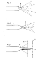
- Figure 2 shows an enlarged view of the nozzle with free jet expansion. Decay of the starting compound is initiated in front of, in or behind the nozzle opening 8, unimolecular decay in single-component systems, higher molecular weight reactions in multi-component systems.
- the disintegration in the flowing gas can be initiated, for example, by plasma chemistry by glow discharges, HF / RF discharges, thermal arc plasmas or thermally by means of resistance or induction heating, photochemically by means of CO2 or excimer lasers or by means of a spark gap.
- SiH4 breaks down into SiH2, SiH, Si, Si2 and H, with parts also being retained as SiH4.
- the ent standing hydrogen-containing condensable molecules cause a relative vapor supersaturation, which leads to gas phase cluster formation.
- Microclusters are associations of a few tens to a hundred atoms or molecules. The cluster formation takes place in a period of about 10 ⁇ 6 seconds after decay.
- the mean gas kinetic velocity is proportional to the root of the reciprocal mass
- the relative mass of the hydrogen molecules (approx.
- Figure 3 shows a nozzle with controlled nozzle expansion.
- the rate of expansion can be controlled via the opening angle ⁇ , the Mach number M is proportional to the opening angle ⁇ (M ⁇ ).
- M ⁇ the opening angle
- Figure 4 shows the expansion of the particles into a vacuum.
- the clusters do not attach themselves to the expanding flow, but remain in the center of the flow 14 due to their excess translation. Due to their high relative mass, the clusters cannot be easily dislodged.
- the target 12 to be coated is arranged in the expansion beam.
- the target 12 does not have to be heated, but in the case of heating, the layer formation can also be influenced by the change in temperature.
- the clusters pass through the shock wave and are heated up after they have cooled down on the way between cluster formation and shock wave, so that they reach approximately the same temperature as before the nozzle passage. Then the clusters hit the target with a large excess of impulses and burst there into an amorphous, very adherent layer (impulse-impact effect). Care must be taken to ensure that not too much material strikes so that controlled layers are created and no powder.
- the application of material can be influenced by changing the flow velocity, the concentration of the initial mixture, the plasma energy and the vacuum pump output.
- the process described can be used to produce layers with excellent mechanical adhesion to the substrate.
- the targeted application of the decay products enables a high material yield.
- the deposition rate is increased from 1 ⁇ m / h to over 10 ⁇ m / h.
- field effect transistors FET
- FET field effect transistors
- slot nozzles possibly several nozzles operated in parallel, and substrate moved uniformly in front of the nozzle, a practically unlimited surface extension of the layers can be achieved.
- a Another important factor is the cost reduction associated with the invention. The lower material requirements and the shorter production times bring significant savings.
- a switching ratio improvement by a factor of 10 is achieved compared to conventional methods.
- the method can also be used to produce metal-ceramic layers and glasses.
- layers can be produced from materials of which gaseous compounds exist or sufficient concentrations can be produced from solid or liquid compounds by sublimation or evaporation processes.
- the possibility of the multi-element composition of the layers, which can be controlled via the gas phase, makes it possible to produce 3/5 compound semiconductors and n- or p-doped semiconductor layers directly and in succession.
- the process is also suitable for the production of multi-component magnetic materials and amorphous metal layers.
- a flow reactor is described with a diameter of 1 cm and an extended nozzle with a Hole diameter of 0.8 mm. Platinum electrodes are melted into the flow reactor to produce a glow plasma.
- a mixture of 99 vol.% He and 1 vol.% SiH4 is used as the gas mixture.
- the working pressure in the plasma reactor is 10 torr with a stationary glow discharge and the plasma voltage is 2000 V with a plasma current of 5 mA.
- the suction pressure of the pumps is 10 Expansion2 Torr on the expansion side.
- a microscope carrier glass plate is used as the substrate target, which, apart from cleaning the surface with methanol, is not subjected to any further treatment.
- a layer of amorphous, hydrogen-containing silicon is formed with a deposition rate of approx. 0.3 ⁇ m / min.
- a correspondingly prepared circuit board for controlling flat screens by means of ⁇ -Si: H field-effect transistors is used as the substrate target.
- the FETs produced by the process according to the invention are distinguished by a switching ratio that is better by a factor of> 10 compared to conventionally produced FETs.
Landscapes
- Chemical & Material Sciences (AREA)
- General Chemical & Material Sciences (AREA)
- Chemical Kinetics & Catalysis (AREA)
- Engineering & Computer Science (AREA)
- Materials Engineering (AREA)
- Mechanical Engineering (AREA)
- Metallurgy (AREA)
- Organic Chemistry (AREA)
- Physics & Mathematics (AREA)
- Optics & Photonics (AREA)
- Health & Medical Sciences (AREA)
- Toxicology (AREA)
- Physical Deposition Of Substances That Are Components Of Semiconductor Devices (AREA)
- Chemical Vapour Deposition (AREA)
Applications Claiming Priority (2)
| Application Number | Priority Date | Filing Date | Title |
|---|---|---|---|
| DE3628443A DE3628443C1 (de) | 1986-08-21 | 1986-08-21 | Verfahren zur Erzeugung amorpher Schichten |
| DE3628443 | 1986-08-21 |
Publications (3)
| Publication Number | Publication Date |
|---|---|
| EP0257302A2 true EP0257302A2 (fr) | 1988-03-02 |
| EP0257302A3 EP0257302A3 (en) | 1990-08-22 |
| EP0257302B1 EP0257302B1 (fr) | 1993-12-08 |
Family
ID=6307896
Family Applications (1)
| Application Number | Title | Priority Date | Filing Date |
|---|---|---|---|
| EP87110585A Expired - Lifetime EP0257302B1 (fr) | 1986-08-21 | 1987-07-22 | Procédé de fabrication de couches amorphes |
Country Status (3)
| Country | Link |
|---|---|
| US (1) | US4942057A (fr) |
| EP (1) | EP0257302B1 (fr) |
| DE (1) | DE3628443C1 (fr) |
Cited By (1)
| Publication number | Priority date | Publication date | Assignee | Title |
|---|---|---|---|---|
| EP0351905A3 (en) * | 1988-07-16 | 1990-08-22 | Philips Patentverwaltung Gmbh | Solid bodies production process |
Families Citing this family (8)
| Publication number | Priority date | Publication date | Assignee | Title |
|---|---|---|---|---|
| FR2664294B1 (fr) * | 1990-07-06 | 1992-10-23 | Plasmametal | Procede de metallisation d'une surface. |
| US5286331A (en) * | 1991-11-01 | 1994-02-15 | International Business Machines Corporation | Supersonic molecular beam etching of surfaces |
| US5764849A (en) * | 1996-03-27 | 1998-06-09 | Micron Technology, Inc. | Solid precursor injector apparatus and method |
| US6271802B1 (en) * | 1997-04-14 | 2001-08-07 | Mems Optical, Inc. | Three dimensional micromachined electromagnetic device and associated methods |
| US6327221B1 (en) | 1999-09-20 | 2001-12-04 | Honeywell International Inc. | Steered beam ultrasonic sensor for object location and classification |
| US9157152B2 (en) * | 2007-03-29 | 2015-10-13 | Tokyo Electron Limited | Vapor deposition system |
| JP6545053B2 (ja) * | 2015-03-30 | 2019-07-17 | 東京エレクトロン株式会社 | 処理装置および処理方法、ならびにガスクラスター発生装置および発生方法 |
| CN110265709B (zh) * | 2019-06-18 | 2022-07-26 | 济宁克莱泰格新能源科技有限公司 | 表面包覆改性的锂镧锆氧基固体电解质材料及其制备方法和应用 |
Family Cites Families (17)
| Publication number | Priority date | Publication date | Assignee | Title |
|---|---|---|---|---|
| GB1483966A (en) * | 1974-10-23 | 1977-08-24 | Sharp Kk | Vapourized-metal cluster ion source and ionized-cluster beam deposition |
| DE2631881C2 (de) * | 1975-07-18 | 1982-11-25 | Futaba Denshi Kogyo K.K., Mobara, Chiba | Verfahren zur Herstellung eines Halbleiterbauelementes |
| JPS5399762A (en) * | 1977-02-12 | 1978-08-31 | Futaba Denshi Kogyo Kk | Device for producing compound semiconductor film |
| JPS53110973A (en) * | 1977-03-10 | 1978-09-28 | Futaba Denshi Kogyo Kk | Method and apparatus for manufacturing compounds |
| US4328257A (en) * | 1979-11-26 | 1982-05-04 | Electro-Plasma, Inc. | System and method for plasma coating |
| JPS58167602A (ja) * | 1982-03-29 | 1983-10-03 | Futaba Corp | 有機物薄膜の形成方法 |
| US4521447A (en) * | 1982-10-18 | 1985-06-04 | Sovonics Solar Systems | Method and apparatus for making layered amorphous semiconductor alloys using microwave energy |
| JPS59156996A (ja) * | 1983-02-23 | 1984-09-06 | Koito Mfg Co Ltd | 化合物結晶膜の製造方法とその装置 |
| JPS59207631A (ja) * | 1983-05-11 | 1984-11-24 | Semiconductor Res Found | 光化学を用いたドライプロセス装置 |
| US4582731A (en) * | 1983-09-01 | 1986-04-15 | Battelle Memorial Institute | Supercritical fluid molecular spray film deposition and powder formation |
| WO1987002026A1 (fr) * | 1984-05-28 | 1987-04-09 | Shuhara Akira | Procede de production d'un film a base de bioxyde de silicium |
| US4559096A (en) * | 1984-06-25 | 1985-12-17 | The United States Of America As Represented By The United States Department Of Energy | Method of precisely modifying predetermined surface layers of a workpiece by cluster ion impact therewith |
| JPS6353259A (ja) * | 1986-08-22 | 1988-03-07 | Mitsubishi Electric Corp | 薄膜形成方法 |
| US4740267A (en) * | 1987-02-20 | 1988-04-26 | Hughes Aircraft Company | Energy intensive surface reactions using a cluster beam |
| US4856457A (en) * | 1987-02-20 | 1989-08-15 | Hughes Aircraft Company | Cluster source for nonvolatile species, having independent temperature control |
| JPS63270458A (ja) * | 1987-04-27 | 1988-11-08 | Mitsubishi Electric Corp | 化合物薄膜形成装置 |
| JP2501828B2 (ja) * | 1987-06-09 | 1996-05-29 | 三菱電機株式会社 | 薄膜蒸着装置 |
-
1986
- 1986-08-21 DE DE3628443A patent/DE3628443C1/de not_active Expired
-
1987
- 1987-07-22 EP EP87110585A patent/EP0257302B1/fr not_active Expired - Lifetime
- 1987-08-14 US US07/085,854 patent/US4942057A/en not_active Expired - Fee Related
Cited By (1)
| Publication number | Priority date | Publication date | Assignee | Title |
|---|---|---|---|---|
| EP0351905A3 (en) * | 1988-07-16 | 1990-08-22 | Philips Patentverwaltung Gmbh | Solid bodies production process |
Also Published As
| Publication number | Publication date |
|---|---|
| US4942057A (en) | 1990-07-17 |
| EP0257302B1 (fr) | 1993-12-08 |
| DE3628443C1 (de) | 1988-02-11 |
| EP0257302A3 (en) | 1990-08-22 |
Similar Documents
| Publication | Publication Date | Title |
|---|---|---|
| DE3884653T2 (de) | Verfahren und Vorrichtung zur Gasphasenabscheidung von Diamant. | |
| DE69125118T2 (de) | Verfahren zur Herstellung eines Diamant-Überzuges | |
| EP0523314B1 (fr) | Appareil pour l'évaporation d'un liquide | |
| DE69522115T2 (de) | Verfahren zur herstellung einer hartstoffschutzschicht | |
| EP0625218B1 (fr) | Procede et dispositif de modification de surfaces par reactions physico-chimiques de gaz ou de vapeurs sur les surfaces a l'aide d'ions fortement charges | |
| DE69605280T2 (de) | Verfahren zum aufbringen diamantähnlicher kohlenstoff-filme | |
| EP0478909B1 (fr) | Procédé et appareillage pour la fabrication d'une couche de diamant | |
| DE69815348T2 (de) | Vorrichtung und verfahren zur keimbildung und abscheidung von diamant mittels heissdraht-dc-plasma | |
| DE69516053T2 (de) | Erzeugung eines Diamantfilmes | |
| EP0663023B1 (fr) | Diamant depose par heteroepitaxie | |
| DE3810237C2 (fr) | ||
| EP0257302B1 (fr) | Procédé de fabrication de couches amorphes | |
| EP0681314B1 (fr) | Structure composite pour dispositif électronique et procédé de fabrication | |
| EP2718481A1 (fr) | Procédé d'enlèvement de couches de carbone dures | |
| EP2077344A1 (fr) | Procédé destiné au dépot d'une couche de diamant sur un substrat de graphite | |
| DE19958474A1 (de) | Verfahren zur Erzeugung von Funktionsschichten mit einer Plasmastrahlquelle | |
| EP0362275B1 (fr) | Fabrication d'un materiau de base pour semiconducteurs | |
| EP3071725B1 (fr) | Procédé de production d'un corps composite comportant au moins une couche fonctionnelle ou de production ultérieure d'un composant électronique ou optoélectronique | |
| DE3112604C2 (de) | Verfahren zur Herstellung eines amorphen Siliciumfilmes | |
| DE3702242A1 (de) | Verfahren zur herstellung haftfester ic-schichten | |
| DE102017205417A1 (de) | Verfahren zur Ausbildung einer mit poly- oder einkristallinem Diamant gebildeten Schicht | |
| DE3334830A1 (de) | Verfahren zur herstellung eines verbindungshalbleiterfilms | |
| DE3212653A1 (de) | Verfahren zur herstellung von ultrareinen ueberzuegen | |
| DD142568A1 (de) | EINRICHTUNG ZUM REAKTIVEN BESCHICHTEN MIT DEM PLASM&TRON | |
| DE102008028990A1 (de) | Erhöhung der Hochtemperaturoxidationsbeständigkeit von TiAl-Legierungen und daraus bestehenden Bauteilen durch Pl3 |
Legal Events
| Date | Code | Title | Description |
|---|---|---|---|
| PUAI | Public reference made under article 153(3) epc to a published international application that has entered the european phase |
Free format text: ORIGINAL CODE: 0009012 |
|
| AK | Designated contracting states |
Kind code of ref document: A2 Designated state(s): FR GB |
|
| RAP1 | Party data changed (applicant data changed or rights of an application transferred) |
Owner name: DORNIER GMBH |
|
| PUAL | Search report despatched |
Free format text: ORIGINAL CODE: 0009013 |
|
| AK | Designated contracting states |
Kind code of ref document: A3 Designated state(s): FR GB |
|
| 17P | Request for examination filed |
Effective date: 19901031 |
|
| 17Q | First examination report despatched |
Effective date: 19920313 |
|
| GRAA | (expected) grant |
Free format text: ORIGINAL CODE: 0009210 |
|
| AK | Designated contracting states |
Kind code of ref document: B1 Designated state(s): FR GB |
|
| GBT | Gb: translation of ep patent filed (gb section 77(6)(a)/1977) |
Effective date: 19940217 |
|
| ET | Fr: translation filed | ||
| PG25 | Lapsed in a contracting state [announced via postgrant information from national office to epo] |
Ref country code: GB Effective date: 19940722 |
|
| PLBE | No opposition filed within time limit |
Free format text: ORIGINAL CODE: 0009261 |
|
| STAA | Information on the status of an ep patent application or granted ep patent |
Free format text: STATUS: NO OPPOSITION FILED WITHIN TIME LIMIT |
|
| 26N | No opposition filed | ||
| GBPC | Gb: european patent ceased through non-payment of renewal fee |
Effective date: 19940722 |
|
| PG25 | Lapsed in a contracting state [announced via postgrant information from national office to epo] |
Ref country code: FR Effective date: 19950331 |
|
| REG | Reference to a national code |
Ref country code: FR Ref legal event code: ST |