EP0257324A2 - Verfahren und Gerät zum Verarbeiten aufgezeichneter, wellenförmiger Signale - Google Patents
Verfahren und Gerät zum Verarbeiten aufgezeichneter, wellenförmiger Signale Download PDFInfo
- Publication number
- EP0257324A2 EP0257324A2 EP87110935A EP87110935A EP0257324A2 EP 0257324 A2 EP0257324 A2 EP 0257324A2 EP 87110935 A EP87110935 A EP 87110935A EP 87110935 A EP87110935 A EP 87110935A EP 0257324 A2 EP0257324 A2 EP 0257324A2
- Authority
- EP
- European Patent Office
- Prior art keywords
- signal
- waveform
- difference
- memory
- time
- Prior art date
- Legal status (The legal status is an assumption and is not a legal conclusion. Google has not performed a legal analysis and makes no representation as to the accuracy of the status listed.)
- Granted
Links
- 238000000034 method Methods 0.000 title claims description 16
- 238000012545 processing Methods 0.000 title claims description 5
- 230000003252 repetitive effect Effects 0.000 claims abstract description 14
- 230000003111 delayed effect Effects 0.000 claims description 11
- 230000004044 response Effects 0.000 claims description 5
- 238000001914 filtration Methods 0.000 claims 1
- 230000001360 synchronised effect Effects 0.000 abstract description 4
- 238000005070 sampling Methods 0.000 description 11
- 238000012360 testing method Methods 0.000 description 11
- 230000000694 effects Effects 0.000 description 4
- 238000005259 measurement Methods 0.000 description 4
- 239000000047 product Substances 0.000 description 4
- 238000012935 Averaging Methods 0.000 description 2
- 238000009825 accumulation Methods 0.000 description 1
- 230000003044 adaptive effect Effects 0.000 description 1
- 230000008901 benefit Effects 0.000 description 1
- 230000008859 change Effects 0.000 description 1
- 230000001419 dependent effect Effects 0.000 description 1
- 238000010586 diagram Methods 0.000 description 1
- 230000000977 initiatory effect Effects 0.000 description 1
- 230000008569 process Effects 0.000 description 1
- 230000003595 spectral effect Effects 0.000 description 1
- 230000009466 transformation Effects 0.000 description 1
- 238000000844 transformation Methods 0.000 description 1
- 230000001960 triggered effect Effects 0.000 description 1
Images


Classifications
-
- G—PHYSICS
- G01—MEASURING; TESTING
- G01R—MEASURING ELECTRIC VARIABLES; MEASURING MAGNETIC VARIABLES
- G01R13/00—Arrangements for displaying electric variables or waveforms
- G01R13/20—Cathode-ray oscilloscopes
- G01R13/22—Circuits therefor
- G01R13/34—Circuits for representing a single waveform by sampling, e.g. for very high frequencies
- G01R13/345—Circuits for representing a single waveform by sampling, e.g. for very high frequencies for displaying sampled signals by using digital processors by intermediate A.D. and D.A. convertors (control circuits for CRT indicators)
-
- G—PHYSICS
- G01—MEASURING; TESTING
- G01R—MEASURING ELECTRIC VARIABLES; MEASURING MAGNETIC VARIABLES
- G01R13/00—Arrangements for displaying electric variables or waveforms
- G01R13/20—Cathode-ray oscilloscopes
- G01R13/22—Circuits therefor
- G01R13/32—Circuits for displaying non-recurrent functions such as transients; Circuits for triggering; Circuits for synchronisation; Circuits for time-base expansion
Definitions
- This invention relates to a method and apparatus for processing waveform records.
- a number of waveform records representative of respective repetitions of the repetitive signal may be stored, and an averaged waveform may be generated by computing the average of the stored waveform records. If the noise is random, the noise present in the averaged waveform is reduced with respect to the stored waveform records. Therefore, measurements made on the averaged waveform reveal more information about the useful signal than those made on the stored waveform records.
- Waveform records are stored by digitizing the repetitive signal and writing the resulting sequence of N digital words per record into memory.
- a signal is digitized by sampling the signal at a constant clock rate, and quantizing each sample using an analog-to-digital converter.
- waveform records representative of respective repetitions of a repetitive segment of a television signal are stored and averaged, and features of the averaged record are measured, for example in order to determine whether the television signal complies with prescribed standards. Jitter among the records is removed using an algorithm known as ALIGN.
- the ALIGN algorithm is subject to the disadvantage that it does not operate properly if the spectral characteristics of the jitter are not uniform. Also, execution of the ALIGN algorithm is time consuming since it involves three fast-Fourier transformations.
- stored waveform records representative of respective repetitions of a repetitive signal are processed by reading a first waveform record from memory to form a reference signal.
- a second waveform record is read from memory to form a second signal, and the second signal is shifted in time in such a manner as to minimize the power of a difference signal, of which the instantaneous magnitude is representative of the difference in instantaneous magnitude between the reference signal and the time-shifted second signal.
- the waveform records are identical but for jitter, and the power of the difference signal is brought to zero, this implies that the first waveform signal is synchronous with the processed second waveform signal, i.e., there is no jitter between the two signals. If waveform records resulting from the reference signal and the processed second signal are then averaged, the level of noise in the averaged record is reduced relative to the stored records and the averaged record is free of distortion due to jitter.
- a conventional helical scan video tape recorder such as that shown at 2 in FIG. 1, generates a signal in the NTSC format.
- the signal comprises, on each line of the active picture interval, a horizontal sync pulse, color burst and picture information.
- the horizontal sync pulse and the picture information are read from the tape 4 by the VTR, but the color burst is generated in an oscillator 5 by a heterodyne process and is inserted into the signal downstream of the VTR's record/playback heads, with the proper timing relative to the horizontal sync pulse, by a burst inserter 6.
- the output terminal of the VTR is connected to the input terminal 8 of a test and measurement device 10, and a pre-recorded videotape is played on the VTR.
- the tape has the identical test signal recorded on every line. Therefore, the signal received at the terminal 8 is a signal that repeats at line rate, i.e., about 15.75 kHz, and comprises, in each repetition, a horizontal sync pulse, burst and the picture information portion of the test signal.
- the test and measurement device 10 is used to identify and measure distortions in the test signal that might be due to improper operation of the VTR.
- the repetitive signal received at the terminal 8 of the device 10 is digitized by means of an analog-to-digital converter (ADC) 12 that samples the video signal in response to a sampling clock and quantizes the resulting samples and thus generates a stream of digital words.
- ADC analog-to-digital converter
- the sampling clock is generated by a sampling clock generator 14 that is triggered by a horizontal sync separator 16.
- the digital words are written into a random access memory 18 under control of a write address generator 20, which also receives the sampling clock.
- the memory 18 stores a record of n successive repetitions of the test signal that is recorded on the tape 4.
- the sampling clock is generated at four times subcarrier frequency, and therefore each waveform record contains 910 digital words. It will be assumed for the purpose of this description that the test signal includes a portion at subcarrier frequency.
- the waveform (a) illustrates a portion of of the test signal that is at subcarrier frequency and the waveforms (b) and (c) illustrate that same portion of two repetitions and also illustrate the sampling clock times. It will be noted that noise superimposed on the test signal is not shown in FIG. 2.
- the phase of the sampling clock relative to the subcarrier portion of the test signal is subject to change from line to line due to random effects in the sync separator 16, the clock generator 14 and the ADC 12. Accordingly, there is relative jitter between the sampling clock and the successive repetitions of the test signal.
- This jitter is shown in FIG. 2 by the shift ⁇ t in time between the sampling clock times for waveform (c) and those of waveform (b).
- the effect of this jitter is that when the digital words representing the waveforms (b) and (c) are written into memory and are subsequently read from memory, e.g. for averaging, the waveform (c) is shifted in time relative to the waveform (b) (see waveform d).
- the memory portion 18A has 1024 addressable locations, of which only 910 are used to store the reference waveform record ⁇ y1 i ⁇ (In this particular implementation, N is equal to 910.).
- the memory portion 18B is organized as multiple segments each having 1024 addressable locations.
- the ten lower address bits for each of the segments of the memory portion 18B are the same as the address bits for the memory portion 18A. It is therefore possible to read the reference record from the memory portion 18A simultaneously with a selected record in the memory portion 18B. The repetition that is used to form the reference record is selected arbitrarily.
- the reference record ⁇ y1 i ⁇ and a selected record, e.g. ⁇ y2 i ⁇ , are read synchronously from the memory portion 18A and a segment of the memory portion 18B respectively under control of a read address counter 22, driven by a read clock generator 24.
- the digital signals are converted to analog form by a digital-to-analog converter (DAC) 60.
- the resulting analog signals y1 and y2 are applied to an oscilloscope 62.
- the waveforms of the signals generated from the two records are observed, and the waveform y2 is shifted horizontally relative to the waveform y1 in order to achieve coarse coincidence (coincidence to within one clock period) between the two waveforms.
- the amount by which the waveform y2 is shifted is used by a microprocessor 40 to compute an offset that is applied by an offset circuit 64 to the addresses that are applied to the memory segment 18B by the read address counter 22.
- the record ⁇ y2 i ⁇ is repeatedly read from memory using the offset address, and the successive repetitions are applied to an adaptive FIR (finite impulse response) filter 26.
- the filter 26 comprises M delay elements 30, a summation circuit 32, M multipliers 34 connected between the outputs of the delay elements and the summation circuit, and a further multiplier connected between the input of the filter 26 and the summation circuit 32.
- FIG. 1 illustrates M as being equal to four. However, it is preferred that M be rather larger, e.g.
- the delay elements 30 each impose a delay equal to the period of the read clock.
- Each multiplier 34p (where p is an integer from 0 to M) multiplies its digital input word by a factor k p in order to generate an output word that is applied to the summation circuit.
- the values of k p are adjustable in dependence upon control signals received from the processor 40.
- the effect of passing the record ⁇ y2 i ⁇ through the FIR filter is to produce a signal ⁇ y2 i ⁇ of which the waveform in the analog domain is the same as that of the record ⁇ y2 i ⁇ but of which the sampling points have been delayed with respect to those of the record ⁇ y2 i ⁇ .
- the amount of the delay depends on the values of k p .
- the digital signal ⁇ y2 i ⁇ generated by the FIR filter 26 is applied to one input of a subtraction circuit.
- the reference record ⁇ y1 i ⁇ is read from the memory portion 18A and the resulting reference signal is applied to the other input of the subtraction circuit.
- the addresses that are applied to the memory portion are each one LSB less than those applied to the memory portion 18B, with result that the reference signal is delayed by one clock period. This one LSB offset is imposed by an offset circuit 66 under control of the processor 40.
- the subtraction circuit 42 receives the digital word y2 j ⁇ from the FIR filter, it receives the digital word y1, j-1 from the memory portion 18A and provides an output digital word z j representing the difference between the digital word y1, j-1 of the reference record and the corresponding digital word y2 j ⁇ of the delayed version of the selected waveform record.
- the digital word z j provided by the subtraction circuit is applied to a squaring circuit 44, to form the word z j 2, and this word is applied to an accumulator 46 which forms the sum of the digital words z j 2 for values of j from M+1 to N.
- the value accumulated by the accumulator is applied to the processor 40.
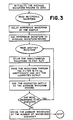
- the processor 40 executes an algorithm to adjust the factors k p following each accumulation in such a manner as to reduce the value stored in the accumulator.
- each corrected record is generated, it is written back into the memory portion 18B in lieu of the uncorrected version of the selected record.
- Each record stored in the memory portion 18B is corrected in this manner and is replaced in the memory portion 18B by its corrected version.
- the corrected records and the reference record are applied to an averager 50 and the resulting averaged waveform record is stored in a waveform memory 52 and is used as the basis for measuring features of the video signal.
- the accumulator 46 store the output of the squaring circuit 42 for every pair of digital words.
- each record contains 910 digital words, good results can be obtained if the sum of the squares of about 500 words is accumulated, and satisfactory results can be obtained if the sum of the squares of at least 100 samples is generated. Since values of y2 i ⁇ are created only for values of i from M + 1 to N, the first M words of the corrected record are lost. However, the disadvantage of losing approximately 1% of the corrected record is outweighed by the advantage of the jitter being removed rapidly and substantially completely.
- the waveform records By use of the apparatus shown in FIG. 1, it is possible to bring the waveform records into near perfect coincidence, i.e., coincidence to within substantially less than one sample interval.
- the reason for delaying the reference signal ⁇ y1 ⁇ by one clock period after coarse coincidence has been achieved, is in order to make certain that fine coincidence can be achieved by only delaying the signal ⁇ y2 ⁇ , so that it is not necessary to include advancing elements in the filter 26.
- the same result may be achieved by adding one LSB to the addresses applied to the memory portion 18B, so as to advance the signal ⁇ y2 ⁇ by one clock period before it is applied to the FIR filter.
- the clock generator is synchronized with reference to the repetitive input signal by triggering the clock generator from the horizontal sync pulse.
- the clock pulses may be synchronized by both triggering the clock generator and initiating generation of the repetitive signal in response to the same event, and in yet other applications, the clock pulses and the repetitive input signal are asynchronous.
Landscapes
- Physics & Mathematics (AREA)
- General Physics & Mathematics (AREA)
- Analogue/Digital Conversion (AREA)
- Television Signal Processing For Recording (AREA)
- Testing, Inspecting, Measuring Of Stereoscopic Televisions And Televisions (AREA)
- Recording Or Reproducing By Magnetic Means (AREA)
- Complex Calculations (AREA)
Applications Claiming Priority (2)
| Application Number | Priority Date | Filing Date | Title |
|---|---|---|---|
| US901668 | 1986-08-29 | ||
| US06/901,668 US4825379A (en) | 1986-08-29 | 1986-08-29 | Method and apparatus for processing waveform records for jitter elimination prior to averaging in determining signal to noise ratio |
Publications (3)
| Publication Number | Publication Date |
|---|---|
| EP0257324A2 true EP0257324A2 (de) | 1988-03-02 |
| EP0257324A3 EP0257324A3 (en) | 1990-05-02 |
| EP0257324B1 EP0257324B1 (de) | 1994-06-08 |
Family
ID=25414613
Family Applications (1)
| Application Number | Title | Priority Date | Filing Date |
|---|---|---|---|
| EP87110935A Expired - Lifetime EP0257324B1 (de) | 1986-08-29 | 1987-07-28 | Verfahren und Gerät zum Verarbeiten aufgezeichneter, wellenförmiger Signale |
Country Status (4)
| Country | Link |
|---|---|
| US (1) | US4825379A (de) |
| EP (1) | EP0257324B1 (de) |
| JP (1) | JPS6364175A (de) |
| DE (1) | DE3750001T2 (de) |
Cited By (5)
| Publication number | Priority date | Publication date | Assignee | Title |
|---|---|---|---|---|
| EP0335496A3 (en) * | 1988-03-21 | 1989-10-18 | Tektronix, Inc. | Waveform timing alignment system for digital oscilloscopes |
| WO1993004563A1 (en) * | 1991-08-21 | 1993-03-04 | British Broadcasting Corporation | Decoding of composite television signals |
| EP0554973A3 (de) * | 1992-01-31 | 1994-01-05 | Tektronix Inc | |
| WO1997014970A1 (en) * | 1995-10-20 | 1997-04-24 | Massachusetts Institute Of Technology | System and method of eliminating systematic noise in stimulus-response systems |
| EP0869368A3 (de) * | 1997-04-04 | 2000-12-20 | Tektronix, Inc. | Verfahren und Vorrichtung zum digitalen Abtasten eines elektrischen Wellenzuges |
Families Citing this family (9)
| Publication number | Priority date | Publication date | Assignee | Title |
|---|---|---|---|---|
| US4890165A (en) * | 1987-04-06 | 1989-12-26 | Canon Kabushiki Kaisha | Image pick-up apparatus for producing video signals of high information density in time base direction |
| US5185874A (en) * | 1989-10-30 | 1993-02-09 | Tektronix, Inc. | Address generator for high speed data averager |
| US5119321A (en) * | 1990-05-14 | 1992-06-02 | Harris Corporation | Adaptive threshold suppression of impulse noise |
| US5121632A (en) * | 1991-01-03 | 1992-06-16 | Magnetrol International, Incorporated | Point level switch |
| US5557196A (en) * | 1993-08-25 | 1996-09-17 | Advantest Corporation | Jitter analyzer |
| US20040151469A1 (en) * | 2003-01-31 | 2004-08-05 | Engholm Kathryn A. | Video editing timeline with measurement results |
| US7136773B2 (en) * | 2003-12-16 | 2006-11-14 | Advantest Corporation | Testing apparatus and testing method |
| US9638673B2 (en) * | 2012-10-18 | 2017-05-02 | Olympus Scientific Solutions Americas Inc. | Ultrasonic testing instrument with dithery pulsing |
| US9632136B2 (en) * | 2013-04-04 | 2017-04-25 | International Business Machines Corporation | Precise estimation of arrival time of switching events close in time and space |
Family Cites Families (11)
| Publication number | Priority date | Publication date | Assignee | Title |
|---|---|---|---|---|
| US3504164A (en) * | 1964-04-10 | 1970-03-31 | Sperry Rand Corp | Data processing system for classifying unknown waveform |
| US3506813A (en) * | 1966-06-13 | 1970-04-14 | Hewlett Packard Co | Signal-to-noise ratio enhancement methods and means |
| US3446949A (en) * | 1966-10-28 | 1969-05-27 | Hewlett Packard Co | Signal-to-noise ratio enhancement methods and means |
| GB1443705A (en) * | 1972-12-15 | 1976-07-21 | Int Research & Dev Co Ltd | Rock drills |
| US4170992A (en) * | 1978-01-05 | 1979-10-16 | Hewlett-Packard Company | Fiducial point location |
| FR2478320A1 (fr) * | 1980-03-17 | 1981-09-18 | Telediffusion Fse | Dispositif d'acquisition et de moyennage des echantillons d'un signal periodique bruite |
| US4455634A (en) * | 1982-01-12 | 1984-06-19 | Discovision Associates | Audio/video quality monitoring system |
| US4540982A (en) * | 1982-05-17 | 1985-09-10 | Tektronix, Inc. | Delay compensation method and apparatus for digital display systems |
| US4555765A (en) * | 1982-09-14 | 1985-11-26 | Analogic Corporation | Multi-mode oscilloscope trigger with compensating trigger delay |
| US4505512A (en) * | 1982-12-06 | 1985-03-19 | Schmeichel Steven C | Roll-up tarp apparatus |
| US4628254A (en) * | 1984-01-16 | 1986-12-09 | Tektronix, Inc. | Method for digitally measuring waveforms |
-
1986
- 1986-08-29 US US06/901,668 patent/US4825379A/en not_active Expired - Fee Related
-
1987
- 1987-07-28 EP EP87110935A patent/EP0257324B1/de not_active Expired - Lifetime
- 1987-07-28 DE DE3750001T patent/DE3750001T2/de not_active Expired - Fee Related
- 1987-08-29 JP JP62216270A patent/JPS6364175A/ja active Pending
Cited By (7)
| Publication number | Priority date | Publication date | Assignee | Title |
|---|---|---|---|---|
| EP0335496A3 (en) * | 1988-03-21 | 1989-10-18 | Tektronix, Inc. | Waveform timing alignment system for digital oscilloscopes |
| WO1993004563A1 (en) * | 1991-08-21 | 1993-03-04 | British Broadcasting Corporation | Decoding of composite television signals |
| EP0554973A3 (de) * | 1992-01-31 | 1994-01-05 | Tektronix Inc | |
| WO1997014970A1 (en) * | 1995-10-20 | 1997-04-24 | Massachusetts Institute Of Technology | System and method of eliminating systematic noise in stimulus-response systems |
| US5640124A (en) * | 1995-10-20 | 1997-06-17 | Massachusetts Institute Of Technology | System and method of eliminating systematic noise in stimulus-response systems |
| EP0869368A3 (de) * | 1997-04-04 | 2000-12-20 | Tektronix, Inc. | Verfahren und Vorrichtung zum digitalen Abtasten eines elektrischen Wellenzuges |
| EP1666892A3 (de) * | 1997-04-04 | 2006-09-06 | Tektronix, Inc. | Verfahren und Vorrichtung zum digitalen Abtasten eines elektrischen Wellenzuges |
Also Published As
| Publication number | Publication date |
|---|---|
| EP0257324B1 (de) | 1994-06-08 |
| DE3750001T2 (de) | 1994-09-15 |
| JPS6364175A (ja) | 1988-03-22 |
| US4825379A (en) | 1989-04-25 |
| DE3750001D1 (de) | 1994-07-14 |
| EP0257324A3 (en) | 1990-05-02 |
Similar Documents
| Publication | Publication Date | Title |
|---|---|---|
| US4825379A (en) | Method and apparatus for processing waveform records for jitter elimination prior to averaging in determining signal to noise ratio | |
| US4063284A (en) | Time base corrector | |
| US4212027A (en) | Time base compensator | |
| US4495586A (en) | Waveform acquisition apparatus and method | |
| US4694468A (en) | Apparatus useful in channel equalization adjustment | |
| US4263593A (en) | Display interpolator employing a transversal filter for a digital oscilloscope | |
| US4402013A (en) | Video signal analyzer | |
| FR2480544A1 (fr) | Circuit pour realiser une interpolation entre des valeurs prises dans deux rangees de donnees | |
| JPS5918666B2 (ja) | デジタルオシロスコ−プのジツタ低減装置 | |
| US4873646A (en) | Digital Correction of linear system distortion | |
| JPH067694B2 (ja) | ビデオカメラの伝達関数決定法 | |
| US7321847B1 (en) | Apparatus and methods for reduction of coherent noise in a digital signal averager | |
| CA2052225C (en) | Circuit for inserting and separating frequency folding information and method for generating thereof | |
| DE69119284T2 (de) | Zeitbasiskorrigierer | |
| JPS60105386A (ja) | 情報信号の時間軸を変更する装置 | |
| EP0114520A2 (de) | Systeme zur Detektion von Markierungssignalen | |
| US7043406B1 (en) | Apparatus and methods for reduction of coherent noise in a digital signal averager | |
| US5640124A (en) | System and method of eliminating systematic noise in stimulus-response systems | |
| JP2785426B2 (ja) | 時間軸補正装置 | |
| CA1110717A (en) | Time-base compensator | |
| CA1104216A (en) | Time-base compensator | |
| EP0487184A2 (de) | Schaltung zum Aufzeichnen und Wiedergeben eines Referenzsignals für eine Zeitbasiskorrektor | |
| EP1497626B1 (de) | Vorrichtungen und verfahren zur verringerung von kohärentem rauschen in einem digitalen signalmittler | |
| JP3641263B2 (ja) | 時間軸誤差検出器及びこれを用いた時間軸誤差補正装置 | |
| SU1727172A1 (ru) | Способ измерени временных искажений видеомагнитофона |
Legal Events
| Date | Code | Title | Description |
|---|---|---|---|
| PUAI | Public reference made under article 153(3) epc to a published international application that has entered the european phase |
Free format text: ORIGINAL CODE: 0009012 |
|
| AK | Designated contracting states |
Kind code of ref document: A2 Designated state(s): DE FR GB NL |
|
| PUAL | Search report despatched |
Free format text: ORIGINAL CODE: 0009013 |
|
| RHK1 | Main classification (correction) |
Ipc: H04N 17/06 |
|
| AK | Designated contracting states |
Kind code of ref document: A3 Designated state(s): DE FR GB NL |
|
| 17P | Request for examination filed |
Effective date: 19900420 |
|
| 17Q | First examination report despatched |
Effective date: 19920514 |
|
| RAP1 | Party data changed (applicant data changed or rights of an application transferred) |
Owner name: TEKTRONIX, INC. |
|
| GRAA | (expected) grant |
Free format text: ORIGINAL CODE: 0009210 |
|
| AK | Designated contracting states |
Kind code of ref document: B1 Designated state(s): DE FR GB NL |
|
| PG25 | Lapsed in a contracting state [announced via postgrant information from national office to epo] |
Ref country code: NL Effective date: 19940608 Ref country code: FR Effective date: 19940608 |
|
| REF | Corresponds to: |
Ref document number: 3750001 Country of ref document: DE Date of ref document: 19940714 |
|
| EN | Fr: translation not filed | ||
| NLV1 | Nl: lapsed or annulled due to failure to fulfill the requirements of art. 29p and 29m of the patents act | ||
| PLBE | No opposition filed within time limit |
Free format text: ORIGINAL CODE: 0009261 |
|
| STAA | Information on the status of an ep patent application or granted ep patent |
Free format text: STATUS: NO OPPOSITION FILED WITHIN TIME LIMIT |
|
| 26N | No opposition filed | ||
| PGFP | Annual fee paid to national office [announced via postgrant information from national office to epo] |
Ref country code: GB Payment date: 20000622 Year of fee payment: 14 |
|
| PGFP | Annual fee paid to national office [announced via postgrant information from national office to epo] |
Ref country code: DE Payment date: 20000629 Year of fee payment: 14 |
|
| PG25 | Lapsed in a contracting state [announced via postgrant information from national office to epo] |
Ref country code: GB Free format text: LAPSE BECAUSE OF NON-PAYMENT OF DUE FEES Effective date: 20010728 |
|
| GBPC | Gb: european patent ceased through non-payment of renewal fee |
Effective date: 20010728 |
|
| PG25 | Lapsed in a contracting state [announced via postgrant information from national office to epo] |
Ref country code: DE Free format text: LAPSE BECAUSE OF NON-PAYMENT OF DUE FEES Effective date: 20020501 |