EP0257528B1 - Photokathoden für Elektronenbildprojektion - Google Patents
Photokathoden für Elektronenbildprojektion Download PDFInfo
- Publication number
- EP0257528B1 EP0257528B1 EP87111980A EP87111980A EP0257528B1 EP 0257528 B1 EP0257528 B1 EP 0257528B1 EP 87111980 A EP87111980 A EP 87111980A EP 87111980 A EP87111980 A EP 87111980A EP 0257528 B1 EP0257528 B1 EP 0257528B1
- Authority
- EP
- European Patent Office
- Prior art keywords
- layer
- photo cathode
- silver
- substrate
- photo
- Prior art date
- Legal status (The legal status is an assumption and is not a legal conclusion. Google has not performed a legal analysis and makes no representation as to the accuracy of the status listed.)
- Expired - Lifetime
Links
Images
Classifications
-
- B—PERFORMING OPERATIONS; TRANSPORTING
- B82—NANOTECHNOLOGY
- B82Y—SPECIFIC USES OR APPLICATIONS OF NANOSTRUCTURES; MEASUREMENT OR ANALYSIS OF NANOSTRUCTURES; MANUFACTURE OR TREATMENT OF NANOSTRUCTURES
- B82Y10/00—Nanotechnology for information processing, storage or transmission, e.g. quantum computing or single electron logic
-
- B—PERFORMING OPERATIONS; TRANSPORTING
- B82—NANOTECHNOLOGY
- B82Y—SPECIFIC USES OR APPLICATIONS OF NANOSTRUCTURES; MEASUREMENT OR ANALYSIS OF NANOSTRUCTURES; MANUFACTURE OR TREATMENT OF NANOSTRUCTURES
- B82Y40/00—Manufacture or treatment of nanostructures
-
- H—ELECTRICITY
- H01—ELECTRIC ELEMENTS
- H01J—ELECTRIC DISCHARGE TUBES OR DISCHARGE LAMPS
- H01J1/00—Details of electrodes, of magnetic control means, of screens, or of the mounting or spacing thereof, common to two or more basic types of discharge tubes or lamps
- H01J1/02—Main electrodes
- H01J1/34—Photo-emissive cathodes
-
- H—ELECTRICITY
- H01—ELECTRIC ELEMENTS
- H01J—ELECTRIC DISCHARGE TUBES OR DISCHARGE LAMPS
- H01J37/00—Discharge tubes with provision for introducing objects or material to be exposed to the discharge, e.g. for the purpose of examination or processing thereof
- H01J37/30—Electron-beam or ion-beam tubes for localised treatment of objects
- H01J37/317—Electron-beam or ion-beam tubes for localised treatment of objects for changing properties of the objects or for applying thin layers thereon, e.g. for ion implantation
- H01J37/3174—Particle-beam lithography, e.g. electron beam lithography
- H01J37/3175—Projection methods, i.e. transfer substantially complete pattern to substrate
-
- H—ELECTRICITY
- H01—ELECTRIC ELEMENTS
- H01J—ELECTRIC DISCHARGE TUBES OR DISCHARGE LAMPS
- H01J9/00—Apparatus or processes specially adapted for the manufacture, installation, removal, maintenance of electric discharge tubes, discharge lamps, or parts thereof; Recovery of material from discharge tubes or lamps
- H01J9/02—Manufacture of electrodes or electrode systems
- H01J9/12—Manufacture of electrodes or electrode systems of photo-emissive cathodes; of secondary-emission electrodes
-
- H—ELECTRICITY
- H01—ELECTRIC ELEMENTS
- H01J—ELECTRIC DISCHARGE TUBES OR DISCHARGE LAMPS
- H01J2201/00—Electrodes common to discharge tubes
- H01J2201/34—Photoemissive electrodes
- H01J2201/342—Cathodes
- H01J2201/3421—Composition of the emitting surface
- H01J2201/3425—Metals, metal alloys
-
- H—ELECTRICITY
- H01—ELECTRIC ELEMENTS
- H01J—ELECTRIC DISCHARGE TUBES OR DISCHARGE LAMPS
- H01J2201/00—Electrodes common to discharge tubes
- H01J2201/34—Photoemissive electrodes
- H01J2201/342—Cathodes
- H01J2201/3421—Composition of the emitting surface
- H01J2201/3426—Alkaline metal compounds, e.g. Na-K-Sb
-
- H—ELECTRICITY
- H01—ELECTRIC ELEMENTS
- H01J—ELECTRIC DISCHARGE TUBES OR DISCHARGE LAMPS
- H01J2237/00—Discharge tubes exposing object to beam, e.g. for analysis treatment, etching, imaging
- H01J2237/30—Electron or ion beam tubes for processing objects
- H01J2237/317—Processing objects on a microscale
- H01J2237/3175—Lithography
- H01J2237/31777—Lithography by projection
- H01J2237/31779—Lithography by projection from patterned photocathode
Definitions
- the present invention relates to photo cathodes used in electron image projection apparatus.
- Photo lithography techniques are important in the production of integrated circuits (ICs).
- ICs integrated circuits
- an electron image projection technique has been proposed, by T. W. O ⁇ Keefe et al in "An Electron Imaging System for the Fabrication of Integrated Circuits", Solid State Electronics, Vol. 12, page 841, 1969, as a technique which might satisfy the demand for sub-micron resolution.
- This technique has been intensively studied and developed by many people, for example as reported by I. Mori et al in "An Electron Beam-Image-Projection System for Submicron", Toshiba Review, Vol. 41, No. 5, 1986.
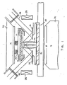
- FIG. 1 The main structure of an electron image projection apparatus in vacuum (1,33.10 -7 to 1,33.10 -4 Pa; 10 -9 to 10 -6 Torr) is schematically illustrated in Fig. 1.
- a semiconductor wafer 31 on which the pattern on the mask substrate 11 is to be copied is placed facing and parallel to the mask substrate 11, approximately 30 mm distant, on a wafer holder 30.
- Ultra violet light 38 of a proper wavelength is irradiated on to the front surface of the mask substrate 11, reflected by reflectors 36 (or is irradiated onto the back surface of the mask substrate when that substrate is of transparent material and when an apparatus is used which is not as shown in the Figure).
- the patterned photo cathode is photo electrically excited and emits photo electrons, which are accelerated by an applied voltage of approximately 80 kV between the mask substrate 11 and the wafer 31. This voltage is applied by supplying -80 kV to the mask substrate 11 and 0 V to the wafer 31.
- a magnetic field is applied perpendicular to the surface of the mask substrate 11 as well as the wafer 31. Emitted and accelerated electrons 39 are thus accurately focused on the surface of the wafer 31 by the applied electric and magnetic fields.
- the magnetic field is applied from magnetic poles 33, 34 and a compensation coil 26, for providing a uniform magnetic field.
- E-beam (electron beam) resist material such as PMMA (polymethyl methacrylate) coated on the semiconductor wafer 31 is thus exposed, by the accelerated and focused electrons, with the pattern of the photo cathode material on the mask substrate 11. This is the principle of electron image projection.
- the first is a type using CsI (caesium iodide) and the second is a type using semiconductor material, such as GaAs (gallium arsenide), having caesium, etc., thereon, as disclosed by Yasuda et al in United States Patent application No. 799 321.
- CsI caesium iodide
- GaAs gallium arsenide
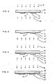
- a photo cathode of the first type for use with back or front illuminating light, is schematically illustrated in Fig. 2.
- a substrate 15 which is made of quartz or sapphire, and is therefore transparent to the illuminating ultra violet light
- a Cr (chrome) layer is patterned as indicated at 12 by a conventional photo mask making technique, such as sputtering, electron beam exposure and etching.
- CsI is deposited over the surface of the patterned substrate 15, as indicated at 10 and 10 ⁇ .
- Ultra violet light 4 is irradiated onto the back surface of the substrate 15 (light 4 ⁇ may alternatively be illuminated on to the front surface), through which the light photo electrically excites the CsI 10 coated directly on the substrate, indicated as photo cathode 14 in Fig. 2.
- the light-excited CsI 10 emits photo electrons, which are pulled out of the surface by the applied electric field.
- the Cr pattern 12 prevents light from reaching CsI layer parts 10 ⁇ formed on that pattern. Thus, the photo cathode 14 is patterned.
- a photo cathode of the second type for use with front illuminating light, is schematically illustrated in Fig. 3.
- a substrate 11 made of a photoelectric material, such as GaAs which is not transparent for the irradiating light
- a tungsten layer for masking non-cathode portions is patterned as indicated at 12 ⁇ by a conventional lithography technique, such as sputtering, electron beam exposure and etching.
- Cs 13 and 13 ⁇ are coated over the surface of the tungsten-patterned GaAs substrate 11.
- Ultra violet light 4 ⁇ is irradiated on to the surface of the patterned substrate 11 having the Cs layering 13 directly thereon.
- Photo cathode portion 14 where the GaAs substrate absorbs the light 4 ⁇ through the Cs layer 13 and produces photo electrons therein, emits electrons, which are pulled out of the surface by the applied electric field.
- the tungsten pattern 12 ⁇ having Cs atoms 13 ⁇ thereon emits a much lesser quantity of photo electrons than the GaAs with Cs thereon. Thus, a patterned photo cathode is formed.
- the surface of the GaAs substrate must be cleaned up by being heated at 630°C or higher in a high vacuum, so that contaminating material on the substrate is evaporated. Accordingly, the atoms of the substrate material can contact Cs atoms for reducing the work function of the surface of the photo cathode.
- this heat cleaning does not always reliably provide a satisfactorily clean surface and less uniform, i.e. less stable, photo electron emissivity may result. Further, the heating process makes masking metal diffuse laterally into the cathode portion 14 which is not masked by the masking metal.
- the borderlines between masked and non-masked areas are made less sharp, namely blurred, by this diffusion.
- photo electron emissivity deteriorates, resulting in deterioration of sharpness, i.e. resolution, of image projection.
- EP-A-0 182 665 discloses the use of Ag2O in a photo cathode.
- US-A-4 005 465 discloses a photocathode with an emitter layer as silver evaporated onto an insulating layer provided on a semiconductor layer and subsequently treated with caesium and oxygen.
- a photo cathode employing silver as photoelectric material, with a layer of alkali or alkali earth metal on the silver, effective to lower the work function of the silver.
- An embodiment of the present invention can provide a photo cathode structure which is more stable, i.e. less susceptible to damage by the atmosphere and easier to handle for efficient electron image projection operations, and of improved uniformity.
- An embodiment of the present invention can provide a photo cathode structure with which sub-micron resolution can be achieved, as required in VLSI (Very Large Scale Integration) fabrication.
- VLSI Very Large Scale Integration
- a photo cathode patterned on a mask substrate is made of an Ag (silver) layer and several atomic layers of alkali metal or alkali earth metal coated on the silver layer.
- the silver layer may be coated over all of a surface of the substrate, then non-cathode portions masked with a pattern of a non-photoelectric material, such as tungsten.
- the silver layer may itself be patterned to the required cathode pattern
- the substrate may itself be of silver, in effect providing the silver layer mentioned above as an integral part of the substrate.
- a mercury lamp providing light of wavelength 365 nm (3650 Angstroms) can be used.
- a photo cathode structure for front (surface) or back illumination is shown in Fig. 4.
- a substrate 15 of transparent material such as quartz or sapphire
- an Ag (silver) layer 16 is coated to a thickness for example in the range 10 Angstroms to 1 ⁇ m, for instance 15 nm (150 Angstroms), by a method such as sputtering, vapour deposition or plating. If the Ag layer is thinner than 1 nm (10 Angstroms), photo electron emissivity is not secured.
- the layer 12 has a thickness for example in the range 10-400nm (100 to 4000 Angstroms), for instance 100 nm (1000 Angstroms), and may be patterned by any suitable lithography technique, such as E-beam lithography.
- the patterned layer 12 masks locally non-cathode portions.
- an alkali metal such as Cs, K (potassium), or Rb (rubidium)
- an alkali earth metal such as Ba (barium) or Ca (calcium
- Layers designated 17, 17 ⁇ will be referred to as Cs (caesium) layers below, by way of example and for brevity, but it is to be understood that such layers may be of any alkali or alkali earth metal.
- the Cs layer 17, 17 ⁇ may be coated, for example, by a caesium ion beam technique, by evaporation of caesium chromate, or by use of a commercially available so-called caesium dispenser. Heating the substrate in caesium vapour is also effective.
- the substrate 15 After coating with the Cs layer 17, 17 ⁇ , the substrate 15 is heated in vacuo at 50 to 200°C for, generally, 1 to 10 minutes. If heating time is too long, there is a deterioration in exposure contrast, and if it is too short its effect is unreliable, in other words electron emissivity may be low.
- the processed substrate 15 with the Cs layer thereon is loaded in electron image projection apparatus, for example as shown in Fig. 1, generally without being exposed to air, for better electron emissivity. If the apparatus is for back irradiation through the transparent substrate 15 on to the back of the Ag layer 16, the magnet pole 33, 34 are removed and replaced by magnet coils (not shown in Fig. 1) in order to clear a path for light.
- the photo electrons are pulled out by the applied electric field to the surface of the Ag layer, where the Cs coating helps the electrons emerge from the cathode because it reduces the work function of the cathode.
- an exposure contrast i.e. ratio of electron current from photo cathode portions to electron current from masked portions, of as high as approximately 20 can be attained.
- the substrate may be of non-transparent material, and too great a thickness of the Ag layer may cause problems.
- the masking metal pattern 12 shields the Ag layer surface from front irradiating light 4 ⁇ , and thus portions of the Ag layer under the masking pattern do not produce photo electrons, unless the masking pattern is too thin. If light passes through the masking pattern, the projected image becomes less sharp. If the masking pattern is too thick, shadowing of to the masking pattern on to the photo cathode (non-masked) portions can result in deterioration of sharpness of the projected image.
- Fig. 5 illustrates the structure of a photo cathode for back irradiation, in accordance with another embodiment of the present invention.
- This structure has a suitable transparent substrate material, e.g. quartz or sapphire, as in the embodiment of Fig. 4.
- a layer 12 ⁇ of non-photoelectric or non-transparent material such as W, Mo, Cr, Pt, Au, Ti, Ta, or the like, is coated and patterned, similarly to the layer 12 in the embodiment of Fig. 4.
- a silver (Ag) layer 20 is formed over the exposed surfaces of the substrate 15 ⁇ and patterned layer parts 12 ⁇ as in the embodiment of Fig. 4.
- a layer 17, 17 ⁇ of an alkali metal such as Cs, K (potassium), or Rb (rubidium), or an alkali earth metal such as Ba (barium) or Ca (calcium) is coated over the surface of the patterned substrate, to a thickness of as much as several atomic layers.
- Layers designated 17, 17 ⁇ are, as mentioned above, referred to as Cs (caesium) layers in this embodiment and embodiments described below, by way of example and for brevity, but it is to be understood that such layers may be of any alkali or alkali earth metal.
- the photo cathode of Fig. 5 is similar to that of Fig. 4, with the order in which the silver layers (16 in Fig. 4 and 20 in Fig. 5) and e.g. tungsten patterns (12 in Fig. 4 and 12 ⁇ in Fig. 5) are applied to the substrate reversed between Fig. 4 and Fig. 5.
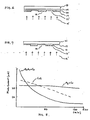
- Fig. 6 illustrates the structure of a photo cathode for front (surface) irradiation, in accordance with another embodiment of the present invention.
- a layer 19 of non-photoelectric material such as W, Mo, Cr, Pt, Au, Ti, Ta, or the like, is coated to a thickness in the range, for example, of 10-400 nm (100 to 4000 Angstroms), for instance 200 nm (2000 Angstroms), by a method such as sputtering.
- This layer acts as a conductor to supply electrons to the photo cathode.
- an Ag layer 20 is patterned.
- the layer 19 has a thickness, for example, in the range 500 Angstroms to 1 ⁇ m, for instance 100 nm (1000 Angstroms).
- the patterning can be accomplished by a method using a lithography technique or a lift-off method.
- the patterned Ag layer 20 thus forms the pattern of the photocathode.
- the thickness of the Ag layer is not critical for the quality of the produced image.
- Cs 17, 17 ⁇ is deposited on all of the exposed surface of the layers 19 and 20, to a thickness of as much as several atomic layers, in the same way as described for Fig. 4.
- the resulting photo cathode is indicated at 14.
- the processed substrate with the Cs layering is loaded in to electron image projection apparatus, for example as shown in Fig. 1, usually without being exposed to air.
- electron image projection apparatus for example as shown in Fig. 1, usually without being exposed to air.
- the patterned Ag layer 20 with Cs layer 17 thereon acts as photo cathode 14 to emit electrons.
- Fig. 7 illustrates the structure of another photo cathode for front (surface) irradiation, in accordance with an embodiment of the present invention.
- a substrate 21 made of Ag is employed in place of a substrate with an Ag layer thereon (see e.g. Fig. 4).
- Other features of the structure of Fig. 7 are similar to those of Fig. 4.
- the structure of Fig. 7 can be used only with front (surface or outer) irradiation.
- a photocathode for electron image projection apparatus, uses silver as a photo electric material, for example in a layer on a substrate, with a layer of alkali or alkali earth metal, such as caesium, on the silver.
- the caesium layer is as thick as several atomic layers and serves to reduce the work function of the photo cathode.
- non-cathode portions On a silver substrate, or a silver layer coated over the whole of a non-silver substrate, non-cathode portions may be masked by a non-photoelectric metal or a non-transparent metal, such as platinum.
- a silver layer may be patterned on a layer of non-photoelectric metal coated on a substrate.
- Light for exciting a photocathode may be irradiated on to the front of the photocathode or onto the back, to reach a silver layer through a transparent substrate, when the photo cathode structure is suitable.
- the alkali/alkali earth metal e.g. caesium
- heating at 50 to 200°C in vacuum is carried out.
- a contrast ratio, ratio of electron currents from cathode and non-cathode portions, as high as 20 can be achieved.
- the low heating temperature prevents lateral diffusion of masking metal, giving sharp edges to the cathode pattern.
- the silver with alkali/alkali earth metal, e.g. caesium, thereon is not susceptible to damage by air, so long life and easy handling can be provided for efficient photolithography processing.
- the low absorption edge of the silver allows the use of a high pressure mercury lamp whose light can easily be focused by a lens.
Landscapes
- Engineering & Computer Science (AREA)
- Chemical & Material Sciences (AREA)
- Nanotechnology (AREA)
- Manufacturing & Machinery (AREA)
- Physics & Mathematics (AREA)
- Crystallography & Structural Chemistry (AREA)
- Theoretical Computer Science (AREA)
- Mathematical Physics (AREA)
- Analytical Chemistry (AREA)
- Condensed Matter Physics & Semiconductors (AREA)
- General Physics & Mathematics (AREA)
- Electron Beam Exposure (AREA)
- Common Detailed Techniques For Electron Tubes Or Discharge Tubes (AREA)
- Preparing Plates And Mask In Photomechanical Process (AREA)
Claims (20)
Applications Claiming Priority (2)
| Application Number | Priority Date | Filing Date | Title |
|---|---|---|---|
| JP192448/86 | 1986-08-18 | ||
| JP61192448A JPS6347928A (ja) | 1986-08-18 | 1986-08-18 | 光電子転写用マスク |
Publications (2)
| Publication Number | Publication Date |
|---|---|
| EP0257528A1 EP0257528A1 (de) | 1988-03-02 |
| EP0257528B1 true EP0257528B1 (de) | 1991-01-30 |
Family
ID=16291471
Family Applications (1)
| Application Number | Title | Priority Date | Filing Date |
|---|---|---|---|
| EP87111980A Expired - Lifetime EP0257528B1 (de) | 1986-08-18 | 1987-08-18 | Photokathoden für Elektronenbildprojektion |
Country Status (5)
| Country | Link |
|---|---|
| US (1) | US5118952A (de) |
| EP (1) | EP0257528B1 (de) |
| JP (1) | JPS6347928A (de) |
| KR (1) | KR910003579B1 (de) |
| DE (1) | DE3767811D1 (de) |
Families Citing this family (8)
| Publication number | Priority date | Publication date | Assignee | Title |
|---|---|---|---|---|
| US5336902A (en) * | 1992-10-05 | 1994-08-09 | Hamamatsu Photonics K.K. | Semiconductor photo-electron-emitting device |
| JP2719297B2 (ja) * | 1993-06-22 | 1998-02-25 | 浜松ホトニクス株式会社 | 透過型光電面および光電管と透過型光電面の製造方法 |
| US6774990B2 (en) * | 2002-08-23 | 2004-08-10 | Intel Corporation | Method to inspect patterns with high resolution photoemission |
| ITMI20070301A1 (it) * | 2007-02-16 | 2008-08-17 | Getters Spa | Supporti comprendenti materiali getter e sorgenti di metalli alcalini o alcalino-terrosi per sistemi di termoregolazione basati su effetto tunnel |
| US8970509B2 (en) * | 2009-12-09 | 2015-03-03 | Lg Display Co., Ltd. | Touch panel and liquid crystal display device including the same |
| EP4002418A1 (de) * | 2020-11-12 | 2022-05-25 | Hamamatsu Photonics K.K. | Metaflächenelement, elektronenröhre und verfahren zur herstellung einer elektronenröhre |
| CN112925171A (zh) * | 2021-01-20 | 2021-06-08 | 桂林理工大学 | 基于阳极氧化铝模板的图案化电子光源及其制造方法 |
| CN112921380B (zh) * | 2021-01-20 | 2022-04-22 | 桂林理工大学 | 基于阳极氧化铝模板的图案化电子光源器件及其制造方法 |
Family Cites Families (16)
| Publication number | Priority date | Publication date | Assignee | Title |
|---|---|---|---|---|
| US1901577A (en) * | 1928-01-04 | 1933-03-14 | Gen Electric | Photo-electric tube |
| DE864585C (de) * | 1936-07-04 | 1953-01-26 | Zeiss Ikon Ag | Photo- oder sekundaeremissionsempfindliche Elektroden |
| GB502024A (en) * | 1936-09-10 | 1939-03-09 | Walter Heimann | Improvements in or relating to mosaic electrodes for electronic scanning devices |
| US2175888A (en) * | 1936-12-31 | 1939-10-10 | Rca Corp | Photoelectric cathode |
| US2439647A (en) * | 1945-07-21 | 1948-04-13 | Philco Corp | Photoelectric tube and method of manufacturing same |
| US2538588A (en) * | 1948-06-23 | 1951-01-16 | Continental Electric Company | Photocell |
| US3672987A (en) * | 1969-12-23 | 1972-06-27 | Westinghouse Electric Corp | Masked photocathode and method of making same |
| US3832560A (en) * | 1973-06-13 | 1974-08-27 | Westinghouse Electric Corp | Method and apparatus for electron beam alignment with a member by detecting cathodoluminescence from oxide layers |
| US4005465A (en) * | 1974-06-04 | 1977-01-25 | The United States Of America As Represented By The Secretary Of The Army | Tunnel emitter photocathode |
| US3960620A (en) * | 1975-04-21 | 1976-06-01 | Rca Corporation | Method of making a transmission mode semiconductor photocathode |
| JPS52122463A (en) * | 1976-04-05 | 1977-10-14 | Rca Corp | Electron emitting electrode |
| GB1589925A (en) * | 1977-11-14 | 1981-05-20 | English Electric Valve Co Ltd | Photoemissive cathodes |
| GB2111299B (en) * | 1981-11-30 | 1986-07-09 | Thermo Electron Corp | High current density photoelectron generators |
| JPS61129826A (ja) * | 1984-11-29 | 1986-06-17 | Fujitsu Ltd | 光電子像の転写方法 |
| JPS61123135A (ja) * | 1984-11-20 | 1986-06-11 | Fujitsu Ltd | 光電子像転写方法 |
| KR910000756B1 (en) * | 1984-11-20 | 1991-02-06 | Fujitsu Ltd | Method for projection photoelectron image |
-
1986
- 1986-08-18 JP JP61192448A patent/JPS6347928A/ja active Pending
-
1987
- 1987-08-17 KR KR1019870008973A patent/KR910003579B1/ko not_active Expired
- 1987-08-18 EP EP87111980A patent/EP0257528B1/de not_active Expired - Lifetime
- 1987-08-18 DE DE8787111980T patent/DE3767811D1/de not_active Expired - Lifetime
-
1990
- 1990-10-24 US US07/605,008 patent/US5118952A/en not_active Expired - Fee Related
Also Published As
| Publication number | Publication date |
|---|---|
| DE3767811D1 (de) | 1991-03-07 |
| KR910003579B1 (ko) | 1991-06-05 |
| US5118952A (en) | 1992-06-02 |
| EP0257528A1 (de) | 1988-03-02 |
| KR880003405A (ko) | 1988-05-17 |
| JPS6347928A (ja) | 1988-02-29 |
Similar Documents
| Publication | Publication Date | Title |
|---|---|---|
| US5395738A (en) | Electron lithography using a photocathode | |
| KR920005634B1 (ko) | 광전자 마스크 및 그것을 사용한 광전자 전사노광방법 | |
| US6723475B2 (en) | Reflection-type mask for use in pattern exposure, manufacturing method therefor, exposure apparatus, and method of manufacturing a device | |
| EP0257528A1 (de) | Photokathoden für Elektronenbildprojektion | |
| EP0182665B1 (de) | Verfahren zum Projizieren eines photoelektrischen Bildes | |
| GB2111299A (en) | High current density photoelectron generators | |
| Saville et al. | Feasibility study of photocathode electron projection lithography | |
| KR20020026532A (ko) | 전자 빔 소스용의 패터닝된 열전도 포토캐소드 | |
| US4968894A (en) | Electrical field enhanced electron image projector | |
| JPS63100729A (ja) | 光電子転写用マスクとその製造方法 | |
| Poppeller et al. | Hot Electron Emission Lithography: a method for efficient large area e-beam projection | |
| KR930001433B1 (ko) | 이온 빔 총 | |
| JPS6066429A (ja) | 光電子像縮小投影式電子ビ−ム露光方法 | |
| JPS635561A (ja) | 光電子ビ−ム転写方法 | |
| Bril et al. | High resolution bubble patterns obtained by electron image projection | |
| JPS6292444A (ja) | 光電子像転写方法 | |
| JPS61289628A (ja) | 光電子像転写方法 | |
| JPS63155726A (ja) | 光電子転写用マスクおよびその製造方法 | |
| JPS60106131A (ja) | 電子ビ−ム露光方法 | |
| JPS62145816A (ja) | 光電子像転写装置 | |
| Stewart et al. | Issues in the repair of x-ray masks | |
| JPS61216323A (ja) | 電子像転写方法 | |
| Karain | The manufacture and characterization of arrays of atomically sharp silicon tips, and their use as photocathodes and electron sources for x-ray generation | |
| JPH01106429A (ja) | 光電子転写装置 | |
| JPH01168024A (ja) | 光電子転写用マスクおよびその製造方法 |
Legal Events
| Date | Code | Title | Description |
|---|---|---|---|
| PUAI | Public reference made under article 153(3) epc to a published international application that has entered the european phase |
Free format text: ORIGINAL CODE: 0009012 |
|
| AK | Designated contracting states |
Kind code of ref document: A1 Designated state(s): DE FR GB |
|
| 17P | Request for examination filed |
Effective date: 19880324 |
|
| 17Q | First examination report despatched |
Effective date: 19890524 |
|
| GRAA | (expected) grant |
Free format text: ORIGINAL CODE: 0009210 |
|
| AK | Designated contracting states |
Kind code of ref document: B1 Designated state(s): DE FR GB |
|
| REF | Corresponds to: |
Ref document number: 3767811 Country of ref document: DE Date of ref document: 19910307 |
|
| ET | Fr: translation filed | ||
| PLBE | No opposition filed within time limit |
Free format text: ORIGINAL CODE: 0009261 |
|
| STAA | Information on the status of an ep patent application or granted ep patent |
Free format text: STATUS: NO OPPOSITION FILED WITHIN TIME LIMIT |
|
| 26N | No opposition filed | ||
| PGFP | Annual fee paid to national office [announced via postgrant information from national office to epo] |
Ref country code: FR Payment date: 19930827 Year of fee payment: 7 |
|
| PGFP | Annual fee paid to national office [announced via postgrant information from national office to epo] |
Ref country code: DE Payment date: 19931030 Year of fee payment: 7 |
|
| PGFP | Annual fee paid to national office [announced via postgrant information from national office to epo] |
Ref country code: GB Payment date: 19940809 Year of fee payment: 8 |
|
| PG25 | Lapsed in a contracting state [announced via postgrant information from national office to epo] |
Ref country code: FR Effective date: 19950428 |
|
| PG25 | Lapsed in a contracting state [announced via postgrant information from national office to epo] |
Ref country code: DE Effective date: 19950503 |
|
| REG | Reference to a national code |
Ref country code: FR Ref legal event code: ST |
|
| PG25 | Lapsed in a contracting state [announced via postgrant information from national office to epo] |
Ref country code: GB Effective date: 19950818 |
|
| GBPC | Gb: european patent ceased through non-payment of renewal fee |
Effective date: 19950818 |