EP0258062A2 - Tampon de données numériques et registre de décalage variable - Google Patents
Tampon de données numériques et registre de décalage variable Download PDFInfo
- Publication number
- EP0258062A2 EP0258062A2 EP87307620A EP87307620A EP0258062A2 EP 0258062 A2 EP0258062 A2 EP 0258062A2 EP 87307620 A EP87307620 A EP 87307620A EP 87307620 A EP87307620 A EP 87307620A EP 0258062 A2 EP0258062 A2 EP 0258062A2
- Authority
- EP
- European Patent Office
- Prior art keywords
- data
- output
- input
- clock
- bus
- Prior art date
- Legal status (The legal status is an assumption and is not a legal conclusion. Google has not performed a legal analysis and makes no representation as to the accuracy of the status listed.)
- Withdrawn
Links
Images




Classifications
-
- G—PHYSICS
- G06—COMPUTING OR CALCULATING; COUNTING
- G06F—ELECTRIC DIGITAL DATA PROCESSING
- G06F5/00—Methods or arrangements for data conversion without changing the order or content of the data handled
- G06F5/06—Methods or arrangements for data conversion without changing the order or content of the data handled for changing the speed of data flow, i.e. speed regularising or timing, e.g. delay lines, FIFO buffers; over- or underrun control therefor
- G06F5/065—Partitioned buffers, e.g. allowing multiple independent queues, bidirectional FIFO's
Definitions
- the invention relates to buffer memories for digital data storage systems, and in particular to data buffers for synchronizing, queuing, and delaying a high speed, asynchronous data and control signal input, such as from the analog to digital converter and timebase circuits of a digital oscilloscope.
- Other applications include magnetic media interfaces and video digital timebase correctors.
- Digital oscilloscopes acquire and store digital data sampled from analog inputs. High sampling rates are used to gather as much information as possible about transient waveforms, resulting in the generation of huge amounts of data.
- Various techniques are used to alter the data flow into the digital data memory to maximize the utilization of the finite amount of available storage. These techniques increase the apparent size of the memory without losing any significant information. Examples include variable timebase rates, sampling only during specified trigger conditions, burst sampling, and adaptive sampling rate (based on evaluating the spectral content of the input signal in real time). These methods produce a variable rate of input data requiring a buffer to smooth the flow of data.
- DRAMs dynamic-type memories
- control circuits There is usually an unavoidable delay in the control circuits, especially spectrum estimator circuits for adaptive sample rate controllers.
- spectrum estimator circuits for adaptive sample rate controllers.
- output synchronization may be necessary to deal with an external storage device.
- the invention provides data buffering apparatus for converting an input digital data stream synchronized with an external input clock to an output digital data stream synchronized with an external output clock from a downstream device, comprising: means for producing an internal clock signal with a frequency at least as high as the external clock frequencies; an internal data bus: an input synchronizer (11) for receiving the input data stream (n) and producing an output data stream on the internal data bus synchronized to the internal clock signal; a first FIFO memory (13) connected to the internal data bus for receiving a first portion (m) of the input data stream and temporarily holding the data until the downstream device is ready to receive the data; a second FIFO memory (15) connected to the internal data bus for receiving a second portion (S) of the input data stream, reading data and writing data coincidentally with the first FIFO memory, and temporarily a programmable number of data words, so that the second portion of the data stream is delayed with respect to the first portion of the data stream; and an output synchronizer (17) connected to the internal data bus for receiving the data
- a three stage system synchronizes the incoming data stream with the memory input clock, buffers the incoming data stream and provides a variable delay for the data.
- the digital data stream from an input device is received by an input synchronizer having its input clocked at the clock rate of the input device clock and its output clocked at a higher internal clock rate.
- the data is written into two FIFO buffers, a master and a slave.
- the master buffer controls the read and write addresses of both buffers, so that the write address of the buffers advances only when valid data is written into the buffers, and the read address advances only when data is read out of the buffers.
- the slave buffer can be programmed with an offset in its read address, so it operates as a delay buffer.
- the data is read out of the buffers into an output synchronizer, having its input clocked at the internal clock rate its output clocked at the clock rate of the memory control.
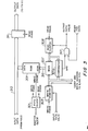
- Figure 1 shows an overall block diagram of a FIFO buffer and delay register constructed in accordance with the preferred embodiment of the invention.
- Data consisting of n-bit wide words is clocked into the input synchronizer 11 by an input clock which is supplied by the same device that is supplying the input data.
- the data supplying device could be, for example, the ADC sampler of a waveform recorder.
- the input synchronizer also provides a "data valid" signal, indicating that new data appears on its output bus. This signal is also synchronous with the internal clock.
- the n-bit data stream is split into two data paths of width m bits and s bits.
- the m bits of data typically control information, go to the master FIFO (with a buffering capacity of f words) and are passed along to the output synchronizer 17 as soon as the output synchronizer is ready to use them.
- the m bits that pass through the master FIFO are buffered but not delayed.
- the slave FIFO 15 operates under the control of the master FIFO 13 to buffer the s-bit data stream, and to delay the s-bit stream by effectively passing the data through a shift register of arbitrary length r. Hence, at least r words, and at most r+f words, are always in the slave FIFO 15.
- the output synchronizer 17 recombines the m-bit and s-bit data streams, and synchronizes the output data to an output clock supplied by the device utilizing the output data.
- the output synchronizer sends back a "ready for data" signal to the master FIFO, indicating that the data receiving device is ready, which is synchronous with the internal clock.
- a internal FIFO clock produces a two phase internal clock signal, write phase and read phase, to control the FIFO RAMs, along with write enable strobes and select inputs for the RAM address multiplexers described below.
- either the input or the output synchronizer will be superfluous because the data will be processed or generated from a system which is also clocked from the internal FIFO clock. Also, it is possible to put a synchronous data processing machine before and/or after the FIFO section and retain both synchronizers.
- the purpose of the data synchronizer is to provide an interface between the data clock from the outside world and the internal memory system clock.
- the internal FIFO clock must run at least as fast as the outside data input clock, but the two will generally not be synchronous. This creates three problems for the input synchronizer.
- the output stage is going to overrun the input stage fairly frequently, i.e., be ready for data when no data is available. Some method of recognizing and reacting to the absence of output data is essential.
- the circuit must be able to simultaneously receive input and send output data. This means there must be storage for two words of data, the one coming in and the one going out.
- the two clocks have a significant chance of becoming coincident, which will cause at least one flip-flop in any implementation to enter a metastable state. This undesirable condition must not be allowed to upset the sequence of operations in the circuit or corrupt the output data.
- Figure 2 shows a more detailed block diagram of the input synchronizer II.
- the input synchronizer consists of two n-bit data registers, 201 and 203, with positive edge-triggered clocks and 3-state outputs with active LOW output-enable control, three D-type positive edge-triggered flip-flops, 205, 207 and 209, two NAND gates, 215 and 217, and an exclusive-OR gate, 219. (In the discussion that follows, the first data word after power up is considered to be number zero and hence is an even-numbered data word.)
- the two data registers are connected in parallel to the incoming data on data bus 21I.
- the input flip-flop 205 has its D input connected to its Q-bar output so that it operates in toggle mode.
- the input flip-flop 205 is clocked by the external data input clock, so during even-numbered input clock periods the input flip-flop 205 is in the low state and during odd-numbered clock periods, it is in the high state.
- Even register 201 is clocked from the Q output of flip-flop 205 and odd register 203 is clocked from the Q-bar output of flip-flop 205.
- even register 201 clocks in even-numbered data words at the end of even numbered clock periods
- odd register 203 clocks in odd-numbered data words.
- the data output ports of registers 201 and 203 are connected on parallel to output data bus 213 to transfer data to the master and slave FIFOs.
- the Q output of flip-flop 205 also drives the D-input of the sync flip-flop 207 which is clocked by the WRITE PHASE from the internal FIFO clock and thus synchronizes changes in the state of the input flip-flop to the internal clock.
- Synch flip-flop 207 inherently has some probability of entering a metastable state when the input and internal clocks are changing state simultaneously. However, it has the entire period of the internal FIFO clock (less set-up time of the next stage and the propagation delay of the gate) to exit the metastable state. Typically, 50 to 200 nsec. need to be provided from this to occur, depending on the logic family and bit error rate tolerance.
- the Q output of synch flip-flop 207 drives the D input of output flip-flop 209 which is also clocked by the WRITE PHASE from the internal FIFO clock.
- the Q outputs of synch flip-flop 207 and output flip-flop 209 are applied to exclusive-OR gate 219.
- the Q and Q-bar outputs of flip-flop 209 are applied respectively to NAND gates 215 and 217, which also receive the WRITE PHASE signal from the internal FIFO clock.
- the output of NAND gate 215 is applied to the output enable terminal of even register 201, and the output of NAND gate 217 is applied to the output enable terminal of odd register 203.
- sync flip-flop 207 detects a change in state of the input flip-flop 205, then on the next internal clock edge the sync flip-flop will be in the state opposite that of the output flip-flop 209.
- the exclusive-OR gate 219 will go high indicating "data valid”.
- the input synchronizer assumes that the FIFO sections clock the data in on this edge.
- the other event which occurs on a data valid edge of the internal FIFO clock is that the output flip-flop will change state, and enable the 3-state output of the opposite register. This acts like a data switch and makes the next word of data available to the FIFOs. Note that this implementation saves an n-bit multiplexer.
- the input flip-flop 205, clocked by the external clock, and the output flip-flop 209, clocked from the internal FIFO clock, are connected thru a synchronizing flip-flop 207 which provides are transition between the two different clocks in the system. This solves the metastable state problem.
- Previous implementations have needed cumbersome and critical timing circuits involving delay lines or one-shot multivibrators to control metastable behavior.
- the exclusive-OR gate 219 generates the "output data valid" signal only when a new data word was clocked into the input synchronizer during the previous internal FIFO clock period.
- the signal "data valid” goes high during the same internal clock period that the data it refers to is valid. This allows the FIFOs to handle the problem of the synchronizer running out of data.
- the master FIFO 13 is used only for the m-bit control signal associated with the data stream. However, it is an integral part of the pipeline FIFO used for the s-bit data stream. This is because it handles the housekeeping details having to do with how full or empty the FIFO buffer is. It also shares part of the write counter 303.
- FIFO First-In-First-Out
- the purpose of the FIFO (First-In-First-Out) buffer is to smooth out variations in the rate at which data is output, for example to a downstream storage memory, and to temporarily hold data if the downstream memory is unable to accept data, for example during memory refresh cycles.
- FIFO 13 can hold up to f+1 words. Data is written in only when the data from input synchronizer 11 is valid and is read out only when the FIFO contains valid data and the output synchronizer 17 is ready to receive data.
- this one is synchronous. Both input and output use the internal FIFO clock, although they run on different phases of it. Data is written into the FIFOs during one phase and read out during the other phase.
- Separate counters, 301 and 305 are used to sequentially address the RAM array 301 for writing and reading data. The counters wrap around when they reach terminal count (modulo f+1) which results in a recirculating memory of f+1 words. As long as the counters never differ by more than f, the "end" of the memory is never reached.
- Figure 3 shows a more detailed block diagram of the master FIFO 13, comprising static RAM array 301 capable of storing f+1 words of m bits each, counters 303 and 305 for read and write addressing, a read/write address multiplexer 307, comparator 309, and output register 311 to store data read out of the FIFO.
- the output register 311 corresponds to the registers of the output synchronizer 17, and is shown separately in Figure 3 to simplify the description of the FIFOs.
- Figure 3 also shows the internal FIFO clock 321.
- the internal FIFO clock 321 produces a two phase internal clock signal.
- the internal clock frequency produces an internal data transfer rate slightly higher than the maximum expected average data input rate.
- Phase 1 of the clock signal, the WRITE PHASE, is applied to the input synchronizer 11, the master FIFO 13 and slave FIFO 15.
- Phase 2 of the clock signal, the READ PHASE is applied to the output synchronizer 17, master FIFO 13 and slave FIFO 15.
- the clock generator produces a WRITE STROBE signal during the phase 1 portion, which is applied to RAM 301 in the master FIFO 13 and to RAM 401 in the slave FIFO 15, and a control signal applied to multiplexer 307 in the master FIFO 13 and to multiplexer 407 in the slave FIFO 15.
- RAM array 301 has a data port with shared input/output pins so that data bus 313 is used to connect together the two input synchronizer registers 201 and 203, the output register 311 and the data pins of RAM 301.
- data bus 313 is used to connect together the two input synchronizer registers 201 and 203, the output register 311 and the data pins of RAM 301.
- the appropriate register in the input synchronizer is enabled to drive bus 313.
- the RAM 301 drives bus 313.
- the read and write addresses for RAM 301 are generated by write counter 303 and read counter 305.
- Multiplexer 307 switches the address bus 315 between the read and write counters depending on the phase of the internal clock.
- the write counter 303 is clocked by the WRITE PHASE signal, but advances only when the data valid signal form the input synchronizer is valid.
- the read counter 305 is clocked by the READ PHASE signal, but advances only when the output data valid signal, described below, is valid.
- the difference between the two counters represents the number of words stored in the FIFO buffer. Hence the read counter is constantly chasing the write counter.
- the outputs of the read and write counters are also applied to comparator 309, which generates a true output only when the counts are not equal, i.e., when the FIFOs are not empty.
- the comparator output and a ready for data signal from the output synchronizer 17 are applied to AND gate 317.
- AND gate 317 produces an output data valid signal which enables the read counter 305 and indicates to the output synchronizer 17 that there is valid data from the FIFOs on bus 313.
- Incoming data is always written into the address that the write counter points to in the RAM address space, even if "data valid" is false.
- the write counter 303 advances to the next memory address only if the input data valid signal is true. Hence, invalid data is overwritten with valid data.
- data is always read out of the RAMs onto bus 313, even if the FIFO is empty.
- the read counter 307 advances to the next memory address and the output synchronizer takes the data only when the output data valid signal is true, indicating that the FIFOs are not empty and the output synchronizer is ready for data.
- the read counter 305 stands still while the new data coming in continues to advance the write counter 303.
- the read counter will start incrementing toward the write counter.
- the data coming into the FIFO will be invalid and the write counter will not advance. This will allow the read counter to move one word closer to the write counter. After enough such events, it will catch up and cause the comparator output to go false.
- the s-bit data stream from the input synchronizer 11 passes thru the slave FIFO 15, which provides a programmable time delay for the data stream.
- the slave FIFO 15 is similar to the master FIFO in configuration and operation, but its address counters 403 and 405 have more bits to control the larger address space (r+f+1) required for the time delayed data stream.
- FIFO 15 is referred to as a slave because the count enable signals from the master FIFO 13 are used to control the address counters of FIFO 15.
- the read counter 405 is preset to a delay value r address counts less than the write counter 303 when the FIFO is initialized. This offset is maintained during subsequent operation, resulting in an r word pipeline delay in the data path.
- the delay r could be set to 2 with respect to the control stream through the master FIFO to allow the trigger circuit two clock periods to recognize a trigger event. Note that the delay is easily programmable to other values.
- FIG. 4 shows a more detailed block diagram of the slave FIFO 15, comprising static RAM array 401 capable of storing f+r+1 words of s bits each, counters 403 and 405 for read and write addressing, a read/write address multiplexer 407 and output register 411 to store data read out of the FIFO.
- the output register 411 corresponds to the registers of the output synchronizer 17, and is shown separately in Figure 4 to simplify the description of the FIFOs.
- RAM array 401 has data port connections like those of RAM 301, so that RAM 401 can read data from the input synchronizer registers and write data to the output register 411 on data bus 413.
- the read and write addresses for RAM 401 are generated by write counter 403 and read counter 405.
- Multiplexer 407 switches the address bus 415 between the read and write counters depending on the phase of the internal clock.
- the write counter 403 is clocked by the WRITE PHASE signal and advances only when the data valid signal from the input synchronizer is valid.
- the read counter 405 is clocked by the READ PHASE signal and advances only when the output data valid signal is valid, thus it is slaved to the buffering control logic of the master FIFO.
- the read counter 405 is initialized at zero minus r by a PIPELINE LENGTH control signal and the write counter is initialized at zero. As long as the counters remain in lockstep, there will be a delay of r words between input and output.
- An alternative arrangement for the address counters is to use the master FIFO write counter 303 for the lower order bits of the slave FIFO write counter 403.
- the two write counters will count in exact synchronization and the lower bits of the two write counters will be identical if the size of the slave counter 403 is an integral multiple of the size of the master counter 303, since they are both initialized to zero.
- the advantage of this arrangement is that hardware can be saved by sharing the counting function for the lower order bits.
- the size of the pipeline will expand and contract at the same rate as the master FIFO buffer expands and contracts.
- the slave FIFO read counter starts out r words behind so that it imparts an r-word delay. Therefore, there will always be r data words in a pipeline that is essentially independent of the variable number of words in the FIFO pipeline.
- the operation of the output synchronizer is similar to the input synchronizer 11 except that the clock control information propagates in the reverse direction, unlike the input synchronizer where the control information and the data flow in the same direction.
- FIG. 5 shows a more detailed block diagram of the output synchronizer 17.
- the output synchronizer consists of two n-bit data registers, 501 and 503, with positive edge-triggered clocks and 3-state outputs with active LOW output-enable control, three D-type positive edge-triggered flip-flops, 505, 507 and 509, and an exclusive OR gate, 519.
- the two data registers, even register 501 and odd register 503, are connected in parallel to the incoming data on data bus 513.
- the output flip-flop 509 has its D input connected to its Q-bar output so that it operates in toggle mode.
- the output flip-flop 509 is clocked by the external data output clock.
- Even register 501 is clocked from the Q output of flip-flop 505 and odd register 503 is clocked from the Q-bar output of flip-flop 505.
- even register 501 clocks in even-numbered data words and odd register 503 clocks in odd-numbernumbered data words.
- the data output ports of registers 501 and 503 are connected on parallel to output data bus 513 to transfer data to the downstream memory device.
- the Q output of flip-flop 509 drives the D-input of the sync flip-flop 507 which is clocked by the READ PHASE signal from the internal FIFO clock and thus synchronizes changes in the state of the input flip-flop to the internal clock.
- Synch flip-flop 507 inherently has some probability of entering a metastable state when the input and internal clocks are changing state simultaneously.
- the Q output of synch flip-flop 507 drives the D input of input flip-flop 505 which is also clocked by the READ PHASE signal from the internal FIFO clock.
- the Q outputs of synch flip-flop 507 and input flip-flop 505 are applied to exclusive-OR gate 519.
- the Q and Q-bar outputs of flip-flop 509 are applied respectively to the output enable terminal of even register 501, and to the output enable terminal of odd register 503.
- the sync flip-flop 507 detects a change in state of the output flip-flop 509, then on the next internal clock edge the sync flip-flop will be in the state opposite that of the input flip-flop 505.
- the exclusive-OR gate 519 will go high indicating "ready for data”.
- the output synchronizer assumes that the FIFO sections clock new data out on this edge.
- the other event which occurs on a ready for data edge of the internal clock is that the output flip-flop will change state, and enable the 3-state output of the opposite register. This acts like a data switch and makes the next word of data available on the output bus 513.
- the input flip-flop changes state it will cause the inputs of the exclusive-OR gate 519 to be the same and the "ready for data" signal will go false. As long as the data on output bus 513 as taken away at least as fast as it comes in, no data will be written over before it is clocked out.
- the input flip-flop 505, clocked by the READ PHASE signal from the internal FIFO clock, and the output flip-flop 509, clocked from the external clock, are connected through a synchronizing flip-flop 507 which provides are transition between the two different clocks in the system. This solves the metastable state problem.
- the exclusive-OR gate 519 generates the "ready for data” signal only when a data word was clocked out of the output synchronizer during the previous internal clock period.
- the signal "output data valid" from the master FIFO allows the downstream data handling devices to handle the problem of the synchronizer running out of data.
Landscapes
- Engineering & Computer Science (AREA)
- Theoretical Computer Science (AREA)
- Physics & Mathematics (AREA)
- General Engineering & Computer Science (AREA)
- General Physics & Mathematics (AREA)
- Synchronisation In Digital Transmission Systems (AREA)
- Communication Control (AREA)
Applications Claiming Priority (2)
| Application Number | Priority Date | Filing Date | Title |
|---|---|---|---|
| US06/901,866 US4785415A (en) | 1986-08-29 | 1986-08-29 | Digital data buffer and variable shift register |
| US901866 | 1986-08-29 |
Publications (2)
| Publication Number | Publication Date |
|---|---|
| EP0258062A2 true EP0258062A2 (fr) | 1988-03-02 |
| EP0258062A3 EP0258062A3 (fr) | 1989-12-13 |
Family
ID=25414951
Family Applications (1)
| Application Number | Title | Priority Date | Filing Date |
|---|---|---|---|
| EP87307620A Withdrawn EP0258062A3 (fr) | 1986-08-29 | 1987-08-27 | Tampon de données numériques et registre de décalage variable |
Country Status (3)
| Country | Link |
|---|---|
| US (1) | US4785415A (fr) |
| EP (1) | EP0258062A3 (fr) |
| JP (1) | JPS6366633A (fr) |
Cited By (7)
| Publication number | Priority date | Publication date | Assignee | Title |
|---|---|---|---|---|
| EP0345807A3 (fr) * | 1988-06-09 | 1991-09-25 | Kabushiki Kaisha Toshiba | Mémoire de ligne pour conversion de vélocité |
| AU641795B2 (en) * | 1990-08-10 | 1993-09-30 | Fujitsu Limited | A communication control system |
| EP0691617A3 (fr) * | 1994-07-05 | 1996-09-11 | Monolithic System Tech Inc | Système de bus à signal d'amplitude directionnel et dissymétrique pour architecture de module de circuit |
| EP0798630A1 (fr) * | 1996-03-29 | 1997-10-01 | Fore Systems, Inc. | Synchroniseur, méthode et système pour le transfert de données |
| GB2313024A (en) * | 1996-05-10 | 1997-11-12 | Tektronix Inc | Synchronising digital audio signals |
| US6051541A (en) * | 1998-12-16 | 2000-04-18 | Unilever Home & Personal Care, Division Of Conopco, Inc. | Process for preparing pourable, transparent/translucent liquid detergent with continuous suspending system |
| US6717864B2 (en) | 1991-11-05 | 2004-04-06 | Monlithic System Technology, Inc. | Latched sense amplifiers as high speed memory in a memory system |
Families Citing this family (38)
| Publication number | Priority date | Publication date | Assignee | Title |
|---|---|---|---|---|
| DE3751609T2 (de) * | 1986-09-01 | 1996-07-04 | Nippon Electric Co | Datenprozessor mit Hochgeschwindigkeitsdatenübertragung. |
| US5179688A (en) * | 1987-06-30 | 1993-01-12 | Tandem Computers Incorporated | Queue system with uninterrupted transfer of data through intermediate locations to selected queue location |
| US5043883A (en) * | 1987-12-17 | 1991-08-27 | Hitachi, Ltd. | Pipe-lined data processor system of synchronous type having memory devices with buffer memory and input/output data control |
| US5125083A (en) * | 1989-02-03 | 1992-06-23 | Digital Equipment Corporation | Method and apparatus for resolving a variable number of potential memory access conflicts in a pipelined computer system |
| JP2658549B2 (ja) * | 1990-10-17 | 1997-09-30 | 日本電気株式会社 | マイクロコンピュータ |
| IL100127A0 (en) * | 1991-03-11 | 1992-08-18 | Future Domain Corp | Scsi controller |
| US5432944A (en) * | 1991-08-05 | 1995-07-11 | Motorola, Inc. | Data processing system having a dynamically enabled input synchronizer for selectively minimizing power consumption |
| US5831467A (en) * | 1991-11-05 | 1998-11-03 | Monolithic System Technology, Inc. | Termination circuit with power-down mode for use in circuit module architecture |
| DE69226150T2 (de) * | 1991-11-05 | 1999-02-18 | Hsu Fu Chieh | Redundanzarchitektur für Schaltungsmodul |
| US5498990A (en) * | 1991-11-05 | 1996-03-12 | Monolithic System Technology, Inc. | Reduced CMOS-swing clamping circuit for bus lines |
| US5479646A (en) * | 1993-02-19 | 1995-12-26 | Intergraph Corporation | Method and apparatus for obtaining data from a data circuit utilizing alternating clock pulses to gate the data to the output |
| US5493530A (en) * | 1993-08-26 | 1996-02-20 | Paradigm Technology, Inc. | Ram with pre-input register logic |
| US5371772A (en) * | 1993-09-14 | 1994-12-06 | Intel Corporation | Programmable divider exhibiting a 50/50 duty cycle |
| DE4434969A1 (de) | 1994-09-30 | 1996-04-04 | Bayer Ag | Hochtransparente, gelbe Eisenoxidpigmente, Verfahren zu ihrer Herstellung sowie deren Verwendung |
| DE4434968A1 (de) | 1994-09-30 | 1996-04-04 | Bayer Ag | Hochtransparente, rote Eisenoxidpigmente, Verfahren zu ihrer Herstellung sowie deren Verwendung |
| US5781802A (en) * | 1995-02-03 | 1998-07-14 | Vlsi Technology, Inc. | First-in-first-out (FIFO) controller for buffering data between systems which are asynchronous and free of false flags and internal metastability |
| US5854898A (en) | 1995-02-24 | 1998-12-29 | Apple Computer, Inc. | System for automatically adding additional data stream to existing media connection between two end points upon exchange of notifying and confirmation messages therebetween |
| US5664164A (en) * | 1995-02-24 | 1997-09-02 | Apple Computer, Inc. | Synchronization of one or more data streams |
| US5884099A (en) * | 1996-05-31 | 1999-03-16 | Sun Microsystems, Inc. | Control circuit for a buffer memory to transfer data between systems operating at different speeds |
| IT1293652B1 (it) * | 1997-07-25 | 1999-03-08 | Alsthom Cge Alcatel | Sistema di implementazione di una memoria elastica |
| US6289066B1 (en) * | 1998-06-11 | 2001-09-11 | Hewlett-Packard Company | Method and apparatus for recentering an elasticity FIFO when receiving 1000BASE-X traffic using minimal information |
| US6243770B1 (en) * | 1998-07-21 | 2001-06-05 | Micron Technology, Inc. | Method for determining status of multiple interlocking FIFO buffer structures based on the position of at least one pointer of each of the multiple FIFO buffers |
| US6065127A (en) * | 1998-09-14 | 2000-05-16 | Globespan Semiconductor, Inc. | Multi-mode buffer for digital signal processor |
| US6163852A (en) * | 1998-12-07 | 2000-12-19 | Micron Technology, Inc. | Apparatus for receiving data from a synchronous random access memory |
| US6363444B1 (en) * | 1999-07-15 | 2002-03-26 | 3Com Corporation | Slave processor to slave memory data transfer with master processor writing address to slave memory and providing control input to slave processor and slave memory |
| US7265652B2 (en) | 2001-07-10 | 2007-09-04 | Yingco Electronic Inc. | Controllable electronic switch |
| JP4703959B2 (ja) * | 2003-12-03 | 2011-06-15 | 株式会社日立製作所 | 記憶装置システムおよびそのレプリケーション作成方法 |
| JP2005301590A (ja) * | 2004-04-09 | 2005-10-27 | Hitachi Ltd | ストレージシステム及びデータ複製方法 |
| US7496167B2 (en) * | 2005-01-20 | 2009-02-24 | Marvell World Trade Ltd. | Storage efficient sliding window sum |
| DE102005035394A1 (de) * | 2005-07-28 | 2007-02-15 | Rohde & Schwarz Gmbh & Co Kg | Verfahren und System zur digitalen Triggerung von Signalen auf der Basis von zwei zeitlich beabstandeten Triggerereignissen |
| US8059129B2 (en) * | 2006-03-29 | 2011-11-15 | Tektronix, Inc. | Fast rasterizer |
| US7656970B1 (en) * | 2006-09-01 | 2010-02-02 | Redpine Signals, Inc. | Apparatus for a wireless communications system using signal energy to control sample resolution and rate |
| US8775701B1 (en) | 2007-02-28 | 2014-07-08 | Altera Corporation | Method and apparatus for source-synchronous capture using a first-in-first-out unit |
| US7594047B2 (en) * | 2007-07-09 | 2009-09-22 | Hewlett-Packard Development Company, L.P. | Buffer circuit |
| CN101399653B (zh) * | 2007-09-25 | 2010-09-22 | 普然通讯技术(上海)有限公司 | 一种时钟同步的实现方法 |
| US9762247B1 (en) | 2016-06-16 | 2017-09-12 | Micron Technology, Inc. | Apparatuses with an embedded combination logic circuit for high speed operations |
| US10074409B2 (en) | 2017-01-31 | 2018-09-11 | Intel Corporation | Configurable storage blocks having simple first-in first-out enabling circuitry |
| JP7390340B2 (ja) | 2021-08-16 | 2023-12-01 | 横河電機株式会社 | 測定器及び測定方法 |
Family Cites Families (11)
| Publication number | Priority date | Publication date | Assignee | Title |
|---|---|---|---|---|
| US3781822A (en) * | 1972-08-09 | 1973-12-25 | Bell Telephone Labor Inc | Data rate-changing and reordering circuits |
| US4071887A (en) * | 1975-10-30 | 1978-01-31 | Motorola, Inc. | Synchronous serial data adaptor |
| DE2639895C2 (de) * | 1976-09-04 | 1983-06-16 | Nixdorf Computer Ag, 4790 Paderborn | Verfahren zur Übertragung von Informationssignalen aus einem Informationsspeicher in einem Datenkanal in Datenverarbeitungsanlagen und Einrichtung zur Durchführung des Verfahrens |
| US4056851A (en) * | 1976-09-20 | 1977-11-01 | Rca Corporation | Elastic buffer for serial data |
| US4275457A (en) * | 1977-05-18 | 1981-06-23 | Martin Marietta Corporation | Apparatus and method for receiving digital data at a first rate and outputting the data at a different rate |
| US4173014A (en) * | 1977-05-18 | 1979-10-30 | Martin Marietta Corporation | Apparatus and method for receiving digital data at a first rate and outputting the data at a different rate |
| US4115759A (en) * | 1977-08-08 | 1978-09-19 | Honeywell Information Systems Inc. | Multiple bit deskew buffer |
| US4229815A (en) * | 1978-11-20 | 1980-10-21 | Bell Telephone Laboratories, Incorporated | Full duplex bit synchronous data rate buffer |
| US4463443A (en) * | 1979-07-24 | 1984-07-31 | The United States Of America As Represented By The Secretary Of The Air Force | Data buffer apparatus between subsystems which operate at differing or varying data rates |
| US4322844A (en) * | 1979-09-20 | 1982-03-30 | International Telephone And Telegraph Corporation | Transmitter-receiver synchronizer |
| US4422171A (en) * | 1980-12-29 | 1983-12-20 | Allied Corporation, Law Department | Method and system for data communication |
-
1986
- 1986-08-29 US US06/901,866 patent/US4785415A/en not_active Expired - Fee Related
-
1987
- 1987-08-27 JP JP62214135A patent/JPS6366633A/ja active Pending
- 1987-08-27 EP EP87307620A patent/EP0258062A3/fr not_active Withdrawn
Cited By (9)
| Publication number | Priority date | Publication date | Assignee | Title |
|---|---|---|---|---|
| EP0345807A3 (fr) * | 1988-06-09 | 1991-09-25 | Kabushiki Kaisha Toshiba | Mémoire de ligne pour conversion de vélocité |
| AU641795B2 (en) * | 1990-08-10 | 1993-09-30 | Fujitsu Limited | A communication control system |
| US6717864B2 (en) | 1991-11-05 | 2004-04-06 | Monlithic System Technology, Inc. | Latched sense amplifiers as high speed memory in a memory system |
| US7634707B2 (en) | 1991-11-05 | 2009-12-15 | Mosys, Inc. | Error detection/correction method |
| EP0691617A3 (fr) * | 1994-07-05 | 1996-09-11 | Monolithic System Tech Inc | Système de bus à signal d'amplitude directionnel et dissymétrique pour architecture de module de circuit |
| EP0798630A1 (fr) * | 1996-03-29 | 1997-10-01 | Fore Systems, Inc. | Synchroniseur, méthode et système pour le transfert de données |
| US5905766A (en) * | 1996-03-29 | 1999-05-18 | Fore Systems, Inc. | Synchronizer, method and system for transferring data |
| GB2313024A (en) * | 1996-05-10 | 1997-11-12 | Tektronix Inc | Synchronising digital audio signals |
| US6051541A (en) * | 1998-12-16 | 2000-04-18 | Unilever Home & Personal Care, Division Of Conopco, Inc. | Process for preparing pourable, transparent/translucent liquid detergent with continuous suspending system |
Also Published As
| Publication number | Publication date |
|---|---|
| JPS6366633A (ja) | 1988-03-25 |
| EP0258062A3 (fr) | 1989-12-13 |
| US4785415A (en) | 1988-11-15 |
Similar Documents
| Publication | Publication Date | Title |
|---|---|---|
| US4785415A (en) | Digital data buffer and variable shift register | |
| US7310396B1 (en) | Asynchronous FIFO buffer for synchronizing data transfers between clock domains | |
| US4463443A (en) | Data buffer apparatus between subsystems which operate at differing or varying data rates | |
| US5282196A (en) | Bursted and non-bursted data router | |
| EP1124179B1 (fr) | Appareil à synchronisation d'un signal entre deux domaines d'horloge | |
| KR100337052B1 (ko) | 동기화된 독출 포인터 및 기록 포인터를 갖는 2 중 포트 fifo | |
| US4965794A (en) | Telecommunications FIFO | |
| JP3856696B2 (ja) | 2倍データ速度同期式動的ランダムアクセスメモリのための構成可能同期装置 | |
| US7352836B1 (en) | System and method of cross-clock domain rate matching | |
| US4862419A (en) | High speed pointer based first-in-first-out memory | |
| US7107393B1 (en) | Systems and method for transferring data asynchronously between clock domains | |
| JPH06259225A (ja) | データ転送同期装置 | |
| US4839893A (en) | Telecommunications FIFO | |
| CN112052203A (zh) | 半导体装置、半导体系统和操作半导体装置的方法 | |
| US6075833A (en) | Method and apparatus for counting signal transitions | |
| JP3194473B2 (ja) | データ転送同期装置及び方法 | |
| US5790891A (en) | Synchronizing unit having two registers serially connected to one clocked elements and a latch unit for alternately activating the registers in accordance to clock signals | |
| US5651014A (en) | Rate generator circuit for semiconductor test system | |
| US9715914B1 (en) | Polyphase buffer for rate-conversion | |
| CN114384288B (zh) | 信号发生装置 | |
| US6377902B1 (en) | Arrangement for continuous and uninterrupted reading of a large volume of data from an electronic measuring device into a memory | |
| US6016521A (en) | Communication control device | |
| EP1639601B1 (fr) | Technique de reduction de gigue asynchrone | |
| EP1459291B1 (fr) | Ligne numerique a retard avec memoire a port unique | |
| US6744833B1 (en) | Data resynchronization between modules sharing a common clock |
Legal Events
| Date | Code | Title | Description |
|---|---|---|---|
| PUAI | Public reference made under article 153(3) epc to a published international application that has entered the european phase |
Free format text: ORIGINAL CODE: 0009012 |
|
| AK | Designated contracting states |
Kind code of ref document: A2 Designated state(s): DE FR GB |
|
| PUAL | Search report despatched |
Free format text: ORIGINAL CODE: 0009013 |
|
| AK | Designated contracting states |
Kind code of ref document: A3 Designated state(s): DE FR GB |
|
| STAA | Information on the status of an ep patent application or granted ep patent |
Free format text: STATUS: THE APPLICATION IS DEEMED TO BE WITHDRAWN |
|
| 18D | Application deemed to be withdrawn |
Effective date: 19900614 |
|
| RIN1 | Information on inventor provided before grant (corrected) |
Inventor name: KARLQUIST, RICHARD K. |