EP0258149A2 - Fusible vertical à émetteur faiblement dopé - Google Patents
Fusible vertical à émetteur faiblement dopé Download PDFInfo
- Publication number
- EP0258149A2 EP0258149A2 EP87401928A EP87401928A EP0258149A2 EP 0258149 A2 EP0258149 A2 EP 0258149A2 EP 87401928 A EP87401928 A EP 87401928A EP 87401928 A EP87401928 A EP 87401928A EP 0258149 A2 EP0258149 A2 EP 0258149A2
- Authority
- EP
- European Patent Office
- Prior art keywords
- emitter
- fuse
- base
- region
- approximately
- Prior art date
- Legal status (The legal status is an assumption and is not a legal conclusion. Google has not performed a legal analysis and makes no representation as to the accuracy of the status listed.)
- Withdrawn
Links
Images
Classifications
-
- H—ELECTRICITY
- H10—SEMICONDUCTOR DEVICES; ELECTRIC SOLID-STATE DEVICES NOT OTHERWISE PROVIDED FOR
- H10B—ELECTRONIC MEMORY DEVICES
- H10B69/00—Erasable-and-programmable ROM [EPROM] devices not provided for in groups H10B41/00 - H10B63/00, e.g. ultraviolet erasable-and-programmable ROM [UVEPROM] devices
-
- H—ELECTRICITY
- H10—SEMICONDUCTOR DEVICES; ELECTRIC SOLID-STATE DEVICES NOT OTHERWISE PROVIDED FOR
- H10W—GENERIC PACKAGES, INTERCONNECTIONS, CONNECTORS OR OTHER CONSTRUCTIONAL DETAILS OF DEVICES COVERED BY CLASS H10
- H10W20/00—Interconnections in chips, wafers or substrates
- H10W20/40—Interconnections external to wafers or substrates, e.g. back-end-of-line [BEOL] metallisations or vias connecting to gate electrodes
- H10W20/49—Adaptable interconnections, e.g. fuses or antifuses
- H10W20/493—Fuses, i.e. interconnections changeable from conductive to non-conductive
Definitions
- This invention relates to the fabrication of transistors and fuses in bipolar integrated circuits.
- the invention relates to a bipolar vertical fuse in which a low dose arsenic emitter in a thin epitaxial layer provides the fuse.
- Oxide isolated bipolar integrated circuits are also well known, for example, as taught by Douglas Peltzer in U.S. Patent 3,648,125, entitled “Method of Fabricating Integrated Circuits with Oxidized Isolation and the Resulting Structure.”
- an N type buried layer is diffused into a P type silicon substrate.
- An N type epitaxial layer is then deposited across the upper surface of the substrate.
- a suitable mask typically silicon nitride on silicon dioxide, then is formed on top of the epitaxial layer, with regions of the silicon nitride being removed wherever field oxide regions are desired in the epitaxial layer.
- the epitaxial layer then is oxidized through the openings in the nitride layer to define these field oxide regions. If a recessed field oxide region is desired, a silicon etch is performed prior to oxidation.
- the epitaxial layer is then implanted with P type impurity to define the base of the bipolar device, and then a heavily doped N-type emitter diffused within the base region. If a transistor is desired, metal contacts are formed to the emitter, base and collector. The base contact is spaced apart from the emitter contact, while the collector contact relies upon a collector sink of like conductivity type to the buried layer, extending from the surface of the epitaxial layer to the buried layer. If a fuse is to be formed, the base contact is omitted.
- bipolar devices have been employed as fuses in programmable read only memories (PROMs) and in programmed array logic devices (PALS), as well as in other types of circuits.
- PROMs programmable read only memories
- PALS programmed array logic devices
- the fusing action in such circuits is activated by supplying a sufficiently high current or voltage pulse between the emitter and collector contacts to heat the metal/silicon interface of the emitter contact suffinnenciently to cause the silicon to dissolve in the metal.
- the metal then backfills into the void spiking through the emitter to the base.
- the spike alters the operational characteristics of the device and is readily detectable during subsequent operations.
- the spike transforms the bit from a "0" to a "1" storage element.
- prior art fuses rely upon a relatively thick epitaxial layer and an additional boron heavy implant of the base. The result is higher programming currents, a high collector-base capacitance, and undesirably slow switching speeds. In addition, such prior art devices are vulnerable to overblowing by which the metal contact shorts completely through the base to the collector and forms a Schottky diode. Prior art fuses are also more susceptible to word-line crosstalk.
- the fuse of my invention is adaptable for use with relatively thin epitaxial layers, and maintains a low collector-base capacitance, thereby enabling faster switching speeds.
- the wider base width of the structure of my invention helps prevent overblowing, while the implanted emitter is more controllable and reliable.
- my vertical fuse structure includes a buried N conductivity type collector region under an N-epitaxial region, an overlying P conductivity type base region simultaneously formed with high-current gain NPN transistors, and a lightly doped emitter region formed in the base region, all using the same number of masking operations as the prior art fuse.
- the emitter extends to the surface of the wafer and has an impurity concentration of less than about 8 ⁇ 1019 atoms of arsenic per cubic centimeter at the surface.
- the resulting fuse blows at a lower current and is adaptable for thin epitaxial layers. It may be readily implemented with larger emitter areas for higher resistance to solid phase epitaxial growth.
- the unprogrammed fuse is resistant to spiking during heat treatments used in fabricating the integrated circuit structure.
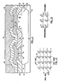
- Figure 1 is a cross-sectional view of a semiconductor structure which includes a P conductivity type silicon substrate 10 doped with boron to a resistivity of 1 to 3.5 ohms ⁇ cm.
- a buried layer 12 extends into substrate 10 and is doped with antimony to a peak concentration of approximately 3 ⁇ 1019 atoms per cubic centimeter.
- a thin epitaxial layer 15 is deposited, also of monocrystalline silicon.
- epitaxial layer 15 is approximately 1.1 microns thick and doped with phosphorus to a concentration of 1 ⁇ 1016 atoms per cubic centimeter.
- a channel stop implant 17 is introduced prior to the epitaxial layer deposition in regions where field oxide will be formed to prevent channel inversion at the silicon dioxide/silicon interface.
- regions of epitaxial silicon 15 are masked with silicon nitride, and a silicon etch is performed.
- a high temperature oxidation is used to create fully recessed field oxide regions 21 and 22.
- region 21 is annular and surrounds an island 23 of epitaxial silicon 15, to thereby provide an electrically-isolated pocket within which active and/or passive devices may be formed.
- Another portion of field oxide 22 separates a collector sink 25 from the remainder of the to-be-formed transistor.
- the collector sink 25 is heavily doped with N type impurity, typically phosphorus, to thereby provide a connection between surface 28 and buried layer 12. Because buried layer 12 is the collector of the bipolar transistor, a connection to collector sink 25 at surface 28 is a collector contact for the transistor.
- the base is implanted with P-type impurity and has a concentration of about 2 ⁇ 1018 atoms per cubic centimeter at a depth of 0.22 microns.
- the emitter 30 is doped. The transistor thereby created has emitter 30, base 15 and collector 12.
- a first layer of metal contacts 34 and 35 are deposited and defined using well known photolithographic techniques. Metal lines 34 provide the bit lines for the array and extend perpendicular to the plane of the drawing of Figure 1.
- An intermediate dielectric 36 is next deposited over the first layer metal, and using well known techniques, via openings 37 are provided. Then a second metal layer 43 is deposited and defined to provide word lines for the array. Contact 35 to the collector sink 25 provides a connection to the fuse for the word line 43 which extends perpendicular to the bit line 34 in the same plane as the bit lines.
- the base region is completely surrounded by silicon dioxide field regions 21 and 22.
- the emitter 30 is doped with arsenic and has an electrically active impurity concentration of 3 ⁇ 1019 atoms per cubic centimeter at its upper surface 28, and a total chemical impurity concentration of 8 ⁇ 1019 atoms per cubic centimeter.
- the emitter is approximately 0.21 microns deep, while the metal contacts 35 are comprised of 4%. copper and 0.9%. silicon, by weight, with about 95.1% aluminum.
- the lower doping of the emitter 30 is critical to my invention and, as discussed, provides several advantages with respect to prior art fuses.
- FIG. 2 is a schematic diagram illustrating how an array of the individual fuses of Figure 1 is interconnected.
- Each fuse structure of Figure 1 occupies one position in the array of Figure 2 and includes connections to both a bit line 34 and a word line 43. Because each fuse consists of a floating base NPN transistor, no connection is needed to the base region.
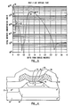
- Figure 3 is a graph illustrating the relationship of impurity concentration as a function of depth below the silicon surface 28 through the emitter 30, base 18, collector 12, and substrate 10.
- the arsenic impurity predominates with a chemical concentration of approximately 8 ⁇ 1019 atoms per cubic centimeter.
- the emitter concentration has fallen to less than 2 ⁇ 1017 atoms per cubic centimeter.
- the P type base impurity dominates the N type emitter impurity from approximately 0.21 microns into the structure to approximately 0.67 microns.
- the maximum doping for the base is approximately 2 ⁇ 1018 atoms per cubic centimeter at a depth of about 0.22 microns.
- the impurity concentration of collector 12 dominates. This reflects the upward diffusion of the collector impurity into the epitaxial layer by about 0.3 microns during the oxidation process used to form field oxide regions 21 and 22. The collector impurity continues to dominate to a depth of about 3 microns when the impurity for the substrate 10 is reached. Approximately 0.15 microns of N-epi lies under the base, prior to the upward diffusion of the N+ buried layer.
- Figure 4 is a cross section of the emitter 30, base 18, and buried layer 12 illustrating the fusing action of the structure of Figure 1.
- the structure of Figure 1 Prior to blowing the fuse, the structure of Figure 1, using the dimensions and impurity concentration specified, has an emitter-collector breakdown voltage of approximately 3.5 volts and a collector-emitter breakdown voltage of about 19 volts.
- Programming the structure is accomplished by applying current or voltage pulse to the emitter in an emitter-collector breakdown mode. For programming, the current will be about 45 milliamps for approximately 2.7 microseconds, with a resulting energy of 1.35 microJoules and a power of about 360 milliWatts.
- this pulse will be a ramped pulse from 0 to 6.3 volts in about 500 nanoseconds.
- the interface between metal 34 and silicon 30 is heated to its eutectic melting point of about 555°C, allowing the silicon to rapidly dissolve into the metal, leaving behind a void which mass transport of the metal fills.
- the result is a spike 40 which extends through the emitter-base junction 38 to short metal contact 35 to base 18.
- the pulse is discontinued when a voltage drop is detected.
- the collector-base breakdown voltage will be about 24 volts. At 100 microamps the forward voltage will be 0.87 volts, and the series resistance will be 115 ohms.
- Figure 5 is a schematic illustrating an array of fuses, some of which have been programmed.
- the unprogrammed fuses are represented as floating base transistors while the programmed fuses are shown as collector-base diodes.
- Appropriate well known circuitry coupled to the word and bit lines of the array in Figure 5 will detect the programmed and unprogrammed fuses. This circuitry can then interpret and supply to other circuitry suitable signals indicative of the "1" or "0" detected.
- the vertical fuse of my invention is particularly advantageous because it employs a low dose emitter without P type enhancement to thereby provide lower programming currents, higher collector-emitter and collector-base breakdown voltage, and lower collector-base capacitance.
- the emitter has a small volume so only a low programming current is required.
- the lower power allows faster programming, an important advantage for large arrays.
- heat treatments of 450°C for 60 minutes show no evidence of causing the aluminum contact 35 to prematurely cause a spike through the shallow emitter 30.
- the wider base width helps prevent overblowing the fuse. Life tests of programmed fuses at 200°C for 9 days does not cause any appreciable increase in series resistance.
- the implanted emitter on the fuse of my invention is more controllable and reliable than the diffused emitters of the prior art.
- the implantation of the emitter with a light dose of impurity increases the emitter resistance and helps retain heat near the metal/silicon interface, facilitating lower programming power.
- my fuse displays higher BV eco and BV ceo than the prior art. The higher voltages prevent unwanted parasitic leakage between adjacent word lines within an array.
Landscapes
- Design And Manufacture Of Integrated Circuits (AREA)
- Semiconductor Memories (AREA)
- Bipolar Transistors (AREA)
- Fuses (AREA)
Applications Claiming Priority (2)
| Application Number | Priority Date | Filing Date | Title |
|---|---|---|---|
| US90236986A | 1986-08-29 | 1986-08-29 | |
| US902369 | 1986-08-29 |
Publications (2)
| Publication Number | Publication Date |
|---|---|
| EP0258149A2 true EP0258149A2 (fr) | 1988-03-02 |
| EP0258149A3 EP0258149A3 (fr) | 1988-10-05 |
Family
ID=25415766
Family Applications (1)
| Application Number | Title | Priority Date | Filing Date |
|---|---|---|---|
| EP87401928A Withdrawn EP0258149A3 (fr) | 1986-08-29 | 1987-08-25 | Fusible vertical à émetteur faiblement dopé |
Country Status (4)
| Country | Link |
|---|---|
| EP (1) | EP0258149A3 (fr) |
| JP (1) | JPS63119255A (fr) |
| KR (1) | KR900006354B1 (fr) |
| CA (1) | CA1284232C (fr) |
Cited By (1)
| Publication number | Priority date | Publication date | Assignee | Title |
|---|---|---|---|---|
| US6252292B1 (en) | 1999-06-09 | 2001-06-26 | International Business Machines Corporation | Vertical electrical cavity-fuse |
Families Citing this family (2)
| Publication number | Priority date | Publication date | Assignee | Title |
|---|---|---|---|---|
| US5298784A (en) * | 1992-03-27 | 1994-03-29 | International Business Machines Corporation | Electrically programmable antifuse using metal penetration of a junction |
| DE19926107C1 (de) * | 1999-06-08 | 2000-11-16 | Siemens Ag | Halbleiteranordnung mit einer Fuse und ihr Herstellungsverfahren |
Family Cites Families (3)
| Publication number | Priority date | Publication date | Assignee | Title |
|---|---|---|---|---|
| FR2369652A1 (fr) * | 1976-10-29 | 1978-05-26 | Radiotechnique Compelec | Memoire morte programmable a transistors |
| JPS57188865A (en) * | 1981-05-18 | 1982-11-19 | Hitachi Ltd | Semiconductor memory cell |
| CA1188418A (fr) * | 1982-01-04 | 1985-06-04 | Jay A. Shideler | Procede d'isolement par oxyde pour memoires vives ou memoires mortes programmables standard avec memoire vive comprenant un transistor pnp lateral |
-
1987
- 1987-08-20 KR KR1019870009095A patent/KR900006354B1/ko not_active Expired
- 1987-08-24 CA CA000545195A patent/CA1284232C/fr not_active Expired - Fee Related
- 1987-08-25 EP EP87401928A patent/EP0258149A3/fr not_active Withdrawn
- 1987-08-28 JP JP62213173A patent/JPS63119255A/ja active Pending
Cited By (1)
| Publication number | Priority date | Publication date | Assignee | Title |
|---|---|---|---|---|
| US6252292B1 (en) | 1999-06-09 | 2001-06-26 | International Business Machines Corporation | Vertical electrical cavity-fuse |
Also Published As
| Publication number | Publication date |
|---|---|
| CA1284232C (fr) | 1991-05-14 |
| KR900006354B1 (ko) | 1990-08-28 |
| JPS63119255A (ja) | 1988-05-23 |
| EP0258149A3 (fr) | 1988-10-05 |
| KR880003364A (ko) | 1988-05-16 |
Similar Documents
| Publication | Publication Date | Title |
|---|---|---|
| US5045916A (en) | Extended silicide and external contact technology | |
| US4920396A (en) | CMOS having buried layer for carrier recombination | |
| US5144404A (en) | Polysilicon Schottky clamped transistor and vertical fuse devices | |
| US4420820A (en) | Programmable read-only memory | |
| JP3180831B2 (ja) | 絶縁ゲート制御半導体装置 | |
| US4458158A (en) | IC Including small signal and power devices | |
| EP0008946B1 (fr) | Dispositif de mémoire à semi-conducteur | |
| US5436496A (en) | Vertical fuse device | |
| US5059555A (en) | Method to fabricate vertical fuse devices and Schottky diodes using thin sacrificial layer | |
| EP0190070B1 (fr) | Structure à semi-conducteurs | |
| US5179432A (en) | Integrated PNP power bipolar transistor with low injection into substrate | |
| JPH0626253B2 (ja) | 長さの短い拡散領域を含む半導体素子の製造方法 | |
| JP2680788B2 (ja) | 集積化構造の能動クランプ装置 | |
| US4399450A (en) | ROM With poly-Si to mono-Si diodes | |
| US4516223A (en) | High density bipolar ROM having a lateral PN diode as a matrix element and method of fabrication | |
| US5212102A (en) | Method of making polysilicon Schottky clamped transistor and vertical fuse devices | |
| EP0018173B1 (fr) | Dispositif de mémoire morte programmable | |
| EP0043007B1 (fr) | Structure de circuit à transistors bipolaires à saturation limitée et méthode de fabrication correspondante | |
| US6828650B2 (en) | Bipolar junction transistor structure with improved current gain characteristics | |
| JPH09181315A (ja) | 半導体デバイス | |
| CA1284232C (fr) | Fusible vertical a emetteur faiblement dope | |
| EP0178968B1 (fr) | Logique à transistors à couplage de base | |
| US6445058B1 (en) | Bipolar junction transistor incorporating integral field plate | |
| US5055417A (en) | Process for fabricating self-aligned high performance lateral action silicon-controlled rectifier and static random access memory cells | |
| EP0075678B1 (fr) | Dispositif semi-conducteur à diode Schottky |
Legal Events
| Date | Code | Title | Description |
|---|---|---|---|
| PUAI | Public reference made under article 153(3) epc to a published international application that has entered the european phase |
Free format text: ORIGINAL CODE: 0009012 |
|
| AK | Designated contracting states |
Kind code of ref document: A2 Designated state(s): DE FR GB IT NL |
|
| PUAL | Search report despatched |
Free format text: ORIGINAL CODE: 0009013 |
|
| RHK1 | Main classification (correction) |
Ipc: H01L 27/10 |
|
| AK | Designated contracting states |
Kind code of ref document: A3 Designated state(s): DE FR GB IT NL |
|
| 17P | Request for examination filed |
Effective date: 19890329 |
|
| 17Q | First examination report despatched |
Effective date: 19910905 |
|
| STAA | Information on the status of an ep patent application or granted ep patent |
Free format text: STATUS: THE APPLICATION IS DEEMED TO BE WITHDRAWN |
|
| 18D | Application deemed to be withdrawn |
Effective date: 19930427 |
|
| RIN1 | Information on inventor provided before grant (corrected) |
Inventor name: JEROME, RICK C. |