EP0258606A2 - Verfahren zur Herstellung von thermischen Tintenstrahl-Druckköpfen und damit hergestellter Dünnfilmwiderstands-Druckkopf - Google Patents
Verfahren zur Herstellung von thermischen Tintenstrahl-Druckköpfen und damit hergestellter Dünnfilmwiderstands-Druckkopf Download PDFInfo
- Publication number
- EP0258606A2 EP0258606A2 EP87110583A EP87110583A EP0258606A2 EP 0258606 A2 EP0258606 A2 EP 0258606A2 EP 87110583 A EP87110583 A EP 87110583A EP 87110583 A EP87110583 A EP 87110583A EP 0258606 A2 EP0258606 A2 EP 0258606A2
- Authority
- EP
- European Patent Office
- Prior art keywords
- conductive trace
- area
- pattern
- trace pattern
- insulating substrate
- Prior art date
- Legal status (The legal status is an assumption and is not a legal conclusion. Google has not performed a legal analysis and makes no representation as to the accuracy of the status listed.)
- Granted
Links
- 238000000034 method Methods 0.000 title claims abstract description 10
- 239000010409 thin film Substances 0.000 title claims description 5
- 238000004519 manufacturing process Methods 0.000 title abstract description 7
- 239000000463 material Substances 0.000 claims abstract description 45
- 230000004888 barrier function Effects 0.000 claims abstract description 22
- 239000000758 substrate Substances 0.000 claims abstract description 20
- 229910052751 metal Inorganic materials 0.000 claims abstract description 12
- 239000002184 metal Substances 0.000 claims abstract description 12
- 239000010410 layer Substances 0.000 description 50
- 229910052782 aluminium Inorganic materials 0.000 description 19
- XAGFODPZIPBFFR-UHFFFAOYSA-N aluminium Chemical compound [Al] XAGFODPZIPBFFR-UHFFFAOYSA-N 0.000 description 18
- 229910052581 Si3N4 Inorganic materials 0.000 description 9
- 239000002131 composite material Substances 0.000 description 9
- HBMJWWWQQXIZIP-UHFFFAOYSA-N silicon carbide Chemical compound [Si+]#[C-] HBMJWWWQQXIZIP-UHFFFAOYSA-N 0.000 description 8
- 229910010271 silicon carbide Inorganic materials 0.000 description 8
- HQVNEWCFYHHQES-UHFFFAOYSA-N silicon nitride Chemical compound N12[Si]34N5[Si]62N3[Si]51N64 HQVNEWCFYHHQES-UHFFFAOYSA-N 0.000 description 8
- VYPSYNLAJGMNEJ-UHFFFAOYSA-N Silicium dioxide Chemical compound O=[Si]=O VYPSYNLAJGMNEJ-UHFFFAOYSA-N 0.000 description 7
- PCHJSUWPFVWCPO-UHFFFAOYSA-N gold Chemical compound [Au] PCHJSUWPFVWCPO-UHFFFAOYSA-N 0.000 description 7
- 229910052737 gold Inorganic materials 0.000 description 7
- 239000010931 gold Substances 0.000 description 7
- RVSGESPTHDDNTH-UHFFFAOYSA-N alumane;tantalum Chemical compound [AlH3].[Ta] RVSGESPTHDDNTH-UHFFFAOYSA-N 0.000 description 5
- 239000004020 conductor Substances 0.000 description 5
- 238000010276 construction Methods 0.000 description 4
- 229910052715 tantalum Inorganic materials 0.000 description 4
- GUVRBAGPIYLISA-UHFFFAOYSA-N tantalum atom Chemical compound [Ta] GUVRBAGPIYLISA-UHFFFAOYSA-N 0.000 description 4
- 238000005260 corrosion Methods 0.000 description 3
- 230000007797 corrosion Effects 0.000 description 3
- 239000000377 silicon dioxide Substances 0.000 description 3
- 235000012239 silicon dioxide Nutrition 0.000 description 3
- 229910004490 TaAl Inorganic materials 0.000 description 2
- 239000004411 aluminium Substances 0.000 description 2
- 238000005336 cracking Methods 0.000 description 2
- 238000005530 etching Methods 0.000 description 2
- 239000002861 polymer material Substances 0.000 description 2
- 238000006748 scratching Methods 0.000 description 2
- 230000002393 scratching effect Effects 0.000 description 2
- 229910052710 silicon Inorganic materials 0.000 description 2
- 239000010703 silicon Substances 0.000 description 2
- XUIMIQQOPSSXEZ-UHFFFAOYSA-N Silicon Chemical compound [Si] XUIMIQQOPSSXEZ-UHFFFAOYSA-N 0.000 description 1
- FRIKWZARTBPWBN-UHFFFAOYSA-N [Si].O=[Si]=O Chemical compound [Si].O=[Si]=O FRIKWZARTBPWBN-UHFFFAOYSA-N 0.000 description 1
- BROYGXJPKIABKM-UHFFFAOYSA-N [Ta].[Au] Chemical compound [Ta].[Au] BROYGXJPKIABKM-UHFFFAOYSA-N 0.000 description 1
- 230000015572 biosynthetic process Effects 0.000 description 1
- 230000007547 defect Effects 0.000 description 1
- 238000000151 deposition Methods 0.000 description 1
- 230000001627 detrimental effect Effects 0.000 description 1
- 230000009189 diving Effects 0.000 description 1
- 239000010408 film Substances 0.000 description 1
- 238000007641 inkjet printing Methods 0.000 description 1
- 239000011810 insulating material Substances 0.000 description 1
- 238000009413 insulation Methods 0.000 description 1
- 230000000873 masking effect Effects 0.000 description 1
- 238000001883 metal evaporation Methods 0.000 description 1
- 238000012986 modification Methods 0.000 description 1
- 230000004048 modification Effects 0.000 description 1
- 230000003647 oxidation Effects 0.000 description 1
- 238000007254 oxidation reaction Methods 0.000 description 1
- TWNQGVIAIRXVLR-UHFFFAOYSA-N oxo(oxoalumanyloxy)alumane Chemical compound O=[Al]O[Al]=O TWNQGVIAIRXVLR-UHFFFAOYSA-N 0.000 description 1
- 230000002093 peripheral effect Effects 0.000 description 1
- 239000011241 protective layer Substances 0.000 description 1
- 238000009877 rendering Methods 0.000 description 1
- 230000035945 sensitivity Effects 0.000 description 1
- 239000002153 silicon-carbon composite material Substances 0.000 description 1
- 239000007858 starting material Substances 0.000 description 1
- 238000007740 vapor deposition Methods 0.000 description 1
Images


Classifications
-
- B—PERFORMING OPERATIONS; TRANSPORTING
- B41—PRINTING; LINING MACHINES; TYPEWRITERS; STAMPS
- B41J—TYPEWRITERS; SELECTIVE PRINTING MECHANISMS, i.e. MECHANISMS PRINTING OTHERWISE THAN FROM A FORME; CORRECTION OF TYPOGRAPHICAL ERRORS
- B41J2/00—Typewriters or selective printing mechanisms characterised by the printing or marking process for which they are designed
- B41J2/005—Typewriters or selective printing mechanisms characterised by the printing or marking process for which they are designed characterised by bringing liquid or particles selectively into contact with a printing material
- B41J2/01—Ink jet
- B41J2/135—Nozzles
- B41J2/16—Production of nozzles
- B41J2/1621—Manufacturing processes
- B41J2/164—Manufacturing processes thin film formation
- B41J2/1642—Manufacturing processes thin film formation thin film formation by CVD [chemical vapor deposition]
-
- B—PERFORMING OPERATIONS; TRANSPORTING
- B41—PRINTING; LINING MACHINES; TYPEWRITERS; STAMPS
- B41J—TYPEWRITERS; SELECTIVE PRINTING MECHANISMS, i.e. MECHANISMS PRINTING OTHERWISE THAN FROM A FORME; CORRECTION OF TYPOGRAPHICAL ERRORS
- B41J2/00—Typewriters or selective printing mechanisms characterised by the printing or marking process for which they are designed
- B41J2/005—Typewriters or selective printing mechanisms characterised by the printing or marking process for which they are designed characterised by bringing liquid or particles selectively into contact with a printing material
- B41J2/01—Ink jet
- B41J2/135—Nozzles
- B41J2/14—Structure thereof only for on-demand ink jet heads
- B41J2/14016—Structure of bubble jet print heads
- B41J2/14088—Structure of heating means
- B41J2/14112—Resistive element
- B41J2/14129—Layer structure
-
- B—PERFORMING OPERATIONS; TRANSPORTING
- B41—PRINTING; LINING MACHINES; TYPEWRITERS; STAMPS
- B41J—TYPEWRITERS; SELECTIVE PRINTING MECHANISMS, i.e. MECHANISMS PRINTING OTHERWISE THAN FROM A FORME; CORRECTION OF TYPOGRAPHICAL ERRORS
- B41J2/00—Typewriters or selective printing mechanisms characterised by the printing or marking process for which they are designed
- B41J2/005—Typewriters or selective printing mechanisms characterised by the printing or marking process for which they are designed characterised by bringing liquid or particles selectively into contact with a printing material
- B41J2/01—Ink jet
- B41J2/135—Nozzles
- B41J2/16—Production of nozzles
- B41J2/1601—Production of bubble jet print heads
- B41J2/1603—Production of bubble jet print heads of the front shooter type
-
- B—PERFORMING OPERATIONS; TRANSPORTING
- B41—PRINTING; LINING MACHINES; TYPEWRITERS; STAMPS
- B41J—TYPEWRITERS; SELECTIVE PRINTING MECHANISMS, i.e. MECHANISMS PRINTING OTHERWISE THAN FROM A FORME; CORRECTION OF TYPOGRAPHICAL ERRORS
- B41J2/00—Typewriters or selective printing mechanisms characterised by the printing or marking process for which they are designed
- B41J2/005—Typewriters or selective printing mechanisms characterised by the printing or marking process for which they are designed characterised by bringing liquid or particles selectively into contact with a printing material
- B41J2/01—Ink jet
- B41J2/135—Nozzles
- B41J2/16—Production of nozzles
- B41J2/1621—Manufacturing processes
- B41J2/1626—Manufacturing processes etching
- B41J2/1628—Manufacturing processes etching dry etching
-
- B—PERFORMING OPERATIONS; TRANSPORTING
- B41—PRINTING; LINING MACHINES; TYPEWRITERS; STAMPS
- B41J—TYPEWRITERS; SELECTIVE PRINTING MECHANISMS, i.e. MECHANISMS PRINTING OTHERWISE THAN FROM A FORME; CORRECTION OF TYPOGRAPHICAL ERRORS
- B41J2/00—Typewriters or selective printing mechanisms characterised by the printing or marking process for which they are designed
- B41J2/005—Typewriters or selective printing mechanisms characterised by the printing or marking process for which they are designed characterised by bringing liquid or particles selectively into contact with a printing material
- B41J2/01—Ink jet
- B41J2/135—Nozzles
- B41J2/16—Production of nozzles
- B41J2/1621—Manufacturing processes
- B41J2/1631—Manufacturing processes photolithography
-
- B—PERFORMING OPERATIONS; TRANSPORTING
- B41—PRINTING; LINING MACHINES; TYPEWRITERS; STAMPS
- B41J—TYPEWRITERS; SELECTIVE PRINTING MECHANISMS, i.e. MECHANISMS PRINTING OTHERWISE THAN FROM A FORME; CORRECTION OF TYPOGRAPHICAL ERRORS
- B41J2/00—Typewriters or selective printing mechanisms characterised by the printing or marking process for which they are designed
- B41J2/005—Typewriters or selective printing mechanisms characterised by the printing or marking process for which they are designed characterised by bringing liquid or particles selectively into contact with a printing material
- B41J2/01—Ink jet
- B41J2/135—Nozzles
- B41J2/16—Production of nozzles
- B41J2/1621—Manufacturing processes
- B41J2/164—Manufacturing processes thin film formation
- B41J2/1646—Manufacturing processes thin film formation thin film formation by sputtering
-
- Y—GENERAL TAGGING OF NEW TECHNOLOGICAL DEVELOPMENTS; GENERAL TAGGING OF CROSS-SECTIONAL TECHNOLOGIES SPANNING OVER SEVERAL SECTIONS OF THE IPC; TECHNICAL SUBJECTS COVERED BY FORMER USPC CROSS-REFERENCE ART COLLECTIONS [XRACs] AND DIGESTS
- Y10—TECHNICAL SUBJECTS COVERED BY FORMER USPC
- Y10T—TECHNICAL SUBJECTS COVERED BY FORMER US CLASSIFICATION
- Y10T29/00—Metal working
- Y10T29/49—Method of mechanical manufacture
- Y10T29/49002—Electrical device making
- Y10T29/49082—Resistor making
- Y10T29/49099—Coating resistive material on a base
Definitions
- This invention relates generally to thermal ink jet printhead construction and more particularly to an improved integrated interconnect circuit extending between the printhead heater resistors and external pulse drive circuitry for supplying drive current to these heater resistors.
- TFR thin film resistor
- the resistive heater --layer material may, for example, be tantalum-aluminum, TaAl.
- the conductive trace pattern is most typically aluminiu, although it could also be gold or other conductive material compatible with the other materials in the materials set for the printhead.
- an inert barrier layer such as a composite layer of silicon nitride and silicon carbide in order to protect the underlying layers from cavitation wear and ink corrosion.
- one standard prior art approach involved etching a relatively large opening or via in the silicon nitride/silicon carbide composite barrier layer and then forming a relatively large contact pad in this opening to thus make contact with the underlying aluminum trace conductor material. Then, wire bonding or pressure contact connections could be made to this relatively large contact pad to provide an electrical current path into the aluminum trace material and to the ink jet heater resistors.
- the above prior art structure is possessed with several disadvantages associated with the relatively large opening or via in the insulating barrier layer and directly over the aluminum conductive trace layer.
- the first of these disadvantages resides in the fact that the large via in the silicon nitride/silicon carbide composite layer exposes a relatively large sidewall area of these materials. This large area sidewall exposure means -increasing the area in which pinholes or cracks might possibly occur and thus produce electrical shorts in the barrier layer.
- Another disadvantage of the above prior art electrical interconnect approach involves exposing a relatively large area of the aluminum trace material in order to provide the desired wide area contact pad thereover.
- the exposure of such a large area of aluminum trace material in the manufacturing process increases the possibility of forming aluminum oxide, A1 2 0 3 , on the conductive trace material and thus rendering it insulating or partially insulating instead of fully conducting.
- Another disadvantage of using the above prior art approach resides in the increased probability of undercutting the silicon nitride and silicon carbide layers during the etching of the via therein. Again, such increased probability is caused by the exposure of the relatively wide area sidewall of the silicon nitride/silicon carbide barrier defining the via.
- Another disadvantage of using the prior art approach described above relates to the formation of a non- flat dish-shaped contact pad directly over the aluminum trace material.
- This geometry and structure increases the likelihood of scratching the edge of the printhead structure immediately adjacent the conducting trace material, and such scratching in turn increases the likelihood of producing electrical shorts down through the printhead structure to the aluminum conductive trace material.
- the dish shape or non-planar contour of the contact pad makes it difficult to make certain types of electrical connections to the printhead structure, e.g. spring biased pressure connections from a lead frame-type of flexible circuit.
- a further disadvantage of using the above prior approach relates to the sensitivity of chipping and cracking at the edges of the multiple layers of materials over which the dish-shaped contact is placed. This chipping and cracking will cause corrosion of these materials at their outer edges, but this does not occur in devices manufactured by the present invention where the lead-in contacts have been removed from pressure contact at the edges of these interior layered materials.
- the general purpose of this invention is to provide a new and improved integrated circuit interconnect structure for providing drive current to thermal ink jet printhead heater resistors and a high yield -process for fabricating same.
- This interconnect structure is uniquely adapted and constructed for making good electrical connections to spring biased pressure contacts, such as individual fingers or leads on a lead frame type of flexible or "flex" circuit.
- a printhead structure and fabrication process therefor which includes forming a resistive layer on an insulating substrate and then forming a conductive trace pattern laterally coextensive with the resistive layer and extending only over a predetermined area of the insulating substrate.
- the conductive trace pattern has an opening therein defining a resistor heater element.
- an insulating barrier layer is formed atop the conductive trace material and extends down over the edges of the conductive trace material and the resisitive layer and then out over a predetermined area of the adjacent insulating substrate.
- a small via is formed in the insulating barrier layer and over the conductive trace pattern, so that a subsequently deposited metal overlay pattern may be extended from into the via and then out over the adjacent area of the insula-_ ting substrate where no conductive trace material extends.
- the interconnect metal in this latter area provides a relatively large and flat electrical contact area for spring biased contacts.
- the electrical connection to the conductive trace pattern is only through the relatively small via in the barrier layer where the area.of edge -. exposure in the barrier layer and the area of conductive trace material exposure is maintained at a minimum.
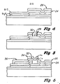
- Figures 1 through 7 illustrate, in schematic cross section, a series of thin film resistor process steps utilized in fabricating a printhead interconnect structure according to the invention.
- Figure 8 is an alternative embodiment of the invention wherein the barrier layers have been laterally reduced to expose an edge portion of the underlying aluminum trace material for subsequent metal overlay thereon.
- a substrate starting material 10 such as silicon is treated using either thermal oxidation or vapor deposition techniques to form a thin layer 12 of silicon dioxide thereon.
- the combination of the- silicon substrate 10 and the layer 12 of silicon dioxide will be referred to herein as the "insulating substrate" upon which a subsequent layer 14 of resisitive heater material is deposited.
- the layer 14 will be tantalum aluminum, TaAl, which is a well known resistive heater material in the art of thermal ink jet printhead construction.
- a thin layer 16 of-aluminum is deposited atop the tantalum aluminum layer 14 to complete the structure of Figure 1.
- the silicon- silicon dioxide combination 10, 12 was approximately 600 microns in thickness; the tantalum aluminum layer 14 was approximately 1000 angstroms in thickness; and the aluminum conductive trace material 16 was approximately 5000 angstroms in thickness.
- the resistor and conductor materials were magetron sputter deposited. This materials set is generally well known in the art and is described, for example, in the Hewlett-Packard Journal, Vol. 36, No. 5, May, 1 985, incorporated herein by reference.
- the structure shown therein was appropriately masked and etched with a suitable etchant in order to define the composite island 18 of tantalum aluminum 14 and aluminum 16 on the right hand side of the insulating substrate.
- the island 18 is formed on only a portion of the insulating substrate 10 and 12, leaving an area of the lefthand side of the substrate available for making good electrical contacts of the type to be described.
- a pattern is etched in the aluminum layer 16 to form the opening 20 which defines the lateral extent of a resistive heater element 22 which is current driven by the conductive trace aluminum layer 16.
- a composite layer barrier material is deposited over the upper surface of the structure in this figure and includes a first layer 24 of silicon nitride which is covered by a second layer of highly inert silicon carbide.
- This composite layer (24, 26) barrier material provides both good adherance to the underlying materials and good insulation and protection against cava- tion wear and ink corrosion which the underlying layers beneath these materials 24 and 26 would otherwise receive during an ink jet printing operation.
- a relatively small via 28 is dry etched in the composite silicon nitride/silicon carbide barrier layer using freon gas to thereby leave a small area 30 in the aluminum conductive trace material exposed for further electrical contact.
- Such contact is made as shown in Figure 6 when a conductive lead-in or overlay pattern of conductors 32 and 34 are magnetron sputter deposited on the surface of Figure 5 and extend from into electrical contact with a relatively small area 30 of conductor trace material and then out onto the left hand side of the structure in Figure 5 and atop the previously- deposited barrier layer material.
- the combined thickness of the gold and tantalum layers is approximately 2 microns.
- This conductive lead-in composite structure includes a first layer 32 of tantalum and a second layer 34 of gold successively deposited in the geometrical configuration shown using conventional masking and metal evaporation techniques.
- the area 36 on the upper surface of the gold layer 34 in Figure 6 extends over a relatively wide and flat area of the integrated structure and is located away from the aluminium conductive trace pattern previously described.
- This construction therefore enables a finger or spring lead contact member 38, which may be part of a larger lead frame member (not shown), to be brought into good firm pressure contact with the surface area 36 of the gold layer 34 and without causing any detrimental effect on the aluminum conductive trace pattern.
- This larger lead frame member is described in more detail in copending application of Janet E. Mebane et al Serial No. (ID 186201) and assigned to the present assignee.
- a surface pattern of polymer material 40 is formed in the geometry shown in Figure 7 to a thickness of approximately 50 microns.
- This polymer material provides a protective layer or shield over the contact via 30 and over the electrical contact layers 3 2 and 34 extending down into contact therewith.
- the S i 3 N 4/ Si C composite layer 24', 26' is masked and etched so as to leave a small edge portion of the aluminium trace material 16' exposed to receive the tantalum layer 32' thereon as shown in Figure 8. And, as in Figure 7, there is a relatively wide area on the surface of the gold film 34' for recieving the spring biased lead contact 38'.
- the present invention is used in the fabrication of printheads for thermal ink jet printers which serve as standard peripheral equipment for a variety of computers and the like.
Landscapes
- Engineering & Computer Science (AREA)
- Manufacturing & Machinery (AREA)
- Particle Formation And Scattering Control In Inkjet Printers (AREA)
Applications Claiming Priority (2)
| Application Number | Priority Date | Filing Date | Title |
|---|---|---|---|
| US06/902,287 US4862197A (en) | 1986-08-28 | 1986-08-28 | Process for manufacturing thermal ink jet printhead and integrated circuit (IC) structures produced thereby |
| US902287 | 1986-08-28 |
Publications (3)
| Publication Number | Publication Date |
|---|---|
| EP0258606A2 true EP0258606A2 (de) | 1988-03-09 |
| EP0258606A3 EP0258606A3 (en) | 1989-07-26 |
| EP0258606B1 EP0258606B1 (de) | 1992-11-19 |
Family
ID=25415615
Family Applications (1)
| Application Number | Title | Priority Date | Filing Date |
|---|---|---|---|
| EP87110583A Expired - Lifetime EP0258606B1 (de) | 1986-08-28 | 1987-07-22 | Verfahren zur Herstellung von thermischen Tintenstrahl-Druckköpfen und damit hergestellter Dünnfilmwiderstands-Druckkopf |
Country Status (6)
| Country | Link |
|---|---|
| US (1) | US4862197A (de) |
| EP (1) | EP0258606B1 (de) |
| JP (1) | JP2960065B2 (de) |
| CA (1) | CA1277774C (de) |
| DE (1) | DE3782700T2 (de) |
| HK (1) | HK128393A (de) |
Cited By (3)
| Publication number | Priority date | Publication date | Assignee | Title |
|---|---|---|---|---|
| EP0380366A3 (de) * | 1989-01-27 | 1991-02-13 | Canon Kabushiki Kaisha | Trägerschicht für Aufzeichnungskopf und Aufzeichnungskopf |
| EP0525787A3 (en) * | 1991-08-01 | 1993-05-19 | Canon Kabushiki Kaisha | Method for manufacturing a recording head |
| EP0500069A3 (en) * | 1991-02-20 | 1993-06-09 | Canon Kabushiki Kaisha | Method for etching silicon compound film and process for forming article by utilizing the method |
Families Citing this family (68)
| Publication number | Priority date | Publication date | Assignee | Title |
|---|---|---|---|---|
| DE68917790T2 (de) * | 1988-06-03 | 1995-01-05 | Canon Kk | Aufzeichnungskopf mit Flüssigkeitsemission, Substrat hierfür sowie Aufzeichnungsgerät mit Flüssigkeitsemission unter Verwendung dieses Kopfes. |
| US5243363A (en) * | 1988-07-22 | 1993-09-07 | Canon Kabushiki Kaisha | Ink-jet recording head having bump-shaped electrode and protective layer providing structural support |
| US5570119A (en) * | 1988-07-26 | 1996-10-29 | Canon Kabushiki Kaisha | Multilayer device having integral functional element for use with an ink jet recording apparatus, and recording apparatus |
| US4999650A (en) * | 1989-12-18 | 1991-03-12 | Eastman Kodak Company | Bubble jet print head having improved multiplex actuation construction |
| JP2771008B2 (ja) * | 1990-02-28 | 1998-07-02 | キヤノン株式会社 | 記録装置及び記録ヘッド |
| US5045870A (en) * | 1990-04-02 | 1991-09-03 | International Business Machines Corporation | Thermal ink drop on demand devices on a single chip with vertical integration of driver device |
| US5187500A (en) * | 1990-09-05 | 1993-02-16 | Hewlett-Packard Company | Control of energy to thermal inkjet heating elements |
| US5317346A (en) * | 1992-03-04 | 1994-05-31 | Hewlett-Packard Company | Compound ink feed slot |
| AU5604694A (en) * | 1992-11-12 | 1994-06-08 | Graphic Utilities, Inc. | Method for refilling ink jet cartridges |
| US5686948A (en) * | 1992-11-12 | 1997-11-11 | Graphic Utilities, Inc. | Method for refilling ink jet cartridges |
| DE69405435T2 (de) * | 1993-03-16 | 1998-01-22 | Hewlett Packard Co | Verfahren und Vorrichtung für die Herstellung von elektrisch zusammengeschalteten Schaltungen |
| EP0616394A1 (de) * | 1993-03-16 | 1994-09-21 | Hewlett-Packard Company | Verfahren und Vorrichtung für die Herstellung von elektrisch zusammengeschalteten Schaltungen |
| US5295839A (en) * | 1993-03-16 | 1994-03-22 | Hewlett-Packard Company | Method and system for interconnectingly engaging circuits |
| US5949461A (en) * | 1994-02-18 | 1999-09-07 | Nu-Kote Imaging International, Inc. | Ink refill bottle |
| US6070969A (en) | 1994-03-23 | 2000-06-06 | Hewlett-Packard Company | Thermal inkjet printhead having a preferred nucleation site |
| US5635968A (en) * | 1994-04-29 | 1997-06-03 | Hewlett-Packard Company | Thermal inkjet printer printhead with offset heater resistors |
| US6758552B1 (en) | 1995-12-06 | 2004-07-06 | Hewlett-Packard Development Company | Integrated thin-film drive head for thermal ink-jet printer |
| US5883650A (en) * | 1995-12-06 | 1999-03-16 | Hewlett-Packard Company | Thin-film printhead device for an ink-jet printer |
| US6239820B1 (en) | 1995-12-06 | 2001-05-29 | Hewlett-Packard Company | Thin-film printhead device for an ink-jet printer |
| US5790154A (en) * | 1995-12-08 | 1998-08-04 | Hitachi Koki Co., Ltd. | Method of manufacturing an ink ejection recording head and a recording apparatus using the recording head |
| US6113216A (en) | 1996-08-09 | 2000-09-05 | Hewlett-Packard Company | Wide array thermal ink-jet print head |
| US5901425A (en) | 1996-08-27 | 1999-05-11 | Topaz Technologies Inc. | Inkjet print head apparatus |
| EP0882978A1 (de) | 1997-06-04 | 1998-12-09 | STMicroelectronics S.r.l. | Integrierte Halbleitervorrichtung mit einem auf chemischer Widerstandsfähigkeit beruhenden Microgassensor und Verfahren zu deren Herstellung |
| US6030071A (en) * | 1997-07-03 | 2000-02-29 | Lexmark International, Inc. | Printhead having heating element conductors arranged in a matrix |
| US6120135A (en) * | 1997-07-03 | 2000-09-19 | Lexmark International, Inc. | Printhead having heating element conductors arranged in spaced apart planes and including heating elements having a substantially constant cross-sectional area in the direction of current flow |
| US6123410A (en) | 1997-10-28 | 2000-09-26 | Hewlett-Packard Company | Scalable wide-array inkjet printhead and method for fabricating same |
| TW468271B (en) * | 1999-03-26 | 2001-12-11 | United Microelectronics Corp | Thin film resistor used in a semiconductor chip and its manufacturing method |
| US6260952B1 (en) * | 1999-04-22 | 2001-07-17 | Hewlett-Packard Company | Apparatus and method for routing power and ground lines in a ink-jet printhead |
| US6132032A (en) * | 1999-08-13 | 2000-10-17 | Hewlett-Packard Company | Thin-film print head for thermal ink-jet printers |
| US6280019B1 (en) | 1999-08-30 | 2001-08-28 | Hewlett-Packard Company | Segmented resistor inkjet drop generator with current crowding reduction |
| US6318846B1 (en) | 1999-08-30 | 2001-11-20 | Hewlett-Packard Company | Redundant input signal paths for an inkjet print head |
| US6139131A (en) | 1999-08-30 | 2000-10-31 | Hewlett-Packard Company | High drop generator density printhead |
| US6582062B1 (en) | 1999-10-18 | 2003-06-24 | Hewlett-Packard Development Company, L.P. | Large thermal ink jet nozzle array printhead |
| US6331044B2 (en) * | 1999-10-27 | 2001-12-18 | Hewlett-Packard Company | Corrosion resistant thermal ink jet print cartridge and method of manufacturing same |
| JP2001138521A (ja) | 1999-11-11 | 2001-05-22 | Canon Inc | インクジェット記録ヘッドおよび該記録ヘッドを用いたインクジェット記録装置 |
| US6482574B1 (en) | 2000-04-20 | 2002-11-19 | Hewlett-Packard Co. | Droplet plate architecture in ink-jet printheads |
| US6481831B1 (en) | 2000-07-07 | 2002-11-19 | Hewlett-Packard Company | Fluid ejection device and method of fabricating |
| US6648732B2 (en) | 2001-01-30 | 2003-11-18 | Hewlett-Packard Development Company, L.P. | Thin film coating of a slotted substrate and techniques for forming slotted substrates |
| US20020158945A1 (en) | 2001-04-30 | 2002-10-31 | Miller Richard Todd | Heating element of a printhead having resistive layer over conductive layer |
| US7101021B2 (en) * | 2001-07-30 | 2006-09-05 | Seiko Epson Corporation | Connection apparatus for circuit board, ink jet type recording apparatus using the same, IC chip and ink cartridge having IC chip |
| US6856007B2 (en) | 2001-08-28 | 2005-02-15 | Tessera, Inc. | High-frequency chip packages |
| US7025894B2 (en) * | 2001-10-16 | 2006-04-11 | Hewlett-Packard Development Company, L.P. | Fluid-ejection devices and a deposition method for layers thereof |
| US6747684B2 (en) | 2002-04-10 | 2004-06-08 | Hewlett-Packard Development Company, L.P. | Laser triggered inkjet firing |
| US6704996B2 (en) | 2002-04-30 | 2004-03-16 | Lexmark International, Inc. | Method for making ink jet printheads |
| US6540334B1 (en) | 2002-04-30 | 2003-04-01 | Lexmark International, Inc. | Method for making ink jet printheads |
| US7104623B2 (en) * | 2002-06-07 | 2006-09-12 | Hewlett-Packard Development Company, L.P. | Fluid ejection system with photosensor activation of ejection element |
| US7083250B2 (en) * | 2002-06-07 | 2006-08-01 | Hewlett-Packard Development Company, L.P. | Fluid ejection and scanning assembly with photosensor activation of ejection elements |
| US6705701B2 (en) * | 2002-06-07 | 2004-03-16 | Hewlett-Packard Development Company, L.P. | Fluid ejection and scanning system with photosensor activation of ejection elements |
| US6799819B2 (en) | 2002-06-07 | 2004-10-05 | Hewlett-Packard Development Company, L.P. | Photosensor activation of an ejection element of a fluid ejection device |
| US6786575B2 (en) * | 2002-12-17 | 2004-09-07 | Lexmark International, Inc. | Ink jet heater chip and method therefor |
| US6794753B2 (en) * | 2002-12-27 | 2004-09-21 | Lexmark International, Inc. | Diffusion barrier and method therefor |
| RU2261498C2 (ru) * | 2003-06-05 | 2005-09-27 | Открытое акционерное общество "НИИ молекулярной электроники и завод "Микрон" | Способ изготовления принтерной головки с тонкопленочным резистором и принтерная головка |
| RU2263998C2 (ru) * | 2003-06-05 | 2005-11-10 | Открытое акционерное общество "НИИ молекулярной электроники и завод "Микрон" | Способ изготовления тонкопленочной структуры межсоединений принтерной головки с тонкопленочным резистором |
| US6972480B2 (en) | 2003-06-16 | 2005-12-06 | Shellcase Ltd. | Methods and apparatus for packaging integrated circuit devices |
| WO2005004195A2 (en) | 2003-07-03 | 2005-01-13 | Shellcase Ltd. | Method and apparatus for packaging integrated circuit devices |
| JP2005067164A (ja) * | 2003-08-28 | 2005-03-17 | Sony Corp | 液体吐出ヘッド、液体吐出装置及び液体吐出ヘッドの製造方法 |
| US7224056B2 (en) | 2003-09-26 | 2007-05-29 | Tessera, Inc. | Back-face and edge interconnects for lidded package |
| CN1314542C (zh) * | 2003-10-21 | 2007-05-09 | 财团法人工业技术研究院 | 一种喷液头芯片结构及其制造方法 |
| US20050116344A1 (en) * | 2003-10-29 | 2005-06-02 | Tessera, Inc. | Microelectronic element having trace formed after bond layer |
| US7080896B2 (en) * | 2004-01-20 | 2006-07-25 | Lexmark International, Inc. | Micro-fluid ejection device having high resistance heater film |
| JP4137027B2 (ja) * | 2004-08-16 | 2008-08-20 | キヤノン株式会社 | インクジェットヘッド用基板、該基板の製造方法および前記基板を用いるインクジェットヘッド |
| US20060183270A1 (en) * | 2005-02-14 | 2006-08-17 | Tessera, Inc. | Tools and methods for forming conductive bumps on microelectronic elements |
| US8143095B2 (en) | 2005-03-22 | 2012-03-27 | Tessera, Inc. | Sequential fabrication of vertical conductive interconnects in capped chips |
| US7291849B1 (en) * | 2005-09-28 | 2007-11-06 | Agere Systems Inc. | Calibration standard for transmission electron microscopy |
| US7936062B2 (en) | 2006-01-23 | 2011-05-03 | Tessera Technologies Ireland Limited | Wafer level chip packaging |
| US8604605B2 (en) | 2007-01-05 | 2013-12-10 | Invensas Corp. | Microelectronic assembly with multi-layer support structure |
| US8733872B2 (en) * | 2008-01-28 | 2014-05-27 | Hewlett-Packard Development Company, L.P. | Common base lateral bipolar junction transistor circuit for an inkjet print head |
| US11214064B2 (en) | 2018-04-02 | 2022-01-04 | Hewlett-Packard Development Company, L.P. | Adhering layers of fluidic dies |
Family Cites Families (5)
| Publication number | Priority date | Publication date | Assignee | Title |
|---|---|---|---|---|
| US4463359A (en) * | 1979-04-02 | 1984-07-31 | Canon Kabushiki Kaisha | Droplet generating method and apparatus thereof |
| JPS57211248A (en) * | 1981-06-22 | 1982-12-25 | Hitachi Ltd | Semiconductor integrated circuit device |
| JPH0645235B2 (ja) * | 1984-07-20 | 1994-06-15 | キヤノン株式会社 | 液体噴射ヘッドおよび該ヘッドの製造方法 |
| JPS6135973A (ja) * | 1984-07-30 | 1986-02-20 | Hitachi Ltd | 感熱ヘツド |
| US4719477A (en) * | 1986-01-17 | 1988-01-12 | Hewlett-Packard Company | Integrated thermal ink jet printhead and method of manufacture |
-
1986
- 1986-08-28 US US06/902,287 patent/US4862197A/en not_active Expired - Lifetime
-
1987
- 1987-07-22 EP EP87110583A patent/EP0258606B1/de not_active Expired - Lifetime
- 1987-07-22 DE DE8787110583T patent/DE3782700T2/de not_active Expired - Fee Related
- 1987-07-28 CA CA000543170A patent/CA1277774C/en not_active Expired - Lifetime
- 1987-08-28 JP JP62214925A patent/JP2960065B2/ja not_active Expired - Lifetime
-
1993
- 1993-11-18 HK HK1283/93A patent/HK128393A/en not_active IP Right Cessation
Cited By (5)
| Publication number | Priority date | Publication date | Assignee | Title |
|---|---|---|---|---|
| EP0380366A3 (de) * | 1989-01-27 | 1991-02-13 | Canon Kabushiki Kaisha | Trägerschicht für Aufzeichnungskopf und Aufzeichnungskopf |
| US5420623A (en) * | 1989-01-27 | 1995-05-30 | Canon Kabushiki Kaisha | Recording head having multi-layer wiring |
| EP0500069A3 (en) * | 1991-02-20 | 1993-06-09 | Canon Kabushiki Kaisha | Method for etching silicon compound film and process for forming article by utilizing the method |
| US5374332A (en) * | 1991-02-20 | 1994-12-20 | Canon Kabushiki Kaisha | Method for etching silicon compound film and process for forming article by utilizing the method |
| EP0525787A3 (en) * | 1991-08-01 | 1993-05-19 | Canon Kabushiki Kaisha | Method for manufacturing a recording head |
Also Published As
| Publication number | Publication date |
|---|---|
| JP2960065B2 (ja) | 1999-10-06 |
| EP0258606A3 (en) | 1989-07-26 |
| CA1277774C (en) | 1990-12-11 |
| DE3782700T2 (de) | 1993-06-03 |
| HK128393A (en) | 1993-11-26 |
| DE3782700D1 (de) | 1992-12-24 |
| JPS6359541A (ja) | 1988-03-15 |
| US4862197A (en) | 1989-08-29 |
| EP0258606B1 (de) | 1992-11-19 |
Similar Documents
| Publication | Publication Date | Title |
|---|---|---|
| US4862197A (en) | Process for manufacturing thermal ink jet printhead and integrated circuit (IC) structures produced thereby | |
| US4695853A (en) | Thin film vertical resistor devices for a thermal ink jet printhead and methods of manufacture | |
| EP0320192B1 (de) | Dünnschichtanordnung für Tintenspritzdruckkopf und Verfahren zu deren Herstellung | |
| US7960240B1 (en) | System and method for providing a dual via architecture for thin film resistors | |
| JP2716174B2 (ja) | インクジェット・プリントヘッド | |
| EP0229673A2 (de) | Integrierter Wärmetintenstrahl-Druckkopf und Herstellungsverfahren | |
| EP1463067B1 (de) | Verfahren zur Herstellung eines Dünnschicht-Widerstandes in Integrierten Schaltungen | |
| US7808048B1 (en) | System and method for providing a buried thin film resistor having end caps defined by a dielectric mask | |
| US4344223A (en) | Monolithic hybrid integrated circuits | |
| JP2005035281A (ja) | 液体吐出ヘッドの製造方法 | |
| US5719087A (en) | Process for bonding pad protection from damage | |
| US10211278B2 (en) | Device and method for a thin film resistor using a via retardation layer | |
| US6855585B1 (en) | Integrating multiple thin film resistors | |
| JPH0964050A (ja) | 半導体素子およびその製造方法 | |
| CN114103477A (zh) | 热敏打印头、热敏打印头的制造方法、及热敏打印机 | |
| RU2263998C2 (ru) | Способ изготовления тонкопленочной структуры межсоединений принтерной головки с тонкопленочным резистором | |
| JP3397532B2 (ja) | 液体噴射記録ヘッド用基体及びその製造方法 | |
| US10861625B2 (en) | Electronic component and manufacturing method thereof | |
| US20010017397A1 (en) | Thin-film resistor and method of fabrication | |
| RU2261498C2 (ru) | Способ изготовления принтерной головки с тонкопленочным резистором и принтерная головка | |
| JPS628030B2 (de) | ||
| JP4694036B2 (ja) | エッチング加工方法、ヒーター装置およびその製造方法 | |
| JPH09174907A (ja) | サーマルヘッド | |
| JPH06115133A (ja) | サーマルヘッドの製造方法 | |
| JPH0678001B2 (ja) | サ−マルヘツド |
Legal Events
| Date | Code | Title | Description |
|---|---|---|---|
| PUAI | Public reference made under article 153(3) epc to a published international application that has entered the european phase |
Free format text: ORIGINAL CODE: 0009012 |
|
| AK | Designated contracting states |
Kind code of ref document: A2 Designated state(s): DE FR GB IT |
|
| PUAL | Search report despatched |
Free format text: ORIGINAL CODE: 0009013 |
|
| AK | Designated contracting states |
Kind code of ref document: A3 Designated state(s): DE FR GB IT |
|
| 17P | Request for examination filed |
Effective date: 19890914 |
|
| 17Q | First examination report despatched |
Effective date: 19901227 |
|
| GRAA | (expected) grant |
Free format text: ORIGINAL CODE: 0009210 |
|
| AK | Designated contracting states |
Kind code of ref document: B1 Designated state(s): DE FR GB IT |
|
| REF | Corresponds to: |
Ref document number: 3782700 Country of ref document: DE Date of ref document: 19921224 |
|
| ET | Fr: translation filed | ||
| ITF | It: translation for a ep patent filed | ||
| PLBE | No opposition filed within time limit |
Free format text: ORIGINAL CODE: 0009261 |
|
| STAA | Information on the status of an ep patent application or granted ep patent |
Free format text: STATUS: NO OPPOSITION FILED WITHIN TIME LIMIT |
|
| 26N | No opposition filed | ||
| PGFP | Annual fee paid to national office [announced via postgrant information from national office to epo] |
Ref country code: FR Payment date: 19990630 Year of fee payment: 13 |
|
| PGFP | Annual fee paid to national office [announced via postgrant information from national office to epo] |
Ref country code: DE Payment date: 19990702 Year of fee payment: 13 |
|
| REG | Reference to a national code |
Ref country code: GB Ref legal event code: 732E |
|
| PG25 | Lapsed in a contracting state [announced via postgrant information from national office to epo] |
Ref country code: FR Free format text: LAPSE BECAUSE OF NON-PAYMENT OF DUE FEES Effective date: 20010330 |
|
| REG | Reference to a national code |
Ref country code: FR Ref legal event code: ST |
|
| PG25 | Lapsed in a contracting state [announced via postgrant information from national office to epo] |
Ref country code: DE Free format text: LAPSE BECAUSE OF NON-PAYMENT OF DUE FEES Effective date: 20010501 |
|
| REG | Reference to a national code |
Ref country code: GB Ref legal event code: IF02 |
|
| PGFP | Annual fee paid to national office [announced via postgrant information from national office to epo] |
Ref country code: GB Payment date: 20060726 Year of fee payment: 20 |
|
| PGFP | Annual fee paid to national office [announced via postgrant information from national office to epo] |
Ref country code: IT Payment date: 20060731 Year of fee payment: 20 |
|
| REG | Reference to a national code |
Ref country code: GB Ref legal event code: PE20 |
|
| PG25 | Lapsed in a contracting state [announced via postgrant information from national office to epo] |
Ref country code: GB Free format text: LAPSE BECAUSE OF EXPIRATION OF PROTECTION Effective date: 20070721 |