EP0259148A2 - Fokusdetektor - Google Patents
Fokusdetektor Download PDFInfo
- Publication number
- EP0259148A2 EP0259148A2 EP87307745A EP87307745A EP0259148A2 EP 0259148 A2 EP0259148 A2 EP 0259148A2 EP 87307745 A EP87307745 A EP 87307745A EP 87307745 A EP87307745 A EP 87307745A EP 0259148 A2 EP0259148 A2 EP 0259148A2
- Authority
- EP
- European Patent Office
- Prior art keywords
- light beam
- focus
- photo
- detection
- plane
- Prior art date
- Legal status (The legal status is an assumption and is not a legal conclusion. Google has not performed a legal analysis and makes no representation as to the accuracy of the status listed.)
- Granted
Links
Images







Classifications
-
- G—PHYSICS
- G11—INFORMATION STORAGE
- G11B—INFORMATION STORAGE BASED ON RELATIVE MOVEMENT BETWEEN RECORD CARRIER AND TRANSDUCER
- G11B7/00—Recording or reproducing by optical means, e.g. recording using a thermal beam of optical radiation by modifying optical properties or the physical structure, reproducing using an optical beam at lower power by sensing optical properties; Record carriers therefor
- G11B7/12—Heads, e.g. forming of the optical beam spot or modulation of the optical beam
- G11B7/135—Means for guiding the beam from the source to the record carrier or from the record carrier to the detector
- G11B7/1381—Non-lens elements for altering the properties of the beam, e.g. knife edges, slits, filters or stops
-
- G—PHYSICS
- G02—OPTICS
- G02B—OPTICAL ELEMENTS, SYSTEMS OR APPARATUS
- G02B27/00—Optical systems or apparatus not provided for by any of the groups G02B1/00 - G02B26/00, G02B30/00
- G02B27/10—Beam splitting or combining systems
- G02B27/16—Beam splitting or combining systems used as aids for focusing
-
- G—PHYSICS
- G11—INFORMATION STORAGE
- G11B—INFORMATION STORAGE BASED ON RELATIVE MOVEMENT BETWEEN RECORD CARRIER AND TRANSDUCER
- G11B7/00—Recording or reproducing by optical means, e.g. recording using a thermal beam of optical radiation by modifying optical properties or the physical structure, reproducing using an optical beam at lower power by sensing optical properties; Record carriers therefor
- G11B7/08—Disposition or mounting of heads or light sources relatively to record carriers
- G11B7/09—Disposition or mounting of heads or light sources relatively to record carriers with provision for moving the light beam or focus plane for the purpose of maintaining alignment of the light beam relative to the record carrier during transducing operation, e.g. to compensate for surface irregularities of the latter or for track following
- G11B7/0908—Disposition or mounting of heads or light sources relatively to record carriers with provision for moving the light beam or focus plane for the purpose of maintaining alignment of the light beam relative to the record carrier during transducing operation, e.g. to compensate for surface irregularities of the latter or for track following for focusing only
-
- G—PHYSICS
- G11—INFORMATION STORAGE
- G11B—INFORMATION STORAGE BASED ON RELATIVE MOVEMENT BETWEEN RECORD CARRIER AND TRANSDUCER
- G11B7/00—Recording or reproducing by optical means, e.g. recording using a thermal beam of optical radiation by modifying optical properties or the physical structure, reproducing using an optical beam at lower power by sensing optical properties; Record carriers therefor
- G11B7/08—Disposition or mounting of heads or light sources relatively to record carriers
- G11B7/09—Disposition or mounting of heads or light sources relatively to record carriers with provision for moving the light beam or focus plane for the purpose of maintaining alignment of the light beam relative to the record carrier during transducing operation, e.g. to compensate for surface irregularities of the latter or for track following
- G11B7/0908—Disposition or mounting of heads or light sources relatively to record carriers with provision for moving the light beam or focus plane for the purpose of maintaining alignment of the light beam relative to the record carrier during transducing operation, e.g. to compensate for surface irregularities of the latter or for track following for focusing only
- G11B7/0916—Foucault or knife-edge methods
Definitions
- the present invention relates to a focus detector, and more particularly to a focus detector suitable for use in an optical information recording and reproducing apparatus such as an optical disk.
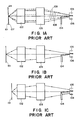
- Figs. 1A - 1C illustrate a principle of a prior art focus detector which uses a knife edge, a light beam reflected by a disk 101 as an information record medium is directed to photo-sensing planes 105 - 106 of a two-split sensor by an objective lens 102 and a sensor lens 103.
- a knife edge 104 is inserted in a light path of the reflected light beam and it is positioned such that light amounts arriving on the photo-sensing planes 105 and 106 are equal in an in-focus state as shown in Fig. 1A.
- the disk is moved away from the in-focus position as shown in Fig.
- the above object of the present invention is achieved by arranging an optical element which serves to split a portion of a detected light beam only when an irradiated light beam is not in an in-focus state on an object surface, in a vicinity of a focus point of the detected light beam which is formed by focusing the light beam irradiated to the object surface and reflected thereby or transmitted therethrough.
- Fig. 2 shows a first embodiment of the focus detector of the present invention applied to an optical disk apparatus.
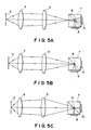
- a light emitted from a light source 1 such as a semiconductor laser is collimated by a collimater lens 2, passes through a beam splitter 3 and is focused by an objective lens 4 onto a rotating disk 5 which is an object to be tested.
- the light beam reflected by the disk 5 passes through the objective lens 4 and is reflected by the beam splitter 3 and again focused by a sensor lens 6 to form a detection light beam.
- An optical element 7 which comprises junction of triangular prisms and has a stripe-shaped reflection area 8 formed on a portion of the junction plane is arranged in a light path near a focus point of the detection light beam.
- a sensor 9 which senses the detection light beam reflected by the reflection area 8 is arranged on one surface of an outer periphery of the optical element 7, and a sensor 10 which senses a portion of the detection light beam which is not reflected by the reflection area 8 but separated is provided on the other surface.
- Fig. 3 shows a side view of the optical element 7 as viewed in Z direction.
- the reflection area 8 is of stripe shape having a predetermined width so that it totally reflects the detection beam flux and directs it to the sensor 9 when the irradiated light beam is in the in-focus state on the disk 5 as shown in Fig. 2.
- the stripe-shaped reflection area 8 thus has a width corresponding to a light beam diameter (beam waist) at the focus point.
- the optical element 7 is arranged such that the y-axis thereof is parallel to a longitudinal direction of a track on the disk 5.
- a longitudinal direction of the stripe-shaped reflection area 8 corresponds to an orthogonal direction to the track.
- the sensor 9 has a photo-sensing plane thereof split to sections 9a and 9b by a split line parallel to the longitudinal direction of the track as shown in Fig. 4A.
- Signals produced by the photo-sensing planes 9a and 9b are finitely differentiated by a subtractor D1 so that a tracking signal indicating a positional deviation of the irradiated light beam from the track is produced at a terminal C1 by a well-known tracking signal detection principle (so-called push-pull method).
- the outputs of the photo-sensing planes 9a and 9b are summed by an adder A1 and a sum signal is produced at a terminal C2.
- the senor 10 has a photo-sensing plane thereof split into three sections 10a, 10b and 10c by two split lines parallel to the normal line to the track as shown in Fig. 4B.
- the signals of the photo-sensing planes 10a and 10c are summed in an adder A2 and a sum signal and the output signal of the photo-sensing plane 10b are finitely differentiated by a subtractor D2 so that a focus error signal is produced at a terminal C3.
- the output of the adder A2 and the photo-sensing plane 10b are summed by an adder A3 and a sum signal is produced at a terminal C4.
- a sum of the outputs at the terminals C2 and C4 represents a total light intensity of the detection light beam, and a reproduced RF signal corresponding to the information recorded on the disk 5 is produced by adding those signals.
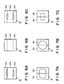
- Figs. 6A - 6C and Figs. 7A -7C show light distributions on the sensors 10 and 9 corresponding to the states shown in Figs. 5A - 5C, respectively.
- the detection light beam is directed to the reflection area 8 at the focus point and totally reflected thereby and sensed only by the sensor 9 as shown in Fig. 7B. Accordingly, as shown in Fig. 6B, the light does not reach the sensor 10 and no output in produced at the terminal C3 of Fig. 4B.
- the focus point of the detection light beam moves forward and the detection light beam overflows from the reflection area 8 and a portion thereof is split and detected by the sensor 10.
- a portion of an arcuate spot is directed to the photo-sensing plane of the sensor 10 as shown in Fig. 6A.
- the focus point of the detection light beam moves backward and the detection light beam again overflows from the reflection area 8 and a portion thereof is split and directed to the sensor 10. Since the light intensity of the photo-sensing planes 10a and 10c is smaller than the light intensity of the photo-sensing plane 10b as opposed to the case of Fig. 5A, a negative focus error signal is produced at the terminal C3 of Fig. 4B. The magnitude of the focus error signal represents the defocus amount of the disk 5 from the in-focus position.
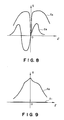
- Figs. 8 and 9 show signal outputs of the sensors 10 and 9, respectively, S1, S2, S3 and S4 show outputs at the terminals C1, C2, C3 and C4 of Figs. 4A and 4B, respectively.
- An abscissa represent the defocus amount ⁇ of the disk 5 from the in-focus position and an ordinate represents the magnitude S of the signal output.
- the focus error signal S3 representing the direction and magnitude of defocusing is produced at the terminal C3.
- the tracking signal S1 is always zero irrespective of ⁇ so that the tracking detection is not affected by the defocusing.
- the focus error signal is not affected by the inclination of the disk 5.
- the detection light beam is not applied to the sensor 10 and no malfunction occurs because the reflection area 8 is located at the focus point.
- the focus error signal is also not affected by the shift of the light beam when the tracking objective lens 4 is moved in the x direction or by the change of light intensity distribution in the detection light beam.
- the reflection area 8 is of stripe shape, a positional accuracy of the optical element 7 in the x direction need not be very high and the optical adjustment can be attained by moving the optical element 7 only in the y direction.
- the reflection area 8 is located at the focus point of the detection light beam.
- the reflection area 81 may be located at other than the focus point in the vicinity of the focus point if the width of the reflection area 81 is selected somewhat wider so that the shift of the light beam does not affect to the focus error signal.
- the reflection area 81 must be located between a front focus point and a rear focus point of the detection light beam when the defocusing is along the optical axis.
- the like elements to those shown in Fig. 5A are designated by the like numerals and detailed explanation thereof is omitted.
- Fig. 12 shows a modification of the sensor in the first embodiment.
- the sensor 10 in Fig. 2 may be replaced by two sensors 12 and 13 each having the photo-sensing plane thereof spit into the sections 12a and 12b, and 13a and 13b.
- the outputs from the respective photo-sensing planes are applied to adders A4, A5 and A6 and a subtracter D3 as shown and a focus error signal and a light intensity signal are produced at terminals C5 and C6, respectively, by the same principle as that of the previous embodiment.
- the present embodiment is effective when it is difficult to manufacture a large size sensor, or when a manufacturing precision of the reflection area 8 is not sufficient to prevent leakage of the light so that a gohst light is created between the sensors 12 and 13.
- the sensor 10 of Fig. 2 may be replaced by sensors 14 and 15 shown in Fig. 13 in which a split line of photo-sensing planes 14a and 14b and a split line of photo-sensing planes 15a and 15b are not parallel but are angled to each other.
- the outputs from the respective photo-sensing planes are supplied to adders A7, A8 and A9 and a subtractor D4 as shown, and a focus error signal and a light intensity signal are produced at terminals C7 and C8 by the same principle as that of the previous embodiment.
- adders A7, A8 and A9 and a subtractor D4 as shown
- a ratio of light beam split can be controlled by moving the sensors 14 and 15 in the x direction because the spacing between the split lines of the photo-sensing planes varies along the x direction.
- the manufacturing error of the optical element can be compensated in the adjustment stage of the optical system.
- the sensors 9 and 10, 12 and 13 or 14 and 15 may be integrated with the optical element 7 or they may be bonded to the outer peripheral surfaces of the optical element 7.
- the reflection area of the optical element 7 need not be of stripe shape but it may be a divided reflection area so that a split line thereof is displaced with regard to the center portion of incident light beam as shown by hatched area 82 of Fig. 14. In this case, the optical adjustment is easy because only one of the two split light beam spots shown in Fig. 6A is created.
- the reflection area need not be of stripe shape but it may be of circle having a predetermined area as shown by a hatched area 83 of Fig. 15. In this case, the focus error signal is produced in the same manner as that of the previous embodiment.
- Fig. 16 shows a second embodiment of the present invention. While only the detection system is shown in a simplified form, the illumination system may be of the same construction as that of Fig. 2. The like elements to those shown in Fig. 2 are designated by the like numerals and detailed explanation thereof is omitted.
- a transmission type optical element 16 is used in place of the optical element 7.
- the optical element 16 is basically a plate-like member which is made of transparent material such as glass or plastic. It has a stripe-shaped area 162 at the center, which is parallel to the opposing plane 164, and outer areas 161 and 163 thereof are inclined with respect to the plane 164.
- a sensor 18 for sensing a detection light beam which passed through the plane 162 is provided on the back side of the optical element 16.
- Sensors 17 and 19 which sense portions of the detection light beam applied to and refracted by the inclined planes 161 and 163 of the optical element 16 in the defocus state
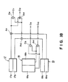
- Fig. 18 shows the photo-sensing planes of the sensors and a signal processing circuit in the present embodiment.
- the sensor 18 has the photo-sensing plane thereof split into two sections 18a and 18b by a split line parallel to the longitudinal direction of the track.
- the signals from the respective photo-sensing planes are summed and subtracted by an adder A10 and a subtractor D5, respectively, so that a light intensity signal and a tracking signal are produced at terminals C10 and C9, respectively.
- the sensors 17 and 19 each has the photo-sensing plane thereof split into two sections 17a and 17b, and 19a and 19b by a split line parallel to a normal line to the track.
- the outputs from the photo-sensing planes 17a and 19a and the outputs from the photo-sensing planes 17b and 19b are summed by address A11 and A12, respectively.
- Sum signals from the address A11 and A12 are summed and subtracted by an adder A13 and a subtractor D6, respectively, so that a focus error signal and a light intensity signal are produced at terminals C11 and C12, respectively.
- a reproduced RF signal is produced by summing the outputs of the terminals C10 and C12.
- Figs. 19A to 19C show detection light beams on the sensor planes in various focus states.
- the principle of the focus detection in the present embodiment is basically identical to that of the first embodiment.
- the detection light beam in the in-focus state, the detection light beam totally passes through a parallel plane 162 of the optical element 16 and is directed only to the sensor 18 as shown in Fig. 19B.
- the stripe-shaped parallel plane 162 has a width corresponding to a beam waist of the detection light beam.
- the detection light beam overflows from the plane 162 of the optical element 16, is refracted by the inclined planes 161 and 163 so that a portion of the light beam is split and it is sensed by the sensors 17 and 19 as shown in Fig. 19A.
- the light intensities of the photo-sensing planes 17b and 19b are larger than the light intensities of the photo-sensing planes 17a and 19a so that a positive focus error signal is produced at a terminal C11 of Fig. 18.
- the detection light beam is split by the optical element 16 and directed to the sensors 17 and 19 as shown in Fig. 19C.
- the light intensities of the photo-sensing planes 17a and 19a are larger than the light intensities of the photo-sensing planes 17b and 19b, and a negative focus error signal is produced at the terminal C11 of Fig. 18.
- the focus error signal is detected without affecting to the tracking signal, as is done in the first embodiment.
- the present embodiment is similar to the first embodiment in that a malfunction due to the inclination of the disk is hard to occur.
- Fig. 20 shows a third embodiment of the present invention. While only the detection system is shown in a simplified form, the illumination system may be identical to that of Fig. 2. The like elements to those shown in Fig. 2 are designated by the like numerals and detailed description thereof may be omitted.
- a transmission type optical element 20 is used in place of the optical element 7 of Fig. 2.
- the optical element 20 is basically a plate-like member made of transparent material such as glass or plastic.
- One plane of the optical element 20 is split into a plane 201 which is parallel to the other plane 203 and a plane 202 which is inclined with respect to the plane 203.
- the optical element 20 is arranged in a light path of the detection light beam so that the split line is spaced from an optical axis by a distance d.
- a sensor 21 for sensing the detection light beam which passed through the plane 201 and a sensor 22 which senses a portion of the detection light beam refracted by the inclined plane 202 in the defocus state are arranged on the back side of the optical element 20.
- Fig. 22 shows the photo-sensing planes of the sensors and a signal processing circuit in the present embodiment.
- the sensor 21 has the photo-sensing plane thereof split into two sections 21a and 21b by a split line parallel to the longitudinal direction of the track.
- the signals from the respective photo-sensing planes are summed and subtracted by an adder A14 and a subtractor D7, respectively, so that a light intensity signal and a tracking signal are produced at terminals C14 and C13, respectively.
- the sensor 22 has the photo-sensing plane thereof split into two sections 22a and 22b by a split line parallel to a normal line to the track.
- the outputs of the photo-sensing planes 22a and 22b are summed and subtracted by an adder A15 and a subtractor D6 so that a focus error signal and a light intensity signal are produced at terminals C16 and C15, respectively.
- a reproduced RF signal is produced by summing the outputs of the terminals C14 and C15.
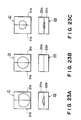
- Figs. 23A to 23C show the detection light beams on the sensor planes in various focus states.
- the principle of the focus detection in the present embodiment is basically identical to that of the first embodiment.
- the detection light beam in the in-focus state, the detection light beam totally passes through the parallel plane 201 of the optical element 20 and is directed to only the sensor 21 as shown in Fig. 23B.
- no focus error signal is produced.
- the detection light beam overflows from the plane 201 of the optical element 20, is refracted by the inclined plane 202 and a portion thereof is split and sensed by the sensor 22 as shown in Fig. 23A.
- the light intensity of the photo-sensing plane 22a is larger than the light intensity of the photo-sensing plane 22b so that a positive focus error signal is produced at the terminal C16 of Fig. 22.
- the detection light beam is split by the optical element 20 and directed to the sensor 22 as shown in Fig. 23C.
- the light intensity of the photo-sensing plane 22b is larger than the light intensity of the photo-sensing plane 22a so that a negative focus error signal is produced at the terminal C16 of Fig. 22.
- the present embodiment offers the same advantages as those which the first embodiment does.
- Fig. 24 shows a fourth embodiment of the focus detector of the present invention applied to an optical disk.
- the like elements to those shown in Fig. 2 are designated by the like numerals and detailed explanation thereof is omitted.
- a diffraction grating 23 is arranged in a light path of an illumination light beam so that it splits the light beam into three beams to form three spots on the disk 5.
- the spots are irradiated such that the center spot is directed to the center of the track on the disk 5 and the spots at the opposite ends are halfly directed to the opposite sides of the track.
- the light reflected by the center spot is sensed by the sensors 26 and 27 to detect the reproduced RF signal and the focusing signal, and the lights reflected by the opposite end spots are sensed by the sensors 25 and 28 to produce the tracking signal by a well-known three-beam method.
- the optical element 24 which is identical to the optical element 20 of the third embodiment is arranged in the light path of the reflected light beam, and three light beams L1, L2 and L3 corresponding to the three spots are directed to the optical element 24 as shown in Fig. 25.
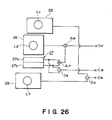
- Fig. 26 shows the photo-sensing planes of the sensors and a signal processing circuit in the present embodiment.
- the light beams L1, L2 and L3 are sensed by the sensors 25, 26 and 28, respectively.
- the sensor 27 senses a portion of the light beam L2 split by the optical element 24 in the defocus state.
- the principle of detection of the focus error signal from the light beam L2 is same as that in the third embodiment and the explanation thereof is omitted.
- the outputs of the split photo-sensing planes 27a and 27b of the sensor 27 are differentiated by a subtractor D9 so that the focus error signal is produced at the terminal C16.
- the outputs from the photo-sensing planes 27a and 27b are summed by an adder A17 and a sum signal is added to the output of the sensor 26 by an adder A16 so that a reproduced RF signal is produced at the terminal C17.
- the outputs of the sensors 25 and 28 are finitely differentiated by a subtractor D10 by the three-beam method so that the tracking signal is produced at the terminal C19.
- a half-mirror may be provided in a light path of the detection light beam and a light beam split thereby may be sensed by a separate sensor to produce the reproduced RF signal.
- the focus error signal may be produced by a light beam which passed through the object.
- the present invention is applicable to not only the disk apparatus but also other optical information recording and reproducing apparatus and an optical instrument such as a shape detector or range finder.
Landscapes
- Physics & Mathematics (AREA)
- Optics & Photonics (AREA)
- General Physics & Mathematics (AREA)
- Optical Recording Or Reproduction (AREA)
- Automatic Focus Adjustment (AREA)
Applications Claiming Priority (2)
| Application Number | Priority Date | Filing Date | Title |
|---|---|---|---|
| JP61210031A JPH0734264B2 (ja) | 1986-09-05 | 1986-09-05 | 光学式情報記録再生装置 |
| JP210031/86 | 1986-09-05 |
Publications (3)
| Publication Number | Publication Date |
|---|---|
| EP0259148A2 true EP0259148A2 (de) | 1988-03-09 |
| EP0259148A3 EP0259148A3 (en) | 1988-11-30 |
| EP0259148B1 EP0259148B1 (de) | 1992-01-29 |
Family
ID=16582663
Family Applications (1)
| Application Number | Title | Priority Date | Filing Date |
|---|---|---|---|
| EP87307745A Expired - Lifetime EP0259148B1 (de) | 1986-09-05 | 1987-09-02 | Fokusdetektor |
Country Status (3)
| Country | Link |
|---|---|
| EP (1) | EP0259148B1 (de) |
| JP (1) | JPH0734264B2 (de) |
| DE (1) | DE3776467D1 (de) |
Cited By (7)
| Publication number | Priority date | Publication date | Assignee | Title |
|---|---|---|---|---|
| EP0405507A3 (en) * | 1989-06-28 | 1991-12-27 | Dainippon Screen Mfg. Co., Ltd. | Displacement detection system |
| GB2248989A (en) * | 1990-10-15 | 1992-04-22 | Applied Magnetics Corp | Focus detection |
| US5245174A (en) * | 1990-10-15 | 1993-09-14 | Applied Magnetics Corporation | Focus sensing apparatus utilizing a reflecting surface having variable reflectivity |
| EP1150286A3 (de) * | 2000-04-20 | 2002-09-18 | Seiko Instruments Inc. | Optischer Nahfeldkopf |
| CN103018733A (zh) * | 2012-12-18 | 2013-04-03 | 山东省科学院海洋仪器仪表研究所 | 一种天文望远镜焦点定位装置 |
| CN104198163A (zh) * | 2014-09-19 | 2014-12-10 | 南京信息工程大学 | 望远镜焦点精确定位的装置 |
| CN107003112A (zh) * | 2014-12-17 | 2017-08-01 | 科磊股份有限公司 | 用于半导体检验及计量的线扫描刀口高度传感器 |
Families Citing this family (1)
| Publication number | Priority date | Publication date | Assignee | Title |
|---|---|---|---|---|
| DE10300843A1 (de) * | 2003-01-10 | 2004-07-22 | Deutsche Thomson-Brandt Gmbh | Gerät zum Lesen und/oder Beschreiben optischer Aufzeichnungsträger |
Family Cites Families (4)
| Publication number | Priority date | Publication date | Assignee | Title |
|---|---|---|---|---|
| FR2325953A1 (fr) * | 1975-09-29 | 1977-04-22 | Thomson Brandt | Senseur optique de focalisation et dispositif de focalisation comportant un tel senseur |
| NL8104588A (nl) * | 1981-10-08 | 1983-05-02 | Philips Nv | Bundelscheidingsprisma, werkwijze voor het vervaardigen van dit prisma en van dit prisma voorziene optische lees- en/of schrijfeenheid. |
| NL8202058A (nl) * | 1982-05-19 | 1983-12-16 | Philips Nv | Opto-elektronisch fokusfout-detektiestelsel. |
| JPS61168135A (ja) * | 1985-01-18 | 1986-07-29 | Seiko Instr & Electronics Ltd | 光情報検出装置 |
-
1986
- 1986-09-05 JP JP61210031A patent/JPH0734264B2/ja not_active Expired - Fee Related
-
1987
- 1987-09-02 EP EP87307745A patent/EP0259148B1/de not_active Expired - Lifetime
- 1987-09-02 DE DE8787307745T patent/DE3776467D1/de not_active Expired - Lifetime
Cited By (14)
| Publication number | Priority date | Publication date | Assignee | Title |
|---|---|---|---|---|
| EP0405507A3 (en) * | 1989-06-28 | 1991-12-27 | Dainippon Screen Mfg. Co., Ltd. | Displacement detection system |
| GB2248989A (en) * | 1990-10-15 | 1992-04-22 | Applied Magnetics Corp | Focus detection |
| US5245174A (en) * | 1990-10-15 | 1993-09-14 | Applied Magnetics Corporation | Focus sensing apparatus utilizing a reflecting surface having variable reflectivity |
| US5349175A (en) * | 1990-10-15 | 1994-09-20 | Applied Magnetics Corporation | Focus sensing apparatus using electrical AGC to enhance differential focus error signal |
| GB2248989B (en) * | 1990-10-15 | 1995-05-24 | Applied Magnetics Corp | Focus sensing apparatus and method |
| EP1150286A3 (de) * | 2000-04-20 | 2002-09-18 | Seiko Instruments Inc. | Optischer Nahfeldkopf |
| US6744708B2 (en) | 2000-04-20 | 2004-06-01 | Seiko Instruments Inc. | Near-field optical head |
| CN103018733A (zh) * | 2012-12-18 | 2013-04-03 | 山东省科学院海洋仪器仪表研究所 | 一种天文望远镜焦点定位装置 |
| CN104198163A (zh) * | 2014-09-19 | 2014-12-10 | 南京信息工程大学 | 望远镜焦点精确定位的装置 |
| CN107003112A (zh) * | 2014-12-17 | 2017-08-01 | 科磊股份有限公司 | 用于半导体检验及计量的线扫描刀口高度传感器 |
| KR20170096001A (ko) * | 2014-12-17 | 2017-08-23 | 케이엘에이-텐코 코포레이션 | 반도체 검사 및 계측을 위한 라인 주사 나이프 에지 높이 센서 |
| EP3234990A4 (de) * | 2014-12-17 | 2018-08-08 | KLA - Tencor Corporation | Zeilenabtastender messerkantenhöhensensor für halbleiterinspektion und messtechnik |
| CN114719765A (zh) * | 2014-12-17 | 2022-07-08 | 科磊股份有限公司 | 用于半导体检验及计量的线扫描刀口高度传感器 |
| CN114719765B (zh) * | 2014-12-17 | 2024-12-20 | 科磊股份有限公司 | 用于半导体检验及计量的线扫描刀口高度传感器 |
Also Published As
| Publication number | Publication date |
|---|---|
| EP0259148A3 (en) | 1988-11-30 |
| DE3776467D1 (de) | 1992-03-12 |
| JPS6364636A (ja) | 1988-03-23 |
| EP0259148B1 (de) | 1992-01-29 |
| JPH0734264B2 (ja) | 1995-04-12 |
Similar Documents
| Publication | Publication Date | Title |
|---|---|---|
| US4533826A (en) | Opto-electronic focusing-error detection device | |
| US4712205A (en) | Opto-electronic focussing-error detection system with a compound wedge beam splitter | |
| EP0219908B1 (de) | Gerät zur optischen Abtastung einer Informationsebene | |
| US4815060A (en) | Optical pickup device with tracking and focusing utilizing a photodetector having four regions | |
| JPS618744A (ja) | 光デイスク装置のフオ−カス誤差検出装置 | |
| US5231621A (en) | Focus detector which serves to split off a portion of a detected light beam only when the detected light beam is not refocused at an expected refocus point | |
| EP0259148B1 (de) | Fokusdetektor | |
| US6314063B1 (en) | Integrated light emitting and receiving device and optical pick-up with same | |
| US5287338A (en) | Error signal generation for light beam reflected from optical disk with plurality of light detecting elements | |
| EP0273422A2 (de) | Verfahren und Gerät zur Erfassung von Ausrichtungs- und Fokusfehlern in einem optischen Kopf | |
| EP0336737A2 (de) | Optisches Informationswiedergabegerät | |
| JPS6329337B2 (de) | ||
| JPS5984352A (ja) | 焦点誤差検出装置 | |
| JP2865087B2 (ja) | ランドグルーブ位置検出方式及び方法 | |
| JPS6142743A (ja) | 光学的情報読取装置 | |
| KR0186153B1 (ko) | 광픽업장치 | |
| EP1067532B1 (de) | Optische Abtasteinheit und optisches Plattengerät | |
| JP2596993B2 (ja) | 光ディスクの情報読取方法 | |
| JP2695909B2 (ja) | 光学的情報記録再生装置 | |
| JP2870236B2 (ja) | 光学式記録再生装置 | |
| KR940022435A (ko) | 광 픽업 시스템 | |
| JPS6040534A (ja) | トラツキング制御方法及び装置 | |
| JPS5856235A (ja) | 光学的トラツク追跡装置 | |
| JPH01258233A (ja) | フォーカス制御信号検出方式 | |
| JPS63184931A (ja) | 対物レンズ位置検出装置 |
Legal Events
| Date | Code | Title | Description |
|---|---|---|---|
| PUAI | Public reference made under article 153(3) epc to a published international application that has entered the european phase |
Free format text: ORIGINAL CODE: 0009012 |
|
| AK | Designated contracting states |
Kind code of ref document: A2 Designated state(s): DE FR GB IT NL |
|
| PUAL | Search report despatched |
Free format text: ORIGINAL CODE: 0009013 |
|
| AK | Designated contracting states |
Kind code of ref document: A3 Designated state(s): DE FR GB IT NL |
|
| 17P | Request for examination filed |
Effective date: 19890419 |
|
| 17Q | First examination report despatched |
Effective date: 19900711 |
|
| GRAA | (expected) grant |
Free format text: ORIGINAL CODE: 0009210 |
|
| AK | Designated contracting states |
Kind code of ref document: B1 Designated state(s): DE FR GB IT NL |
|
| REF | Corresponds to: |
Ref document number: 3776467 Country of ref document: DE Date of ref document: 19920312 |
|
| ITF | It: translation for a ep patent filed | ||
| ET | Fr: translation filed | ||
| PLBE | No opposition filed within time limit |
Free format text: ORIGINAL CODE: 0009261 |
|
| STAA | Information on the status of an ep patent application or granted ep patent |
Free format text: STATUS: NO OPPOSITION FILED WITHIN TIME LIMIT |
|
| 26N | No opposition filed | ||
| ITTA | It: last paid annual fee | ||
| REG | Reference to a national code |
Ref country code: GB Ref legal event code: IF02 |
|
| PGFP | Annual fee paid to national office [announced via postgrant information from national office to epo] |
Ref country code: DE Payment date: 20030919 Year of fee payment: 17 |
|
| PGFP | Annual fee paid to national office [announced via postgrant information from national office to epo] |
Ref country code: GB Payment date: 20040819 Year of fee payment: 18 |
|
| PGFP | Annual fee paid to national office [announced via postgrant information from national office to epo] |
Ref country code: NL Payment date: 20040923 Year of fee payment: 18 |
|
| PGFP | Annual fee paid to national office [announced via postgrant information from national office to epo] |
Ref country code: FR Payment date: 20040927 Year of fee payment: 18 |
|
| PG25 | Lapsed in a contracting state [announced via postgrant information from national office to epo] |
Ref country code: DE Free format text: LAPSE BECAUSE OF NON-PAYMENT OF DUE FEES Effective date: 20050401 |
|
| PG25 | Lapsed in a contracting state [announced via postgrant information from national office to epo] |
Ref country code: IT Free format text: LAPSE BECAUSE OF NON-PAYMENT OF DUE FEES;WARNING: LAPSES OF ITALIAN PATENTS WITH EFFECTIVE DATE BEFORE 2007 MAY HAVE OCCURRED AT ANY TIME BEFORE 2007. THE CORRECT EFFECTIVE DATE MAY BE DIFFERENT FROM THE ONE RECORDED. Effective date: 20050902 Ref country code: GB Free format text: LAPSE BECAUSE OF NON-PAYMENT OF DUE FEES Effective date: 20050902 |
|
| PG25 | Lapsed in a contracting state [announced via postgrant information from national office to epo] |
Ref country code: NL Free format text: LAPSE BECAUSE OF NON-PAYMENT OF DUE FEES Effective date: 20060401 |
|
| GBPC | Gb: european patent ceased through non-payment of renewal fee |
Effective date: 20050902 |
|
| PG25 | Lapsed in a contracting state [announced via postgrant information from national office to epo] |
Ref country code: FR Free format text: LAPSE BECAUSE OF NON-PAYMENT OF DUE FEES Effective date: 20060531 |
|
| NLV4 | Nl: lapsed or anulled due to non-payment of the annual fee |
Effective date: 20060401 |
|
| REG | Reference to a national code |
Ref country code: FR Ref legal event code: ST Effective date: 20060531 |