EP0259613A1 - Procédé de fabrication de dispositifs à couches imprégnées - Google Patents
Procédé de fabrication de dispositifs à couches imprégnées Download PDFInfo
- Publication number
- EP0259613A1 EP0259613A1 EP87111356A EP87111356A EP0259613A1 EP 0259613 A1 EP0259613 A1 EP 0259613A1 EP 87111356 A EP87111356 A EP 87111356A EP 87111356 A EP87111356 A EP 87111356A EP 0259613 A1 EP0259613 A1 EP 0259613A1
- Authority
- EP
- European Patent Office
- Prior art keywords
- contacts
- impregnation
- ceramic
- metal
- impregnating material
- Prior art date
- Legal status (The legal status is an assumption and is not a legal conclusion. Google has not performed a legal analysis and makes no representation as to the accuracy of the status listed.)
- Granted
Links
Images
Classifications
-
- H—ELECTRICITY
- H01—ELECTRIC ELEMENTS
- H01G—CAPACITORS; CAPACITORS, RECTIFIERS, DETECTORS, SWITCHING DEVICES, LIGHT-SENSITIVE OR TEMPERATURE-SENSITIVE DEVICES OF THE ELECTROLYTIC TYPE
- H01G4/00—Fixed capacitors; Processes of their manufacture
- H01G4/002—Details
- H01G4/228—Terminals
- H01G4/232—Terminals electrically connecting two or more layers of a stacked or rolled capacitor
- H01G4/2325—Terminals electrically connecting two or more layers of a stacked or rolled capacitor characterised by the material of the terminals
-
- H—ELECTRICITY
- H01—ELECTRIC ELEMENTS
- H01G—CAPACITORS; CAPACITORS, RECTIFIERS, DETECTORS, SWITCHING DEVICES, LIGHT-SENSITIVE OR TEMPERATURE-SENSITIVE DEVICES OF THE ELECTROLYTIC TYPE
- H01G4/00—Fixed capacitors; Processes of their manufacture
- H01G4/30—Stacked capacitors
- H01G4/302—Stacked capacitors obtained by injection of metal in cavities formed in a ceramic body
-
- H—ELECTRICITY
- H05—ELECTRIC TECHNIQUES NOT OTHERWISE PROVIDED FOR
- H05K—PRINTED CIRCUITS; CASINGS OR CONSTRUCTIONAL DETAILS OF ELECTRIC APPARATUS; MANUFACTURE OF ASSEMBLAGES OF ELECTRICAL COMPONENTS
- H05K3/00—Apparatus or processes for manufacturing printed circuits
- H05K3/10—Apparatus or processes for manufacturing printed circuits in which conductive material is applied to the insulating support in such a manner as to form the desired conductive pattern
- H05K3/101—Apparatus or processes for manufacturing printed circuits in which conductive material is applied to the insulating support in such a manner as to form the desired conductive pattern by casting or moulding of conductive material
-
- H—ELECTRICITY
- H05—ELECTRIC TECHNIQUES NOT OTHERWISE PROVIDED FOR
- H05K—PRINTED CIRCUITS; CASINGS OR CONSTRUCTIONAL DETAILS OF ELECTRIC APPARATUS; MANUFACTURE OF ASSEMBLAGES OF ELECTRICAL COMPONENTS
- H05K3/00—Apparatus or processes for manufacturing printed circuits
- H05K3/40—Forming printed elements for providing electric connections to or between printed circuits
- H05K3/403—Edge contacts; Windows or holes in the substrate having plural connections on the walls thereof
Definitions
- the invention relates to a method for producing filler layer components from monolithic ceramics by impregnating a ceramic layer structure from dense and porous layers with a liquid impregnation material and by applying contacts.
- Sintered ceramic bodies with porous and dense layers can e.g. according to DE-PS 24 62 006, DE-PS 24 62 008 or DE-PS 24 45 087.
- Such partially porous ceramic parts are then provided, for example according to DE-PS 22 18 170 or DE-PS 22 64 943, with electrically conductive metal fillings, with different process technologies being available.
- electrically conductive metal fillings with different process technologies being available.
- Known among other things is the impregnation with silver nitrate solution with subsequent decomposition of the silver nitrate at a higher temperature with formation of a precipitate or also an impregnation with silver nitrate solution with subsequent reduction of the silver nitrate with hydrogen at a higher temperature to the metallic silver.
- liquid metals or alloys for example bismuth (Bi) -, lead (Pb) -, aluminum (Al) -, copper (Cu) -, zinc (Zn) -, tin (Sn) - has also proven its worth. or also cadmium (Cd) alloys.
- contacts For the intended use of the components, contacts must be applied to the ceramic, which guarantee an electrical connection to the metal filling and thus enable further processing to, for example, capacitors in SMD construction.
- the contacts for the application of the contacts, for example, the baking of noble metal pastes or metal coating processes via the gas phase can be considered.
- DE-AS 23 23 921 therefore describes in particular the application of a porous, sintered glass boundary layer to the end faces of the ceramic body, which is intended to hinder the liquid material from leaking out after the actual impregnation process. After impregnation, this glass boundary layer must be removed in a separate process step, after which the contacts are subsequently applied.
- the object of the invention is to simplify the production of filler layer components, in particular ceramic capacitors, by pressure impregnation of porous ceramic parts.
- the object is achieved in that the contacts are applied after the impregnation process without further intermediate steps and that the contacts are electrically connected to the metal filling.
- Pb-In alloys have proven their worth as impregnation materials, but Cu-In or Ag-In alloys and other materials are also conceivable. If the alloys PbAg5In5, PbIn2.5 or PbIn5 are used as the impregnation material, due to the wetting effect of the indium, the metal filling does not leak when the ceramic parts are removed from the impregnation bath and the parts remain completely filled. Possibly adhering impregnation material on the outer surfaces of the ceramic parts is removed if necessary by a chemical aftertreatment. After the impregnation process, the contacts and the electrical connection between the metal filling and the contacts can then be applied in any manner.
- the contacts can also be applied by known surface coating processes, for example vapor deposition or sputtering. If necessary, these can be galvanically reinforced and, if necessary, connected by heat treatment above the melting temperature of the impregnation material.
- the melting temperature of the impregnation material is to be regarded as the upper operating temperature of capacitors produced in this way, since changes in the electrical characteristic data can result from repeated melting of the metal filling.
- the melting points of the impregnation materials should preferably be above the melting temperature of conventional solder baths, which are used when the components are used as intended.
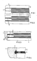
- FIG. 1 and 2 show a detail from a component 1 which has a layer structure of dense and porous layers 2.
- capacitors can be realized on the basis of the dielectric properties of the ceramic.
- the porous layers 2 must be filled with an impregnating metal in a suitable manner. The latter is done, for example, by pressure or centrifugal drinkers, for which lead-based materials are used, for example.
- the outer surfaces of the ceramic component 1 have hitherto been coated with fine-porous coatings, for example by sintering on glass frits, which had to be removed mechanically after the pressure impregnation.
- the firing of silver pastes as contacts as a preliminary step is also known, by means of which a pressure impregnation is possible. In any case, additional effort was necessary.
- FIG. 2 shows the same ceramic component 1 as FIG. 1 with an alloy wetting the ceramic in the liquid state. It can be seen that the areas 2 are completely filled with impregnation material, so that in this case contacts 3 can subsequently be applied and electrically connected to the metal filling.
- FIGS. 3 and 4 The electrical connection of metal filling 5 and contacts 3 is clear from FIGS. 3 and 4. It can be seen that in heat treatments due to the temperature-related volume expansion and due to the phase transition solid-liquid impregnation material of the metal filling 5 emerges from the areas 2 of the ceramic to be contacted. The heat treatment advantageously takes place below the melting point of the contacts, but above the melting temperature of the impregnation material. The connection of the contacts to the metal filling is achieved in the areas 6.
- Cavity ceramic parts should be soaked with PbIn5.
- a process temperature of 420 ° C. is selected and soaked in an autoclave at 10 bar for 30 seconds.
- the contacts are then applied by dipping in precious metal paste and then baking.
- the electrical connection takes place simultaneously with this heat treatment, which can be, for example, 60 minutes at 550 ° C. in an air atmosphere.
- the heating and cooling rate during the heat treatment was 15 K / min. chosen.
- PbAg5In5 is chosen as the impregnation material, with the process temperature between 350 and 500 ° C and the pressure between 5 and 10 bar.
- the contacts can be produced according to Example 1 or Example 2.
- Cavity ceramic parts are soaked according to Example 1 or Example 3. Then the outer sides with NiCr / Ag and then with the desired layer sequence, e.g. NiCr / Ag / Ni / Sn finished by sputtering or electrodeposition. A separate temperature treatment after the sputtering process according to Example 2 has no adverse effects on the required electrical properties.
Landscapes
- Engineering & Computer Science (AREA)
- Power Engineering (AREA)
- Manufacturing & Machinery (AREA)
- Microelectronics & Electronic Packaging (AREA)
- Chemical & Material Sciences (AREA)
- Ceramic Engineering (AREA)
- Fixed Capacitors And Capacitor Manufacturing Machines (AREA)
- Ceramic Capacitors (AREA)
- Powder Metallurgy (AREA)
- Manufacture Of Alloys Or Alloy Compounds (AREA)
- Cell Electrode Carriers And Collectors (AREA)
- Manufacturing Of Electrical Connectors (AREA)
- Basic Packing Technique (AREA)
Priority Applications (1)
| Application Number | Priority Date | Filing Date | Title |
|---|---|---|---|
| AT87111356T ATE66088T1 (de) | 1986-08-18 | 1987-08-05 | Verfahren zur herstellung von fuellschichtbauteilen. |
Applications Claiming Priority (2)
| Application Number | Priority Date | Filing Date | Title |
|---|---|---|---|
| DE3627936 | 1986-08-18 | ||
| DE3627936 | 1986-08-18 |
Publications (2)
| Publication Number | Publication Date |
|---|---|
| EP0259613A1 true EP0259613A1 (fr) | 1988-03-16 |
| EP0259613B1 EP0259613B1 (fr) | 1991-08-07 |
Family
ID=6307608
Family Applications (1)
| Application Number | Title | Priority Date | Filing Date |
|---|---|---|---|
| EP87111356A Expired - Lifetime EP0259613B1 (fr) | 1986-08-18 | 1987-08-05 | Procédé de fabrication de dispositifs à couches imprégnées |
Country Status (6)
| Country | Link |
|---|---|
| US (1) | US4913932A (fr) |
| EP (1) | EP0259613B1 (fr) |
| JP (1) | JPS6352406A (fr) |
| AT (1) | ATE66088T1 (fr) |
| DE (1) | DE3771973D1 (fr) |
| ES (1) | ES2023384B3 (fr) |
Families Citing this family (7)
| Publication number | Priority date | Publication date | Assignee | Title |
|---|---|---|---|---|
| JPH03125027U (fr) * | 1990-03-27 | 1991-12-18 | ||
| JPH06737A (ja) * | 1991-03-29 | 1994-01-11 | Shin Etsu Chem Co Ltd | 静電チャック基板 |
| US5239744A (en) * | 1992-01-09 | 1993-08-31 | At&T Bell Laboratories | Method for making multilayer magnetic components |
| US5456088A (en) * | 1993-11-12 | 1995-10-10 | Thermo King Corporation | Refrigeration unit and method of operating same |
| US5879812A (en) * | 1995-06-06 | 1999-03-09 | Murata Manufacturing Co., Ltd. | Monolithic ceramic capacitor and method of producing the same |
| JP5796568B2 (ja) * | 2012-02-03 | 2015-10-21 | 株式会社村田製作所 | セラミック電子部品 |
| US11443898B2 (en) | 2017-04-10 | 2022-09-13 | Presidio Components. Inc. | Multilayer broadband ceramic capacitor with internal air gap capacitance |
Citations (2)
| Publication number | Priority date | Publication date | Assignee | Title |
|---|---|---|---|---|
| US3679950A (en) * | 1971-04-16 | 1972-07-25 | Nl Industries Inc | Ceramic capacitors |
| US4071880A (en) * | 1974-06-10 | 1978-01-31 | N L Industries, Inc. | Ceramic bodies with end termination electrodes |
Family Cites Families (13)
| Publication number | Priority date | Publication date | Assignee | Title |
|---|---|---|---|---|
| CA566871A (fr) * | 1958-12-02 | L. Schnable George | Methode de placage chimique de metaux | |
| US4030004A (en) * | 1971-04-16 | 1977-06-14 | Nl Industries, Inc. | Dielectric ceramic matrices with end barriers |
| US3829356A (en) * | 1971-04-16 | 1974-08-13 | Nl Industries Inc | Sintered ceramic bodies with porous portions |
| US3772748A (en) * | 1971-04-16 | 1973-11-20 | Nl Industries Inc | Method for forming electrodes and conductors |
| US3965552A (en) * | 1972-07-24 | 1976-06-29 | N L Industries, Inc. | Process for forming internal conductors and electrodes |
| DE2462006C3 (de) * | 1973-09-24 | 1978-06-22 | Nl Industries, Inc., New York, N.Y. (V.St.A.) | Mehrschichtige Schaltkreisstrukturmatrix und Verfahren zu ihrer Herstellung |
| DE2462008C3 (de) * | 1973-09-24 | 1979-09-13 | Nl Industries, Inc., New York, N.Y. (V.St.A.) | Mehrschichtige Schaltkreisstruktur und Verfahren zu ihrer Herstellung |
| US4353957A (en) * | 1973-09-24 | 1982-10-12 | Tam Ceramics Inc. | Ceramic matrices for electronic devices and process for forming same |
| US3879645A (en) * | 1973-09-24 | 1975-04-22 | Nl Industries Inc | Ceramic capacitors |
| US4019168A (en) * | 1975-08-21 | 1977-04-19 | Airco, Inc. | Bilayer thin film resistor and method for manufacture |
| JPS53267A (en) * | 1976-06-23 | 1978-01-05 | Kubota Ltd | Process for enlarging pipe diameter |
| US4430690A (en) * | 1982-10-07 | 1984-02-07 | International Business Machines Corporation | Low inductance MLC capacitor with metal impregnation and solder bar contact |
| US4584629A (en) * | 1984-07-23 | 1986-04-22 | Avx Corporation | Method of making ceramic capacitor and resulting article |
-
1987
- 1987-08-05 DE DE8787111356T patent/DE3771973D1/de not_active Expired - Lifetime
- 1987-08-05 AT AT87111356T patent/ATE66088T1/de active
- 1987-08-05 ES ES87111356T patent/ES2023384B3/es not_active Expired - Lifetime
- 1987-08-05 EP EP87111356A patent/EP0259613B1/fr not_active Expired - Lifetime
- 1987-08-14 JP JP62203002A patent/JPS6352406A/ja active Pending
- 1987-08-18 US US07/086,520 patent/US4913932A/en not_active Expired - Fee Related
Patent Citations (2)
| Publication number | Priority date | Publication date | Assignee | Title |
|---|---|---|---|---|
| US3679950A (en) * | 1971-04-16 | 1972-07-25 | Nl Industries Inc | Ceramic capacitors |
| US4071880A (en) * | 1974-06-10 | 1978-01-31 | N L Industries, Inc. | Ceramic bodies with end termination electrodes |
Also Published As
| Publication number | Publication date |
|---|---|
| JPS6352406A (ja) | 1988-03-05 |
| DE3771973D1 (de) | 1991-09-12 |
| ES2023384B3 (es) | 1992-01-16 |
| EP0259613B1 (fr) | 1991-08-07 |
| US4913932A (en) | 1990-04-03 |
| ATE66088T1 (de) | 1991-08-15 |
Similar Documents
| Publication | Publication Date | Title |
|---|---|---|
| EP0302274B1 (fr) | Composant électrique multicouche et procédé de fabrication | |
| EP0016307B1 (fr) | Procédé pour fabriquer une structure multicouches en vitrocéramique comportant des conducteurs internes à base de cuivre | |
| DE4021364C2 (fr) | ||
| DE69128218T2 (de) | Festelektrolytkondensator in Chip-Bauweise | |
| DE3509593A1 (de) | Verfahren zur herstellung eines keramikkondensators und danach hergestellter kondensator | |
| DE69022668T2 (de) | Elektronische Verbindungen, Verfahren zur Bildung von Endverbindern dafür und Paste zur Ausbildung derselben. | |
| EP0259613B1 (fr) | Procédé de fabrication de dispositifs à couches imprégnées | |
| DE1558897B2 (de) | Verfahren zum Verbinden von Metallen mit Metallen | |
| DE1907267A1 (de) | Loetbares Teil,insbesondere zur Verwendung als Verschlusselement bei einem Elektrolytkondensator,und Verfahren zu seiner Herstellung | |
| DE3148778C2 (fr) | ||
| DE68912365T2 (de) | Mehrschichtkondensator. | |
| DE3900741A1 (de) | Verfahren zum abschliessen eines bleigefuellten kondensators und danach hergestellter kondensator | |
| EP0258670B1 (fr) | Composant à couches imprégnées | |
| EP0260427A1 (fr) | Composant à couches imprégnées et son procédé de fabrication | |
| EP1774543B1 (fr) | Composant électrique et procédé pour produire un composant électrique | |
| DE4308361C2 (de) | Verfahren zur Herstellung einer Verbindung zweier Keramikteile bzw. eines Metall- und eines Keramikteils | |
| DE3406542A1 (de) | Verfahren zum herstellen eines halbleiterbauelementes | |
| DE1621258B2 (de) | Kontaktstueck aus einem leitenden traeger aus einem unedlen metall und einem dreischichtigen verbundkontaktkoerper sowie dessen herstellungsverfahren | |
| DE2522944C3 (de) | Verfahren zur Herstellung einer elektrischen Dünnfilmschaltung | |
| DE2227238A1 (de) | Glaskoerper, insbesondere glasscheibe, die eine oder mehrere schichten aus metall oder metall und metalloxyd aufweist und verfahren zu ihrer herstellung | |
| DE1564822C (de) | Verfahren zur Herstellung von elektri sehen Kondensatoren mit Halbleiterschicht | |
| DE2347410B2 (de) | Elektrolytkondensator mit einer glashuelle | |
| CH383733A (de) | Verfahren zum Anlöten eines Diamanten an eine Metallfassung | |
| DE2606962A1 (de) | Verfahren zur hartloetfaehigen metallisierung von vorzugsweise oxidkeramischen bauteilen sowie metallisierungspaste zur ausuebung des verfahrens | |
| DE825192C (de) | Verfahren zur Kontaktierung von Halbleiter-Widerstaenden aus Metalloxyden |
Legal Events
| Date | Code | Title | Description |
|---|---|---|---|
| PUAI | Public reference made under article 153(3) epc to a published international application that has entered the european phase |
Free format text: ORIGINAL CODE: 0009012 |
|
| AK | Designated contracting states |
Kind code of ref document: A1 Designated state(s): AT BE CH DE ES FR GB IT LI |
|
| 17P | Request for examination filed |
Effective date: 19880406 |
|
| 17Q | First examination report despatched |
Effective date: 19901109 |
|
| GRAA | (expected) grant |
Free format text: ORIGINAL CODE: 0009210 |
|
| AK | Designated contracting states |
Kind code of ref document: B1 Designated state(s): AT BE CH DE ES FR GB IT LI |
|
| REF | Corresponds to: |
Ref document number: 66088 Country of ref document: AT Date of ref document: 19910815 Kind code of ref document: T |
|
| REF | Corresponds to: |
Ref document number: 3771973 Country of ref document: DE Date of ref document: 19910912 |
|
| ET | Fr: translation filed | ||
| ITF | It: translation for a ep patent filed | ||
| GBT | Gb: translation of ep patent filed (gb section 77(6)(a)/1977) | ||
| REG | Reference to a national code |
Ref country code: ES Ref legal event code: FG2A Ref document number: 2023384 Country of ref document: ES Kind code of ref document: B3 |
|
| PLBE | No opposition filed within time limit |
Free format text: ORIGINAL CODE: 0009261 |
|
| STAA | Information on the status of an ep patent application or granted ep patent |
Free format text: STATUS: NO OPPOSITION FILED WITHIN TIME LIMIT |
|
| PGFP | Annual fee paid to national office [announced via postgrant information from national office to epo] |
Ref country code: GB Payment date: 19920717 Year of fee payment: 6 |
|
| PGFP | Annual fee paid to national office [announced via postgrant information from national office to epo] |
Ref country code: AT Payment date: 19920722 Year of fee payment: 6 |
|
| 26N | No opposition filed | ||
| PGFP | Annual fee paid to national office [announced via postgrant information from national office to epo] |
Ref country code: ES Payment date: 19920811 Year of fee payment: 6 |
|
| PGFP | Annual fee paid to national office [announced via postgrant information from national office to epo] |
Ref country code: BE Payment date: 19920814 Year of fee payment: 6 |
|
| PGFP | Annual fee paid to national office [announced via postgrant information from national office to epo] |
Ref country code: FR Payment date: 19920821 Year of fee payment: 6 |
|
| PGFP | Annual fee paid to national office [announced via postgrant information from national office to epo] |
Ref country code: DE Payment date: 19921023 Year of fee payment: 6 |
|
| PGFP | Annual fee paid to national office [announced via postgrant information from national office to epo] |
Ref country code: CH Payment date: 19921120 Year of fee payment: 6 |
|
| PG25 | Lapsed in a contracting state [announced via postgrant information from national office to epo] |
Ref country code: GB Effective date: 19930805 Ref country code: AT Effective date: 19930805 |
|
| PG25 | Lapsed in a contracting state [announced via postgrant information from national office to epo] |
Ref country code: ES Free format text: LAPSE BECAUSE OF THE APPLICANT RENOUNCES Effective date: 19930806 |
|
| PG25 | Lapsed in a contracting state [announced via postgrant information from national office to epo] |
Ref country code: LI Effective date: 19930831 Ref country code: CH Effective date: 19930831 Ref country code: BE Effective date: 19930831 |
|
| BERE | Be: lapsed |
Owner name: SIEMENS A.G. Effective date: 19930831 |
|
| GBPC | Gb: european patent ceased through non-payment of renewal fee |
Effective date: 19930805 |
|
| PG25 | Lapsed in a contracting state [announced via postgrant information from national office to epo] |
Ref country code: FR Effective date: 19940429 |
|
| REG | Reference to a national code |
Ref country code: CH Ref legal event code: PL |
|
| PG25 | Lapsed in a contracting state [announced via postgrant information from national office to epo] |
Ref country code: DE Effective date: 19940503 |
|
| REG | Reference to a national code |
Ref country code: FR Ref legal event code: ST |
|
| REG | Reference to a national code |
Ref country code: ES Ref legal event code: FD2A Effective date: 19991007 |
|
| PG25 | Lapsed in a contracting state [announced via postgrant information from national office to epo] |
Ref country code: IT Free format text: LAPSE BECAUSE OF NON-PAYMENT OF DUE FEES;WARNING: LAPSES OF ITALIAN PATENTS WITH EFFECTIVE DATE BEFORE 2007 MAY HAVE OCCURRED AT ANY TIME BEFORE 2007. THE CORRECT EFFECTIVE DATE MAY BE DIFFERENT FROM THE ONE RECORDED. Effective date: 20050805 |