EP0259614A1 - Mémoire pour signaux électroniques numériques - Google Patents
Mémoire pour signaux électroniques numériques Download PDFInfo
- Publication number
- EP0259614A1 EP0259614A1 EP87111361A EP87111361A EP0259614A1 EP 0259614 A1 EP0259614 A1 EP 0259614A1 EP 87111361 A EP87111361 A EP 87111361A EP 87111361 A EP87111361 A EP 87111361A EP 0259614 A1 EP0259614 A1 EP 0259614A1
- Authority
- EP
- European Patent Office
- Prior art keywords
- membrane
- memory
- memory according
- substrate
- states
- Prior art date
- Legal status (The legal status is an assumption and is not a legal conclusion. Google has not performed a legal analysis and makes no representation as to the accuracy of the status listed.)
- Granted
Links
Images


Classifications
-
- H—ELECTRICITY
- H01—ELECTRIC ELEMENTS
- H01H—ELECTRIC SWITCHES; RELAYS; SELECTORS; EMERGENCY PROTECTIVE DEVICES
- H01H1/00—Contacts
- H01H1/0036—Switches making use of microelectromechanical systems [MEMS]
-
- G—PHYSICS
- G11—INFORMATION STORAGE
- G11C—STATIC STORES
- G11C11/00—Digital stores characterised by the use of particular electric or magnetic storage elements; Storage elements therefor
- G11C11/21—Digital stores characterised by the use of particular electric or magnetic storage elements; Storage elements therefor using electric elements
- G11C11/24—Digital stores characterised by the use of particular electric or magnetic storage elements; Storage elements therefor using electric elements using capacitors
-
- G—PHYSICS
- G11—INFORMATION STORAGE
- G11C—STATIC STORES
- G11C17/00—Read-only memories programmable only once; Semi-permanent stores, e.g. manually-replaceable information cards
- G11C17/04—Read-only memories programmable only once; Semi-permanent stores, e.g. manually-replaceable information cards using capacitive elements
-
- G—PHYSICS
- G11—INFORMATION STORAGE
- G11C—STATIC STORES
- G11C23/00—Digital stores characterised by movement of mechanical parts to effect storage, e.g. using balls; Storage elements therefor
-
- H—ELECTRICITY
- H01—ELECTRIC ELEMENTS
- H01H—ELECTRIC SWITCHES; RELAYS; SELECTORS; EMERGENCY PROTECTIVE DEVICES
- H01H1/00—Contacts
- H01H1/0036—Switches making use of microelectromechanical systems [MEMS]
- H01H2001/0042—Bistable switches, i.e. having two stable positions requiring only actuating energy for switching between them, e.g. with snap membrane or by permanent magnet
Definitions
- the invention relates to a memory for digital electronic signals with a permanent memory of the type specified in the preamble of claim 1.
- Such memories with memory elements that can be electrically set and reset during operation are required in electronic devices for storing information even after device downtimes.
- Memory elements of this kind have been known for some time, for example in the form of ferrite rings in the ring core memory, in the form of magnetic domains in the magnetic bubble memory, in the form of bistable multivibrators in an R Andom A ccess M emory (RAM) with buffer battery for bridging supply voltage failure or in the form of the operating chargeable and dischargeable capacitors in a "e lectrically e rasable P rogrammable R ead o nly M emory” (EEPROM).
- RAM Random A ccess M emory
- EEPROM e lectrically e rasable P rogrammable R ead o nly M emory
- Memory elements of the type mentioned have the disadvantage that, like the ferrite core memories and magnetic bubble memories, they cannot be produced using the same technology as the control circuits and are therefore slow and expensive, or that, like the semiconductor memories, they only hold the information for a limited time, e.g. B. until the RAM in the battery is exhausted or until the charge from the capacitor one EEPROM memory cell z. B. has flowed under the influence of ionizing radiation.
- the EEPROM memory cell also has a very limited number of write cycles with 104 to 106.
- the invention is based on the object of creating a memory of the type mentioned, the content of which, even over a long period of time, despite external influences such.
- B. ionizing radiation is captive and its dimensions and technology are suitable for integration with transistors on a semiconductor substrate.
- micromechanical and electronic components can be produced on a semiconductor substrate using the same or related methods.
- An integration of at least one of these memory elements according to the invention with the associated electronics on a substrate enables particularly advantageous embodiments of the invention because of the smallness of the memory element, the low power consumption and the methods suitable for mass production.
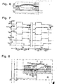
- a storage element 1 consists of a bridge-shaped membrane 2 deformed under mechanical tension, which has two stable positional states 3 and 4, a support 5 and a recess 6 on the surface of an advantageously weakly p-conducting silicon (Si) single crystal wafer, which is called substrate 7 below.
- the production of the memory element 1 initially follows the state of the art according to the Petersen article cited.
- For the generation of the bridge-shaped membrane 2 must locally on the substrate 7 photolithographic masks limit a suitable sequence of layers (FIG. 2) so that the desired mechanical elements can be exposed by etching in the last process step: - Generation of any electronic elements 8, which are arranged under the membrane 2, and their connecting lines.
- a barrier layer 9 is generated on the substrate 7 in the region of the recess 6, which limits the material removal in depth during etching.
- a highly conductive p+-Si layer can be produced by diffusing boron into the substrate surface or by oxidation of the substrate surface, a coating of SiO2 (insulator), for example as a cover for electronic elements 8 or conductor tracks 11.
- SiO2 insulator
- a weakly conductive p-Si layer is built up over this barrier layer 9, the thickness of which determines the height of the supports 5.
- - Outside the areas with underlying barrier layer 9 can, for. B. electronic elements 8 and associated conductor tracks.
- An insulator layer 10 is produced by oxidation of the surface via this layer for the supports 5. It forms a base layer 10 ⁇ for the membranes 2nd - Application of the necessary metallic conductor tracks 11, z. B. from Au, Cr, Al etc.
- a metal layer 12 is deposited on the membranes 2 at temperatures of the substrate 7 in the region of the boiling nitrogen, z. B. 20 to 100 nm thick.
- the metal layer 12 can be constructed from one or more layers, from different metals or alloys, e.g. B. from Al, Cr Au, Fe etc.
- the membranes 2 are etched free.
- the operational electronic-micromechanical circuits are checked like normal IC circuits and z. B. packed in the standardized IC package.
- FIG. 3 shows an exemplary embodiment with the same reference numbers for the same element as in FIGS. 1 and 2.
- a membrane 2 In order for a membrane 2 to be moved from one position 3 or 4 to another position 4 or 3, a mechanical spring force generated by the compression stresses must be overcome until the membrane 2 tilts into the other position 3, 4 under its own spring force .
- the overturning time of the membrane 2 depends on its dimensions. This mechanically bistable behavior of the membrane 2 is used to store the information, the two logic states "0" and "1" being assigned to the position states 3, 4.
- the dimensions of the membranes 2 depend on the advances in IC technology.
- a typical exemplary embodiment in today's technology with a 2 ⁇ m line width has a membrane 2 with the dimensions of 10 ⁇ m length, 2 ⁇ m width and 0.1 ⁇ m thickness.
- the deflection of the membrane 2 is approximately 0.1 ⁇ m in each of the two position states 3, 4.
- the height of the supports 5 measures 0.2 ⁇ m.
- the overturn time is a few microseconds.
- the small mass of the membrane 2 of a few ng prevents a mechanical switching of the membrane 2 by acceleration forces.
- the membrane 2 consists only of the metal layer 12 formed from at least one metal or at least one metal alloy. - Several mutually independent membranes 2 on the same substrate 7 enable more information to be stored accordingly, and - Several membranes 2 bridge the same depression 6 in parallel.
- the barrier layer 9 on the substrate 7 consists of an electrically highly conductive material, e.g. B. p+-Si ( Figure 4).
- the membrane 2 with the metal layer 12 and the barrier layer 9 form a plate capacitor 12 ⁇ , the capacitance value of which is determined by the membrane dimensions, the height of the supports 5 and the position 3, 4 of the membrane 2.
- a control of the capacitor plates is shown by way of example in FIG. 4.
- a memory cell 13 consists of two field effect transistors 14, 15 with an insulated gate 16 (MOSFET) and the memory element 1 shown in section. Another embodiment of the memory cell 1 is characterized by an additional one Shield 17 covering memory cell 1.
- the shield 17 covers at a distance of z. B. 0.1 to 1 mm all of the memory elements 1 located on the same substrate 7 and is conductively connected to the reference potential of all electrically relevant voltages on the substrate 7 formed from the substrate 7 and the substrates 18 of the MOSFET 14, 15 of each memory cell 13.
- a W ORD (W) line 19 connects each GATE 16 of the MOSFET 14, 15 of a memory cell 13 and the GATE 16 of the corresponding MOSFET 14, 15 from any further memory cells 13.
- the current through the MOSFET 14, 15, ie between contacts 20 , 21 and contacts 22, 23 is controlled by means of the potential of the GATE 16.
- the contact 20 of the MOSFET 14 is electrically connected to the membrane 2 or the metal layer 12.
- the other contact 22 of the MOSFET 14 is connected via a B IT B RIDGE (BB) line 24 to contacts 22 of the MOSFET 14 and any other memory cells 13.
- BB B IT B RIDGE
- the contact 21 of the MOSFET 15 is electrically connected to the barrier layer 9 of the memory element 1.
- a B F IT ORCE (BF) line 25 connects contacts 23 of the MOSFET 15 of the memory cells 13.
- the footprint of a memory cell 13 is about ten times of a memory element of a modern U se Dynamic R Andom A ccess memory block.
- FIG. 4 shows an example of a read-out device 26 for querying the positional state 3, 4 by measuring the capacitance value of the plate capacitor 12 ⁇ of a memory cell 13.
- the W line 19 is brought to a potential V DD (z. B. + 5 V).
- the BB line 24 and the BF line 25 are given a duration ⁇ of z. B. ten natural vibrations of the membrane 2 a potential V SP (z. B. + 10 to + 20 V). Since both MOSFETs 14, 15 are electrically conductive, an electrical charge flows into the capacitor formed from the metal layer 12 and the environment (eg shield 17) and into the capacitor formed from the barrier layer 9 and the substrate 7. The charge of the same name in the barrier layer 9 and the metal layer 12 generate a repulsive force acting between the two layers 9, 12. If the membrane 2 is in the position 3, the mechanical forces acting in the membrane 2 are overcome and the membrane 2 snaps into the position 4.
- the potential V SP must be during the Duration ⁇ can be maintained on lines 24, 25 until the natural vibrations of membrane 2 have safely subsided.
- the BB and BF lines 24, 25 are then connected to the reference potential and the electrical charges are removed from the storage element 1.
- the W line 19 can then be connected to the reference potential, ie the MOSFETs 14, 15 isolate the memory element 1 from the electr. Feeders 24, 15.
- the potential V DD is applied to the W line 19 and the BB line 24 is kept at the reference potential.
- the BF line 25 receives the potential V SP for the duration ⁇ , and the plate capacitor 12 ⁇ is charged. The forces therefore acting on the membrane 2 overcome the mechanical forces which hold the membrane 2 in the positional state 4, and the membrane 2 snaps in the positional state 3.
- the W -Line 19 also placed on the reference potential so that the memory element 1 is electrically isolated again.
- a function U W means the potential of the W line 19, a function U BF the potential of the BF line 25 and a function U BB the potential of the BB line as a function of time t.
- U BF and U BB for reaching the state 4 only U BF have the potential V SP for the duration ⁇ , while the W line 19 has the time ⁇ additionally required for discharging at the potential V DD lies.
- a write cycle 27 is therefore composed of the times ⁇ and ⁇ .
- a function P symbolically indicates the position of the membrane 2, which is switched between the two position states 3, 4. In FIG. 5, two write cycles 27 for the position state 4 follow one after the other as an example, and a write cycle 27 for the position state 3 follows later.
- the storage element Use electromagnetic forces to move the membrane 2 from one position to the other.
- the barrier layer 9 and the metal layer 12 are formed in FIG. 6 as conductors guided in parallel.
- One of the two streams 28, 29 can be reversed in the direction by means of these electronic means, e.g. B. instead of the current 28, a current 30 flows in the opposite direction.
- the membrane 2 If the currents 29, 30 flow, ie in the opposite direction to one another, the membrane 2 is pressed into the state 4 by the electromagnetic forces; However, if the currents 28, 29 flow, ie parallel to one another, the membrane 2 is brought into position 3 by the electromagnetic forces.
- the electrically highly conductive barrier layer 9 can also be replaced by an insulating barrier layer made of SiO2 with an underlying well conductive conductor track 11 if this reduces the number of manufacturing steps.
- the time sequence of a read cycle 38 is recorded in FIG.
- the elements 19, 24, 25 and 31 to 37 are shown in FIG. 4 and used in the description for FIG. 7 with the same reference numbers.
- the read cycle 38 consists of a PRECHARGE phase 39 and a SENSE phase 40.
- a function S37 shows the position of the switch 37, the function U BB the potential of the BB line 24, a function U35 the potential in point 35, the function U W is the potential of the W line 19 and a function A is the signal at the output 34.
- the reading cycle 38 begins with the PRECHARGE phase 39.
- the capacitor 31 is discharged via the changeover switch 36.
- the PRECHARGE phase ends when the switch 37 is switched off and the point 35 is switched to the potential V DD .
- a charge flows from the capacitor 31 Q31 ⁇ 1/2 V DD . CD (2) to the BB line 24. Since the potential U W rises to the value V DD at the same time, the MOSFETs 14, 15 (FIG. 4) conduct a charge depending on the state 3, 4 Q3 ⁇ 1/2 V DD . C3 or Q4 ⁇ 1/2 V DD . C4 (3) in the plate capacitor 12 ⁇ .
- Equations 2 and 3 apply only on the condition that the value CS of the stray capacitance 32 is much larger than the sum of the capacitances C3 + C4 + CD.
- the ratio (C3 - C4) / CS is z. B. about 0.02 and ⁇ U BB therefore about 0.01 . V DD .
- known SENSE amplifiers 33 can reliably determine these voltage differences and generate the signal A corresponding to the state of the memory element 1 at the output 34.
- the SENSE phase 40 ends with the lowering of U BB to the reference potential, and after a waiting time for the discharge of the plate capacitor 12 ⁇ , the W line 19 is also connected to the reference potential and thus the barrier layer 8 and the metal layer 12 from the lines 24, 25 isolated.
- a memory element 1 with the membrane 2 in the state 3 is read out.
- the larger capacity value C3 compared to CD causes U BB to drop below 1/2 V DD .
- the smaller capacitance value C4 compared to CD leaves 40 ⁇ U BB by ⁇ U BB over 1/2 in the SENSE phase .
- V DD rise.
- the signal A is set to V DD as soon as the SENSE amplifier 33 detects the increase in U BB .
- Memory cells 13 in the above-mentioned embodiments can be arranged individually or in large numbers on a substrate 7.
- the stores Cells 13 are organized BIT-wise or BYTE-wise, as is usual with RAM, EEPROM etc., and can be controlled by address lines.
- the organization of the memory cells can be done by the display e.g. B. be determined as a dot matrix.
Landscapes
- Engineering & Computer Science (AREA)
- Physics & Mathematics (AREA)
- Electromagnetism (AREA)
- Power Engineering (AREA)
- Computer Hardware Design (AREA)
- Semiconductor Memories (AREA)
- Signal Processing For Digital Recording And Reproducing (AREA)
- Semiconductor Integrated Circuits (AREA)
- Measuring Fluid Pressure (AREA)
- Credit Cards Or The Like (AREA)
Priority Applications (1)
| Application Number | Priority Date | Filing Date | Title |
|---|---|---|---|
| AT87111361T ATE72075T1 (de) | 1986-09-10 | 1987-08-06 | Speicher fuer digitale elektronische signale. |
Applications Claiming Priority (2)
| Application Number | Priority Date | Filing Date | Title |
|---|---|---|---|
| CH3647/86A CH670914A5 (fr) | 1986-09-10 | 1986-09-10 | |
| CH3647/86 | 1986-09-10 |
Publications (2)
| Publication Number | Publication Date |
|---|---|
| EP0259614A1 true EP0259614A1 (fr) | 1988-03-16 |
| EP0259614B1 EP0259614B1 (fr) | 1992-01-22 |
Family
ID=4260485
Family Applications (1)
| Application Number | Title | Priority Date | Filing Date |
|---|---|---|---|
| EP87111361A Expired - Lifetime EP0259614B1 (fr) | 1986-09-10 | 1987-08-06 | Mémoire pour signaux électroniques numériques |
Country Status (8)
| Country | Link |
|---|---|
| US (1) | US4979149A (fr) |
| EP (1) | EP0259614B1 (fr) |
| JP (1) | JPS6373554A (fr) |
| AT (1) | ATE72075T1 (fr) |
| CH (1) | CH670914A5 (fr) |
| DE (1) | DE3776237D1 (fr) |
| GR (1) | GR3004073T3 (fr) |
| NO (1) | NO873761L (fr) |
Cited By (7)
| Publication number | Priority date | Publication date | Assignee | Title |
|---|---|---|---|---|
| WO1994027308A1 (fr) * | 1993-05-06 | 1994-11-24 | Cavendish Kinetics Limited | Element memoire bistable |
| EP0758128A1 (fr) * | 1995-08-09 | 1997-02-12 | Siemens Aktiengesellschaft | Dispositif de mémoire et procédé de fabrication |
| WO1997029538A1 (fr) * | 1996-02-10 | 1997-08-14 | Fraunhofer-Gesellschaft zur Förderung der angewandten Forschung e.V. | Microactionneur bistable a membranes couplees |
| US6100109A (en) * | 1994-11-02 | 2000-08-08 | Siemens Aktiengesellschaft | Method for producing a memory device |
| EP1001440A3 (fr) * | 1998-11-13 | 2002-09-18 | General Electric Company | Structure d'interrupteur et méthode de fabrication |
| WO2006094038A3 (fr) * | 2005-03-02 | 2006-12-21 | Northrop Grumman Corp | Transistor a resonateur en nanotube de carbone, procede de fabrication de ce dernier |
| EP1936680A3 (fr) * | 2006-12-21 | 2008-07-09 | Commissariat A L'energie Atomique | Elément d'interconnexiion à Base de nanotubes de carbone |
Families Citing this family (95)
| Publication number | Priority date | Publication date | Assignee | Title |
|---|---|---|---|---|
| US5538753A (en) * | 1991-10-14 | 1996-07-23 | Landis & Gyr Betriebs Ag | Security element |
| EP0537439B2 (fr) * | 1991-10-14 | 2003-07-09 | OVD Kinegram AG | Elément de sécurité |
| US5638946A (en) * | 1996-01-11 | 1997-06-17 | Northeastern University | Micromechanical switch with insulated switch contact |
| US6237590B1 (en) | 1997-09-18 | 2001-05-29 | Delsys Pharmaceutical Corporation | Dry powder delivery system apparatus |
| US6525483B1 (en) * | 1998-12-22 | 2003-02-25 | Koninklijke Philips Electronics N.V. | Display device comprising a light guide with electrode voltages dependent on previously applied electrode voltages |
| US6211580B1 (en) * | 1998-12-29 | 2001-04-03 | Honeywell International Inc. | Twin configuration for increased life time in touch mode electrostatic actuators |
| US6054745A (en) * | 1999-01-04 | 2000-04-25 | International Business Machines Corporation | Nonvolatile memory cell using microelectromechanical device |
| AU2565800A (en) * | 1999-03-18 | 2000-10-04 | Cavendish Kinetics Limited | Flash memory cell having a flexible element |
| WO2001003208A1 (fr) * | 1999-07-02 | 2001-01-11 | President And Fellows Of Harvard College | Dispositifs s nanoscopiques a base de fils, ensembles ainsi formes et procedes de fabrication y relatifs |
| JP2001102597A (ja) | 1999-09-30 | 2001-04-13 | Fuji Electric Co Ltd | 半導体構造およびその製造方法 |
| US6716657B1 (en) * | 2000-05-26 | 2004-04-06 | Agere Systems Inc | Method for interconnecting arrays of micromechanical devices |
| US6473361B1 (en) | 2000-11-10 | 2002-10-29 | Xerox Corporation | Electromechanical memory cell |
| US6924538B2 (en) | 2001-07-25 | 2005-08-02 | Nantero, Inc. | Devices having vertically-disposed nanofabric articles and methods of making the same |
| US6574130B2 (en) * | 2001-07-25 | 2003-06-03 | Nantero, Inc. | Hybrid circuit having nanotube electromechanical memory |
| US6919592B2 (en) | 2001-07-25 | 2005-07-19 | Nantero, Inc. | Electromechanical memory array using nanotube ribbons and method for making same |
| US6911682B2 (en) * | 2001-12-28 | 2005-06-28 | Nantero, Inc. | Electromechanical three-trace junction devices |
| US7259410B2 (en) | 2001-07-25 | 2007-08-21 | Nantero, Inc. | Devices having horizontally-disposed nanofabric articles and methods of making the same |
| US6706402B2 (en) | 2001-07-25 | 2004-03-16 | Nantero, Inc. | Nanotube films and articles |
| US7563711B1 (en) * | 2001-07-25 | 2009-07-21 | Nantero, Inc. | Method of forming a carbon nanotube-based contact to semiconductor |
| US7566478B2 (en) | 2001-07-25 | 2009-07-28 | Nantero, Inc. | Methods of making carbon nanotube films, layers, fabrics, ribbons, elements and articles |
| US6835591B2 (en) | 2001-07-25 | 2004-12-28 | Nantero, Inc. | Methods of nanotube films and articles |
| US6643165B2 (en) | 2001-07-25 | 2003-11-04 | Nantero, Inc. | Electromechanical memory having cell selection circuitry constructed with nanotube technology |
| US6784028B2 (en) | 2001-12-28 | 2004-08-31 | Nantero, Inc. | Methods of making electromechanical three-trace junction devices |
| US7176505B2 (en) | 2001-12-28 | 2007-02-13 | Nantero, Inc. | Electromechanical three-trace junction devices |
| US20060182389A1 (en) * | 2002-03-26 | 2006-08-17 | Duine Peter A | Display device comprising a light transmitting first plate and light-absorbing means |
| US7335395B2 (en) | 2002-04-23 | 2008-02-26 | Nantero, Inc. | Methods of using pre-formed nanotubes to make carbon nanotube films, layers, fabrics, ribbons, elements and articles |
| JP4186727B2 (ja) * | 2002-07-26 | 2008-11-26 | 松下電器産業株式会社 | スイッチ |
| CN100490044C (zh) * | 2002-07-26 | 2009-05-20 | 松下电器产业株式会社 | 开关 |
| US6972881B1 (en) | 2002-11-21 | 2005-12-06 | Nuelight Corp. | Micro-electro-mechanical switch (MEMS) display panel with on-glass column multiplexers using MEMS as mux elements |
| US7560136B2 (en) | 2003-01-13 | 2009-07-14 | Nantero, Inc. | Methods of using thin metal layers to make carbon nanotube films, layers, fabrics, ribbons, elements and articles |
| FR2852441A1 (fr) * | 2003-03-14 | 2004-09-17 | St Microelectronics Sa | Dispositif de memoire |
| EP1631812A4 (fr) | 2003-05-14 | 2010-12-01 | Nantero Inc | Plateforme de detection faisant appel a un element a nanotubes a orientation horizontale |
| US7199498B2 (en) | 2003-06-02 | 2007-04-03 | Ambient Systems, Inc. | Electrical assemblies using molecular-scale electrically conductive and mechanically flexible beams and methods for application of same |
| US7274064B2 (en) | 2003-06-09 | 2007-09-25 | Nanatero, Inc. | Non-volatile electromechanical field effect devices and circuits using same and methods of forming same |
| US7280394B2 (en) | 2003-06-09 | 2007-10-09 | Nantero, Inc. | Field effect devices having a drain controlled via a nanotube switching element |
| FR2858459B1 (fr) * | 2003-08-01 | 2006-03-10 | Commissariat Energie Atomique | Commutateur micro-mecanique bistable, methode d'actionnement et procede de realisation correspondant |
| WO2005017967A2 (fr) * | 2003-08-13 | 2005-02-24 | Nantero, Inc. | Structure dispositif a nanotube et son procede de production |
| US7289357B2 (en) * | 2003-08-13 | 2007-10-30 | Nantero, Inc. | Isolation structure for deflectable nanotube elements |
| WO2005048296A2 (fr) | 2003-08-13 | 2005-05-26 | Nantero, Inc. | Elements de commutation a base de nanotubes comprenant des commandes multiples et circuits produits a partir de ces elements |
| WO2005084164A2 (fr) * | 2003-08-13 | 2005-09-15 | Nantero, Inc. | Circuits logiques et element de commutation fondes sur des nanotubes |
| US7115960B2 (en) * | 2003-08-13 | 2006-10-03 | Nantero, Inc. | Nanotube-based switching elements |
| US7416993B2 (en) * | 2003-09-08 | 2008-08-26 | Nantero, Inc. | Patterned nanowire articles on a substrate and methods of making the same |
| US7215229B2 (en) * | 2003-09-17 | 2007-05-08 | Schneider Electric Industries Sas | Laminated relays with multiple flexible contacts |
| JP4626142B2 (ja) * | 2003-11-18 | 2011-02-02 | 株式会社日立製作所 | 装置およびそれを用いたデータ処理方法 |
| US7528437B2 (en) * | 2004-02-11 | 2009-05-05 | Nantero, Inc. | EEPROMS using carbon nanotubes for cell storage |
| CA2568140A1 (fr) * | 2004-05-24 | 2006-07-20 | Trustees Of Boston University | Element memoire nanochimique commandable |
| US7709880B2 (en) * | 2004-06-09 | 2010-05-04 | Nantero, Inc. | Field effect devices having a gate controlled via a nanotube switching element |
| US7164744B2 (en) * | 2004-06-18 | 2007-01-16 | Nantero, Inc. | Nanotube-based logic driver circuits |
| US7330709B2 (en) * | 2004-06-18 | 2008-02-12 | Nantero, Inc. | Receiver circuit using nanotube-based switches and logic |
| US7167026B2 (en) * | 2004-06-18 | 2007-01-23 | Nantero, Inc. | Tri-state circuit using nanotube switching elements |
| US7288970B2 (en) | 2004-06-18 | 2007-10-30 | Nantero, Inc. | Integrated nanotube and field effect switching device |
| US7161403B2 (en) | 2004-06-18 | 2007-01-09 | Nantero, Inc. | Storage elements using nanotube switching elements |
| US7329931B2 (en) * | 2004-06-18 | 2008-02-12 | Nantero, Inc. | Receiver circuit using nanotube-based switches and transistors |
| WO2007024204A2 (fr) * | 2004-07-19 | 2007-03-01 | Ambient Systems, Inc. | Moteurs et generateurs electrostatiques et electromagnetiques nanometriques |
| WO2006121461A2 (fr) | 2004-09-16 | 2006-11-16 | Nantero, Inc. | Photoemetteurs a nanotubes et procedes de fabrication |
| EP1792149B1 (fr) | 2004-09-22 | 2010-03-31 | Nantero, Inc. | Memoire vive comprenant des elements de commutation a nanotube |
| WO2006040726A1 (fr) * | 2004-10-15 | 2006-04-20 | Koninklijke Philips Electronics N.V. | Procede d'exploitation d'un systeme rfid |
| US7046539B1 (en) | 2004-11-02 | 2006-05-16 | Sandia Corporation | Mechanical memory |
| US7598544B2 (en) * | 2005-01-14 | 2009-10-06 | Nanotero, Inc. | Hybrid carbon nanotude FET(CNFET)-FET static RAM (SRAM) and method of making same |
| US8362525B2 (en) | 2005-01-14 | 2013-01-29 | Nantero Inc. | Field effect device having a channel of nanofabric and methods of making same |
| US9911743B2 (en) | 2005-05-09 | 2018-03-06 | Nantero, Inc. | Nonvolatile nanotube diodes and nonvolatile nanotube blocks and systems using same and methods of making same |
| US7479654B2 (en) | 2005-05-09 | 2009-01-20 | Nantero, Inc. | Memory arrays using nanotube articles with reprogrammable resistance |
| US9196615B2 (en) | 2005-05-09 | 2015-11-24 | Nantero Inc. | Nonvolatile nanotube diodes and nonvolatile nanotube blocks and systems using same and methods of making same |
| US8013363B2 (en) * | 2005-05-09 | 2011-09-06 | Nantero, Inc. | Nonvolatile nanotube diodes and nonvolatile nanotube blocks and systems using same and methods of making same |
| US7835170B2 (en) | 2005-05-09 | 2010-11-16 | Nantero, Inc. | Memory elements and cross point switches and arrays of same using nonvolatile nanotube blocks |
| TWI324773B (en) | 2005-05-09 | 2010-05-11 | Nantero Inc | Non-volatile shadow latch using a nanotube switch |
| US7394687B2 (en) * | 2005-05-09 | 2008-07-01 | Nantero, Inc. | Non-volatile-shadow latch using a nanotube switch |
| US8217490B2 (en) | 2005-05-09 | 2012-07-10 | Nantero Inc. | Nonvolatile nanotube diodes and nonvolatile nanotube blocks and systems using same and methods of making same |
| US7781862B2 (en) | 2005-05-09 | 2010-08-24 | Nantero, Inc. | Two-terminal nanotube devices and systems and methods of making same |
| US8513768B2 (en) | 2005-05-09 | 2013-08-20 | Nantero Inc. | Nonvolatile nanotube diodes and nonvolatile nanotube blocks and systems using same and methods of making same |
| US7782650B2 (en) * | 2005-05-09 | 2010-08-24 | Nantero, Inc. | Nonvolatile nanotube diodes and nonvolatile nanotube blocks and systems using same and methods of making same |
| US7928521B1 (en) | 2005-05-31 | 2011-04-19 | Nantero, Inc. | Non-tensioned carbon nanotube switch design and process for making same |
| US7915122B2 (en) * | 2005-06-08 | 2011-03-29 | Nantero, Inc. | Self-aligned cell integration scheme |
| JP5054936B2 (ja) * | 2005-06-22 | 2012-10-24 | パナソニック株式会社 | 電気機械メモリ、それを用いた電気回路及び電気機械メモリの駆動方法 |
| US7349236B2 (en) * | 2005-06-24 | 2008-03-25 | Xerox Corporation | Electromechanical memory cell with torsional movement |
| US7538040B2 (en) * | 2005-06-30 | 2009-05-26 | Nantero, Inc. | Techniques for precision pattern transfer of carbon nanotubes from photo mask to wafers |
| GB0515980D0 (en) * | 2005-08-03 | 2005-09-07 | Cavendish Kinetics Ltd | Memory cell for a circuit and method of operation therefor |
| AU2006287641B2 (en) | 2005-09-06 | 2010-11-11 | Nantero, Inc. | Carbon nanotube resonators |
| US8553455B2 (en) * | 2005-09-27 | 2013-10-08 | Cornell Research Foundation, Inc. | Shape memory device |
| GB0525025D0 (en) * | 2005-12-08 | 2006-01-18 | Cavendish Kinetics Ltd | memory Cell and Array |
| US7336527B1 (en) * | 2005-12-14 | 2008-02-26 | International Business Machines Corporation | Electromechanical storage device |
| KR100827705B1 (ko) * | 2006-10-23 | 2008-05-07 | 삼성전자주식회사 | 비 휘발성 메모리 소자 및 그의 제조방법 |
| KR100834829B1 (ko) * | 2006-12-19 | 2008-06-03 | 삼성전자주식회사 | 멀티 비트 전기 기계적 메모리 소자 및 그의 제조방법 |
| WO2008124084A2 (fr) | 2007-04-03 | 2008-10-16 | Pinkerton Joseph F | Systèmes nano-électromécaniques et procédés de fabrication de ceux-ci |
| US8031514B2 (en) | 2007-04-09 | 2011-10-04 | Northeastern University | Bistable nanoswitch |
| JP5026144B2 (ja) * | 2007-05-18 | 2012-09-12 | 日本電信電話株式会社 | 記憶素子 |
| TWI461350B (zh) * | 2007-05-22 | 2014-11-21 | Nantero Inc | 使用奈米結構物之三極管及其製造方法 |
| WO2009002748A1 (fr) * | 2007-06-22 | 2008-12-31 | Nantero, Inc. | Dispositifs à nanotubes à deux bornes comprenant un pont de nanotubes et procédés de fabrication de ces dispositifs |
| US8704314B2 (en) * | 2007-12-06 | 2014-04-22 | Massachusetts Institute Of Technology | Mechanical memory transistor |
| US9263126B1 (en) | 2010-09-01 | 2016-02-16 | Nantero Inc. | Method for dynamically accessing and programming resistive change element arrays |
| US8253171B1 (en) | 2009-08-27 | 2012-08-28 | Lockheed Martin Corporation | Two terminal nanotube switch, memory array incorporating the same and method of making |
| US20130113810A1 (en) * | 2011-11-04 | 2013-05-09 | Qualcomm Mems Technologies, Inc. | Sidewall spacers along conductive lines |
| ITTO20120224A1 (it) | 2012-03-15 | 2013-09-16 | St Microelectronics Srl | Elemento di memoria elettromeccanico integrato e memoria elettronica comprendente il medesimo |
| KR101928344B1 (ko) * | 2012-10-24 | 2018-12-13 | 삼성전자주식회사 | 나노 공진 장치 및 방법 |
| FR3085786B1 (fr) * | 2018-09-11 | 2021-02-19 | Commissariat Energie Atomique | Cellule de memorisation en logique capacitive |
Citations (4)
| Publication number | Priority date | Publication date | Assignee | Title |
|---|---|---|---|---|
| FR2357023A1 (fr) * | 1976-06-30 | 1978-01-27 | Ibm | Dispositif d'affichage par deformation de membrane et son procede de fabrication |
| FR2376549A1 (fr) * | 1977-01-04 | 1978-07-28 | Thomson Csf | Systeme bistable a electrets |
| EP0046873A1 (fr) * | 1980-09-02 | 1982-03-10 | Texas Instruments Incorporated | Modulateur de lumière à miroir déformable |
| WO1986003879A1 (fr) * | 1984-12-19 | 1986-07-03 | Simpson George R | Dispositifs electrostatiques de commutation binaire et de memoire |
Family Cites Families (8)
| Publication number | Priority date | Publication date | Assignee | Title |
|---|---|---|---|---|
| US4113360A (en) * | 1977-03-28 | 1978-09-12 | Siemens Aktiengesellschaft | Indicating device for illustrating symbols of all kinds |
| US4229732A (en) * | 1978-12-11 | 1980-10-21 | International Business Machines Corporation | Micromechanical display logic and array |
| US4441791A (en) * | 1980-09-02 | 1984-04-10 | Texas Instruments Incorporated | Deformable mirror light modulator |
| US4356730A (en) * | 1981-01-08 | 1982-11-02 | International Business Machines Corporation | Electrostatically deformographic switches |
| US4543457A (en) * | 1984-01-25 | 1985-09-24 | Transensory Devices, Inc. | Microminiature force-sensitive switch |
| US4736202A (en) * | 1984-08-21 | 1988-04-05 | Bos-Knox, Ltd. | Electrostatic binary switching and memory devices |
| US4704707A (en) * | 1984-08-21 | 1987-11-03 | Bos-Knox, Ltd. | Electrostatic random access memory |
| US4570139A (en) * | 1984-12-14 | 1986-02-11 | Eaton Corporation | Thin-film magnetically operated micromechanical electric switching device |
-
1986
- 1986-09-10 CH CH3647/86A patent/CH670914A5/de not_active IP Right Cessation
-
1987
- 1987-08-06 AT AT87111361T patent/ATE72075T1/de not_active IP Right Cessation
- 1987-08-06 EP EP87111361A patent/EP0259614B1/fr not_active Expired - Lifetime
- 1987-08-06 DE DE8787111361T patent/DE3776237D1/de not_active Expired - Fee Related
- 1987-09-02 JP JP62218110A patent/JPS6373554A/ja active Pending
- 1987-09-09 NO NO873761A patent/NO873761L/no unknown
-
1989
- 1989-10-05 US US07/417,338 patent/US4979149A/en not_active Expired - Fee Related
-
1992
- 1992-03-18 GR GR920400471T patent/GR3004073T3/el unknown
Patent Citations (4)
| Publication number | Priority date | Publication date | Assignee | Title |
|---|---|---|---|---|
| FR2357023A1 (fr) * | 1976-06-30 | 1978-01-27 | Ibm | Dispositif d'affichage par deformation de membrane et son procede de fabrication |
| FR2376549A1 (fr) * | 1977-01-04 | 1978-07-28 | Thomson Csf | Systeme bistable a electrets |
| EP0046873A1 (fr) * | 1980-09-02 | 1982-03-10 | Texas Instruments Incorporated | Modulateur de lumière à miroir déformable |
| WO1986003879A1 (fr) * | 1984-12-19 | 1986-07-03 | Simpson George R | Dispositifs electrostatiques de commutation binaire et de memoire |
Non-Patent Citations (3)
| Title |
|---|
| IBM JOURNAL OF RESEARCH AND DEVELOPMENT, Band 23, Nr. 4, Juli 1979, Seiten 376-385, IBM Corp., New York, US; K.E. PETERSEN: "Micromechanical membrane switches on silicon" * |
| IBM TECHNICAL DISCLOSURE BULLETIN, Band 20, Nr. 12, Mai 1978, Seite 5309, New York, US; K.E. PETERSEN: "Bistable micromechanical storage element in silicon" * |
| R.C.A. REVIEW, Band 34, März 1973, Seiten 45-79, Princeton, US; L.S. COSENTINO et al.: "A membrane page composer" * |
Cited By (10)
| Publication number | Priority date | Publication date | Assignee | Title |
|---|---|---|---|---|
| WO1994027308A1 (fr) * | 1993-05-06 | 1994-11-24 | Cavendish Kinetics Limited | Element memoire bistable |
| US6100109A (en) * | 1994-11-02 | 2000-08-08 | Siemens Aktiengesellschaft | Method for producing a memory device |
| EP0758128A1 (fr) * | 1995-08-09 | 1997-02-12 | Siemens Aktiengesellschaft | Dispositif de mémoire et procédé de fabrication |
| US5774414A (en) * | 1995-08-09 | 1998-06-30 | Siemens Aktiengesellschaft | Memory device and production method |
| KR100417481B1 (ko) * | 1995-08-09 | 2004-06-04 | 지멘스 악티엔게젤샤프트 | 메모리장치및그제조방법 |
| WO1997029538A1 (fr) * | 1996-02-10 | 1997-08-14 | Fraunhofer-Gesellschaft zur Förderung der angewandten Forschung e.V. | Microactionneur bistable a membranes couplees |
| EP1001440A3 (fr) * | 1998-11-13 | 2002-09-18 | General Electric Company | Structure d'interrupteur et méthode de fabrication |
| WO2006094038A3 (fr) * | 2005-03-02 | 2006-12-21 | Northrop Grumman Corp | Transistor a resonateur en nanotube de carbone, procede de fabrication de ce dernier |
| US7579618B2 (en) | 2005-03-02 | 2009-08-25 | Northrop Grumman Corporation | Carbon nanotube resonator transistor and method of making same |
| EP1936680A3 (fr) * | 2006-12-21 | 2008-07-09 | Commissariat A L'energie Atomique | Elément d'interconnexiion à Base de nanotubes de carbone |
Also Published As
| Publication number | Publication date |
|---|---|
| GR3004073T3 (fr) | 1993-03-31 |
| JPS6373554A (ja) | 1988-04-04 |
| EP0259614B1 (fr) | 1992-01-22 |
| NO873761L (no) | 1988-03-11 |
| CH670914A5 (fr) | 1989-07-14 |
| DE3776237D1 (de) | 1992-03-05 |
| NO873761D0 (no) | 1987-09-09 |
| ATE72075T1 (de) | 1992-02-15 |
| US4979149A (en) | 1990-12-18 |
Similar Documents
| Publication | Publication Date | Title |
|---|---|---|
| EP0259614B1 (fr) | Mémoire pour signaux électroniques numériques | |
| AT405109B (de) | Ein-elektron speicherbauelement | |
| DE69232389T2 (de) | Informationsverarbeitungsgerät und Rastertunnelmikroskop | |
| DE60025152T2 (de) | MRAM Speicher mit Differenzleseverstärkern | |
| DE60131036T2 (de) | Ein NOT-Schaltkreis | |
| DE69810270T2 (de) | Differentielle flash-speicherzelle und betriebsverfahren dafür | |
| DE69028777T2 (de) | Mikrohergestellte mikroskopeinheit | |
| DE2525225C2 (de) | Lese-Differentialverstärker für durch elektrische Ladungen dargestellte Bits speichernde Halbleiterspeicher | |
| JPH0745794A (ja) | 強誘電体メモリの駆動方法 | |
| DE3513034C2 (de) | Verfahren zur Herstellung einer Halbleitervorrichtung | |
| DE69525637T2 (de) | Speichervorrichtung | |
| DE102009026462A1 (de) | Beschleunigungssensor | |
| DE69524112T2 (de) | Massenspeicherverwendung von lokalprobeanordnung | |
| EP0619494B1 (fr) | Accéléromètre à effet tunnel | |
| DE19621994C1 (de) | Einzelelektron-Speicherzellenanordnung | |
| DE60215161T2 (de) | Feldemissionsvorrichtung zur Erzeugung eines fokussierten Elektronenstrahls | |
| EP0758128B1 (fr) | Dispositif de mémoire et procédé de fabrication | |
| DE2001471B2 (de) | Bitorientierte speicheranordnung und verfahren zur vermeidung des einschreibens von informationen in nur ueber eine zeilenleitung angesteuerte speicherzellen einer bitorientierten speicheranordnung | |
| DE2523683C2 (de) | Integrierte Schaltung mit einer Leitung zum Transport von Ladungen zwischen Speicherelementen eines Halbleiterspeichers und einer Schreib-Lese-Schaltung | |
| DE10393702B4 (de) | Verfahren zum Herstellen einer Speicherzelle, Speicherzelle und Speicherzellen-Anordnung | |
| DE102006004247B4 (de) | Konzept zum Testen einer integrierten Schaltungsanordnung | |
| EP1449220B1 (fr) | Cellule memoire magnetoresistive a couche de reference dynamique | |
| EP0045403A1 (fr) | Méthode de production de cellules de memoire MOS pour réduire l'influence d'irradiation | |
| DE102006004218B3 (de) | Elektromechanische Speicher-Einrichtung und Verfahren zum Herstellen einer elektromechanischen Speicher-Einrichtung | |
| DE19746138A1 (de) | Verfahren zum Detektieren eines Stroms spingpolarsierter Elektronen in einem Festkörper |
Legal Events
| Date | Code | Title | Description |
|---|---|---|---|
| PUAI | Public reference made under article 153(3) epc to a published international application that has entered the european phase |
Free format text: ORIGINAL CODE: 0009012 |
|
| AK | Designated contracting states |
Kind code of ref document: A1 Designated state(s): AT CH DE FR GB GR IT LI NL SE |
|
| 17P | Request for examination filed |
Effective date: 19880412 |
|
| 17Q | First examination report despatched |
Effective date: 19900619 |
|
| RAP1 | Party data changed (applicant data changed or rights of an application transferred) |
Owner name: LANDIS & GYR BETRIEBS AG |
|
| GRAA | (expected) grant |
Free format text: ORIGINAL CODE: 0009210 |
|
| AK | Designated contracting states |
Kind code of ref document: B1 Designated state(s): AT CH DE FR GB GR IT LI NL SE |
|
| REF | Corresponds to: |
Ref document number: 72075 Country of ref document: AT Date of ref document: 19920215 Kind code of ref document: T |
|
| GBT | Gb: translation of ep patent filed (gb section 77(6)(a)/1977) | ||
| REF | Corresponds to: |
Ref document number: 3776237 Country of ref document: DE Date of ref document: 19920305 |
|
| ET | Fr: translation filed | ||
| ITF | It: translation for a ep patent filed | ||
| PGFP | Annual fee paid to national office [announced via postgrant information from national office to epo] |
Ref country code: GB Payment date: 19920724 Year of fee payment: 6 Ref country code: FR Payment date: 19920724 Year of fee payment: 6 |
|
| PGFP | Annual fee paid to national office [announced via postgrant information from national office to epo] |
Ref country code: SE Payment date: 19920731 Year of fee payment: 6 Ref country code: AT Payment date: 19920731 Year of fee payment: 6 |
|
| PGFP | Annual fee paid to national office [announced via postgrant information from national office to epo] |
Ref country code: GR Payment date: 19920825 Year of fee payment: 6 |
|
| PG25 | Lapsed in a contracting state [announced via postgrant information from national office to epo] |
Ref country code: LI Effective date: 19920831 Ref country code: CH Effective date: 19920831 |
|
| PGFP | Annual fee paid to national office [announced via postgrant information from national office to epo] |
Ref country code: NL Payment date: 19920831 Year of fee payment: 6 |
|
| PGFP | Annual fee paid to national office [announced via postgrant information from national office to epo] |
Ref country code: DE Payment date: 19920926 Year of fee payment: 6 |
|
| PLBE | No opposition filed within time limit |
Free format text: ORIGINAL CODE: 0009261 |
|
| STAA | Information on the status of an ep patent application or granted ep patent |
Free format text: STATUS: NO OPPOSITION FILED WITHIN TIME LIMIT |
|
| REG | Reference to a national code |
Ref country code: GR Ref legal event code: FG4A Free format text: 3004073 |
|
| 26N | No opposition filed | ||
| REG | Reference to a national code |
Ref country code: CH Ref legal event code: PL |
|
| PG25 | Lapsed in a contracting state [announced via postgrant information from national office to epo] |
Ref country code: GB Effective date: 19930806 Ref country code: AT Effective date: 19930806 |
|
| PG25 | Lapsed in a contracting state [announced via postgrant information from national office to epo] |
Ref country code: SE Effective date: 19930807 |
|
| PG25 | Lapsed in a contracting state [announced via postgrant information from national office to epo] |
Ref country code: GR Free format text: THE PATENT HAS BEEN ANNULLED BY A DECISION OF A NATIONAL AUTHORITY Effective date: 19940228 |
|
| PG25 | Lapsed in a contracting state [announced via postgrant information from national office to epo] |
Ref country code: NL Effective date: 19940301 |
|
| GBPC | Gb: european patent ceased through non-payment of renewal fee |
Effective date: 19930806 |
|
| NLV4 | Nl: lapsed or anulled due to non-payment of the annual fee | ||
| PG25 | Lapsed in a contracting state [announced via postgrant information from national office to epo] |
Ref country code: FR Effective date: 19940429 |
|
| PG25 | Lapsed in a contracting state [announced via postgrant information from national office to epo] |
Ref country code: DE Effective date: 19940503 |
|
| REG | Reference to a national code |
Ref country code: FR Ref legal event code: ST |
|
| REG | Reference to a national code |
Ref country code: GR Ref legal event code: MM2A Free format text: 3004073 |
|
| EUG | Se: european patent has lapsed |
Ref document number: 87111361.9 Effective date: 19940310 |
|
| PG25 | Lapsed in a contracting state [announced via postgrant information from national office to epo] |
Ref country code: IT Free format text: LAPSE BECAUSE OF NON-PAYMENT OF DUE FEES;WARNING: LAPSES OF ITALIAN PATENTS WITH EFFECTIVE DATE BEFORE 2007 MAY HAVE OCCURRED AT ANY TIME BEFORE 2007. THE CORRECT EFFECTIVE DATE MAY BE DIFFERENT FROM THE ONE RECORDED. Effective date: 20050806 |