EP0260075B1 - Dispositifs de vide - Google Patents
Dispositifs de vide Download PDFInfo
- Publication number
- EP0260075B1 EP0260075B1 EP87307818A EP87307818A EP0260075B1 EP 0260075 B1 EP0260075 B1 EP 0260075B1 EP 87307818 A EP87307818 A EP 87307818A EP 87307818 A EP87307818 A EP 87307818A EP 0260075 B1 EP0260075 B1 EP 0260075B1
- Authority
- EP
- European Patent Office
- Prior art keywords
- electrode means
- emission
- electron
- layer
- substrate
- Prior art date
- Legal status (The legal status is an assumption and is not a legal conclusion. Google has not performed a legal analysis and makes no representation as to the accuracy of the status listed.)
- Expired - Lifetime
Links
- 239000000758 substrate Substances 0.000 claims description 24
- 239000000463 material Substances 0.000 claims description 17
- 238000000034 method Methods 0.000 claims description 16
- VYPSYNLAJGMNEJ-UHFFFAOYSA-N Silicium dioxide Chemical compound O=[Si]=O VYPSYNLAJGMNEJ-UHFFFAOYSA-N 0.000 claims description 14
- 229910052710 silicon Inorganic materials 0.000 claims description 7
- 239000010703 silicon Substances 0.000 claims description 7
- 235000012239 silicon dioxide Nutrition 0.000 claims description 7
- 239000000377 silicon dioxide Substances 0.000 claims description 7
- XUIMIQQOPSSXEZ-UHFFFAOYSA-N Silicon Chemical compound [Si] XUIMIQQOPSSXEZ-UHFFFAOYSA-N 0.000 claims description 6
- 238000005530 etching Methods 0.000 claims description 6
- 239000002019 doping agent Substances 0.000 claims description 4
- 230000001105 regulatory effect Effects 0.000 claims description 4
- 238000010276 construction Methods 0.000 claims description 2
- 238000004544 sputter deposition Methods 0.000 claims description 2
- 238000000151 deposition Methods 0.000 claims 2
- ZOKXTWBITQBERF-UHFFFAOYSA-N Molybdenum Chemical compound [Mo] ZOKXTWBITQBERF-UHFFFAOYSA-N 0.000 claims 1
- 239000011248 coating agent Substances 0.000 claims 1
- 238000000576 coating method Methods 0.000 claims 1
- 229910052750 molybdenum Inorganic materials 0.000 claims 1
- 239000011733 molybdenum Substances 0.000 claims 1
- 239000003870 refractory metal Substances 0.000 claims 1
- WFKWXMTUELFFGS-UHFFFAOYSA-N tungsten Chemical compound [W] WFKWXMTUELFFGS-UHFFFAOYSA-N 0.000 claims 1
- 229910052721 tungsten Inorganic materials 0.000 claims 1
- 239000010937 tungsten Substances 0.000 claims 1
- 238000007738 vacuum evaporation Methods 0.000 claims 1
- 230000005684 electric field Effects 0.000 description 7
- 238000001465 metallisation Methods 0.000 description 7
- 229910052594 sapphire Inorganic materials 0.000 description 5
- 239000010980 sapphire Substances 0.000 description 5
- 238000000926 separation method Methods 0.000 description 3
- OKTJSMMVPCPJKN-UHFFFAOYSA-N Carbon Chemical compound [C] OKTJSMMVPCPJKN-UHFFFAOYSA-N 0.000 description 2
- 229910052799 carbon Inorganic materials 0.000 description 2
- 239000002184 metal Substances 0.000 description 2
- 230000004048 modification Effects 0.000 description 2
- 238000012986 modification Methods 0.000 description 2
- 230000003647 oxidation Effects 0.000 description 2
- 238000007254 oxidation reaction Methods 0.000 description 2
- 230000005855 radiation Effects 0.000 description 2
- 239000004065 semiconductor Substances 0.000 description 2
- 230000015572 biosynthetic process Effects 0.000 description 1
- 230000001276 controlling effect Effects 0.000 description 1
- 230000001419 dependent effect Effects 0.000 description 1
- 238000009826 distribution Methods 0.000 description 1
- 238000001704 evaporation Methods 0.000 description 1
- 230000008020 evaporation Effects 0.000 description 1
- 238000002513 implantation Methods 0.000 description 1
- 230000010354 integration Effects 0.000 description 1
- 238000004518 low pressure chemical vapour deposition Methods 0.000 description 1
- 230000000873 masking effect Effects 0.000 description 1
- 229910021645 metal ion Inorganic materials 0.000 description 1
- 230000035945 sensitivity Effects 0.000 description 1
- 238000007493 shaping process Methods 0.000 description 1
- 239000007787 solid Substances 0.000 description 1
Images

Classifications
-
- H—ELECTRICITY
- H01—ELECTRIC ELEMENTS
- H01J—ELECTRIC DISCHARGE TUBES OR DISCHARGE LAMPS
- H01J21/00—Vacuum tubes
- H01J21/02—Tubes with a single discharge path
- H01J21/06—Tubes with a single discharge path having electrostatic control means only
- H01J21/10—Tubes with a single discharge path having electrostatic control means only with one or more immovable internal control electrodes, e.g. triode, pentode, octode
- H01J21/105—Tubes with a single discharge path having electrostatic control means only with one or more immovable internal control electrodes, e.g. triode, pentode, octode with microengineered cathode and control electrodes, e.g. Spindt-type
Definitions
- This invention relates to field emission vacuum devices.
- US-A-3 748 522 discloses a thermionic (i.e. not field emission) device in which cathode, gate and anode electrodes are formed on a substrate in a substantially planar configuration so that electron flow from the cathode to the anode is along a path generally parallel to the substrate.
- the gate electrode lies in the path of the electron flow.
- GB-A-2 054 959 discloses a semiconductor cathode which emits electrons in a direction perpendicular to the plane of the cathode.
- An accelerating electrode is not coplanar with the cathode but spaced from it.
- US-A-3 678 325 discloses a tapered cathode body with metal ions implanted therein.
- US-A-4 578 614 discloses a field emission device having a cathode tip which points away from the substrate. The initial emission is therefore perpendicular to the substrate.
- a field emission vacuum device comprising a substrate; electron emission electrode means for field emission therefrom, control electrode means and electron collection electrode means, all being applied to the substrate in a substantially coplanar configuration and being located within an evacuated space, whereby electrons emitted by field emission from the emission electrode means flow to the collection electrode means along a path which is substantially parallel to the substrate; the control electrode means for regulating the flow from the electron emission electrode means to the electron collection electrode means lying substantially outside said path.
- a process for forming a field emission vacuum device comprising applying to a common substrate, as a substantially co-planar construction, electron emission electrode means for field emission therefrom, control electrode means and electron collection electrode means, for electron flow of electrons emitted by field emission from the emission electrode means to the collection electrode means along a path substantially parallel to the substrate, forming the control electrode means for regulating the flow from the electron emission electrode means to the electron collection electrode means to lie substantially outside said path.
- the emission electrode means when negatively biased relative to the collection electrode means, acts as a source of electrons (a cathode) preferably by virtue of its having a lower threshold voltage for electron emission or by virtue of its having a larger electric field strength at its surface than the collection electrode means.
- the electrons are emitted from the cathode by an electric field induced process, whereby the device operates at ambient temperatures without requiring internal or external heat sources, as would be required for thermionic emission.
- the electrons are collected by the collection electrode means (an anode), which is biased positively with respect to the cathode, and since the anode is formed on the same substrate as the cathode, the electron motion is substantially parallel to the plane of the substrate.
- the device also includes one or more additional structures, substantially co-planar with the emission and collection electrode means, to act as control electrodes (i.e. grids) for modulating the cathode-anode current.
- control electrodes i.e. grids
- Such control electrodes may operate by controlling the electric field at the cathode, thereby producing a large transconductance in the device, by virtue of the strong dependence of the emitted electron current on the field strength at the cathode.
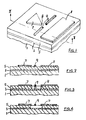
- the first device to be described comprises a sapphire base 1 on which is grown an undoped silicon layer 3.
- the free surface of the layer 3 carries a thermally-grown silicon dioxide layer 5 which is between 1 and 2»m thickness and is thereby able to withstand electric fields of 2 x 10⁸ volts/metre.
- the growth of this oxide layer preferably results in the complete oxidation of the layer 3.
- On this layer 5 there are formed three metallic electrode structures 7, 9, 11 constituting respectively the cathode, grid and anode of the device, as further explained below.
- the electrode structures are formed on the underlying silicon dioxide layer 5 by evaporation or sputtering of a metallic layer of a few tens of nanometres (a few hundred angstroms) to a few microns in thickness covering the layer 5.
- a lithographic technique is then used to etch through portions of the metallic layer selectively to produce the electrode shapes as shown in the figure.
- the cathode, grid and anode electrode structures 7, 9 and 11 respectively, thus formed are therefore coplanar.
- the whole device is then encapsulated, either as a single unit or with a number of similar devices formed on the same sapphire base, within a suitable evacuated enclosure (not shown).
- a voltage source (not shown) is connected across the cathode and anode electrode structures 7 and 11. Due to the high field gradients in the vicinity of the apex of the cathode electrode structure 7, that structure will have a lower electron emission threshold voltage than the anode electrode structure 11 and, for negative biases exceeding this threshold value, will emit electrons by an electron field emission process.
- the high electric field at the emission tip 8 of the cathode structure 7 is due to the thinness of the metal layer, the lithographic shaping in the plane of the layer, and its close proximity to the positively-biased grid 9 and/or anode 11 electrodes.
- the device may be made to operate as a rectifier, with a preferred direction of electron flow when the cathode is negative with respect to the anode structure.
- Suitable electrical biases may be applied to the grid electrode structure 9 in order to further modulate this electron flow.
- Non-linear characteristics suitable for digital switching applications may readily be achieved, and the operation of the device is particularly fast as its speed will not be limited by the velocity of sound, which normally limits the speed of operation of solid state devices.
- the difference in electron emissivity between the cathode and anode electrode structures may be enhanced further by choosing materials of different thicknesses, layers of different shapes in the electrode plane or materials of different work functions for these two structures. Any inhomogeneity in the material composition of the cathode structure will further enhance the local field strength, thereby also increasing the electron emissivity of the cathode electrode structure.
- the electron emissivity of the cathode electrode structure may also be increased by the implantation of suitable dopant materials, resulting in increased electron emission from the implanted sites.
- One particularly suitable dopant material is carbon. It will be appreciated that in some devices in accordance with the invention a layer of material such as carbon may advantageously be carried on the surface of the cathode structure rather than implanted therein.
- Figure 5 illustrates how a wide emission edge 12 of a cathode can be realized.
- Figure 5 shows a device in which a wide emission edge 12 of a cathode 13 allows a larger current flow than the cathode tip 8 of Figure 1.
- the gap between the cathode 13 and the anode 11 should be approximately 1»m, but will be dependent upon both the work function of the cathode 13 and the thickness of the metal of the cathode.
- a cathode electrode structure would be formed of a lower work function material than that of the anode structure.
- Figure 6 shows a device configuration in which a cathode electrode structure 17 is of needle-like form, the grid electrode structure comprising two similar needle-like conductive patterns 19 and 21 and the anode electrode structure 11 being of rectangular form as before.
- a cathode electrode structure 17 is of needle-like form
- the grid electrode structure comprising two similar needle-like conductive patterns 19 and 21 and the anode electrode structure 11 being of rectangular form as before.
- a cathode electrode structure 25 is of "V" formation.
- a grid electrode structure 27 is disposed round the tip of the "V" structure, so that particularly strong field gradients are present round the tip of the cathode 25.
- Such a disposition of the grid 27 should allow operation of the device with the grid biased negatively with respect to the cathode.
- the anode 11 would have to be approximately 1»m from the tip of the cathode 25 in order to allow operation with a 100 volt potential difference between the anode 11 and the cathode 25.
- this electrode structure will generally be formed from a material of higher work function than that of the cathode structure In order to avoid electron emission from the grid electrode structure.
- Such devices will, of course, require a two stage metallisation process in order to deposit the required electrode structures.
- such a two stage metallisation will also be required to provide a thicker anode structure, which will again give assymmetric current/voltage characteristics as a result of lower geometric field enhancement at the anode.
- Figure 8 shows a device in which an etched channel 23 is formed in a silicon dioxide layer 26, an initial metallisation of a low work function material 28 being followed by a metallisation of a high work function material 29 using the same masking structures.
- the upper metallised area within the channel 23 may be used as a grid electrode structure. Since the initial low work function layer 28 in the channel 23 is completely covered by the high work function layer 29, this grid electrode can be operated either positively or negatively with respect to the upper electrodes 30 and 31. It should be noted that the configuration of Figure 8 allows an operable device to be achieved with a close spacing of the cathode, anode and grid structures, irrespective of the number of metallisations.
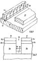
- Figure 9 shows a device in which a cathode electrode structure 32 is in the form of multiple undercut tips, and an anode electrode structure 33 is in the form of a rectangular strip, as before.
- a grid electrode structure 35 comprises a series of metallic pins 41 anchored to a doped stripe 37 in the underlying silicon 39.
- the electrode structures are carried on a layer of silicon dioxide grown from a layer of silicon, which is in turn carried on a sapphire base
- the electrode structures may be carried by any large band gap insulating substrate.
- the use of a sapphire base is particularly useful, however, as sapphire is a radiation hard material and is readily available with an epitaxial silicon layer, which can be oxidised to give an easily etchable substrate.
Landscapes
- Cold Cathode And The Manufacture (AREA)
Claims (16)
- Dispositif sous vide, pour émission par effet de champ, comportant un substrat (1), des moyens (7) formant électrode d'émission d'électrons pour émettre par effet de champ, des moyens (9) formant électrode de commande et des moyens (11) formant électrode de collecte d'électrons, tous ces moyens étant appliqués sur le substrat en une configuration substantiellement coplanaire et étant placés à l'intérieur d'un espace mis sous vide, dispositif dans lequel les électrons émis, par émission par effet de champ, par les moyens formant électrode d'émission s'écoulent vers les moyens formant électrode de collecte le long d'un chemin qui est substantiellement parallèle au substrat ; les moyens formant électrode de commande, pour réguler l'écoulement entre les moyens (7) formant électrode d'émission d'électrons et les moyens (11) formant électrode de collecte des électrons, se situant substantiellement à l'extérieur dudit chemin.
- Dispositif selon la revendication 1, caractérisé par le fait que les moyens (7) formant électrode d'émission présentent un travail de sortie moindre que les moyens (11) formant électrode de collecte, de sorte que les électrons sont préférentiellement émis par les moyens formant électrode d'émission.
- Dispositif selon la revendication 1, caractérisé par le fait que les moyens (7) formant électrode d'émission présentent un bord fin (12) en face des moyens (11) formant électrode de collecte, pour améliorer l'émission d'électrons de la part de la première structure d'électrode.
- Dispositif selon l'une quelconque des revendications précédentes, caractérisé par le fait que les moyens (7) formant électrode d'émission vont en s'effilant en direction des moyens (11) formant électrode de collecte, pour améliorer l'émission d'électrons de la part des moyens formant électrode d'émission.
- Dispositif selon la revendication 1 ou la revendication 2, caractérisé par le fait que les moyens (7) formant électrode d'émission contiennent un dope implanté pour améliorer l'émission d'électrons de la part des moyens formant électrode d'émission.
- Dispositif selon l'une quelconque des revendications précédentes, caractérisé par le fait que les moyens (7) formant électrode d'émission présentent un revêtement de surface pour améliorer l'émission d'électrons de la part des moyens formant électrode d'émission.
- Dispositif selon la revendication 1, caractérisé par un canal (23) dans le substrat (26) ; par une première portion d'une première couche conductrice (28) dans le canal ; et par une seconde et une troisième portion de la première couche conductrice sur le substrat, des côtés opposés, du canal, ladite première, ladite seconde et ladite troisième portion étant électriquement isolées l'une de l'autre et formant, respectivement, les moyens formant électrode de commande, les moyens formant électrode d'émission et les moyens formant électrode de collecte.
- Dispositif selon la revendication 7, caractérisé par une première, une seconde et une troisième portion d'une seconde couche conductrice (29) déposées sur ladite première, ladite seconde et ladite troisième portion, respectivement, de ladite première couche (28), le matériau de ladite seconde couche conductrice (29) présentant un travail de sortie supérieur à celui du matériau de ladite première couche conductrice (28).
- Procédé pour former un dispositif sous vide pour émission par effet de champ, consistant à appliquer sur un substrat commun (1), sous forme d'une construction substantiellement coplanaire, des moyens (7) formant électrode d'émission d'électrons pour émission par effet de champ, des moyens (9) formant électrode de commande et des moyens (11) formant électrode de collecte des électrons, pour que le flux d'électrons émis par émission par effet de champ s'écoule entre les moyens formant électrode d'émission et les moyens formant électrode de collecte le long d'un chemin substantiellement parallèle au substrat, en formant les moyens, formant électrode de commande et prévus pour réguler l'écoulement entre les moyens (7) formant électrode d'émission d'électrons et les moyens (11) formant électrode de collecte d'électrons, de façon qu'ils se trouvent substantiellement en dehors dudit chemin.
- Procédé selon la revendication 9, caractérisé par le fait que l'on forme une couche isolante (5) sur le substrat (1) ; que l'on forme une couche conductrice par dessus la couche isolante ; et que l'on élimine, par attaque chimique, une ou plusieurs portions de la couche conductrice pour laisser les zones de la couche conductrice formant les moyens (7, 9, 11) d'émission, de contrôle et de collecte, espacées l'une de l'autre.
- Procédé selon la revendication 10, caractérisé par le fait que l'on dépose une couche de silicium non dopée (3) sur le substrat (1) et, qu'à partir de cette couche, on fait croître thermiquement une couche de dioxyde de silicium pour former la couche isolante (5).
- Procédé selon la revendication 10 ou la revendication 11, caractérisé par le fait que l'on forme la couche conductrice par évaporation sous vide ou par pulvérisation cathodique d'un métal réfractaire , tel que le tungstène, le molybdène ou un matériau ou une combinaison de matériaux donnant une surface à faible travail de sortie.
- Procédé selon la revendication 10 ou la revendication 11, caractérisé par le fait que l'on implante un dope dans les moyens (7) formant électrode d'émission.
- Procédé comme revendiqué dans la revendication 10, caractérisé par le fait que l'on élimine par attaque chimique les portions de la couche isolante (5) situées entre les moyens (7, 9) formant électrode d'émission et de commande et entre les moyens (9, 11) formant électrode de commande et de collecte.
- Procédé selon la revendication 14, caractérisé par le fait qu'à la suite de l'élimination, par attaque chimique, des portions de la couche isolante (5), on affouille, par attaque chimique isotrope, la couche isolante située sous les bords, se faisant face, des structures formant électrode.
- Procédé selon la revendication 9, caractérisé par le fait que l'on forme une couche isolante (26) sur le substrat ; que, par attaque chimique, on forme un canal (23) dans la couche isolante ; que, par dessus la couche isolante, on dépose une première couche (28) d'un matériau présentant un faible travail de sortie ; et que, par dessus la première couche, on dépose une seconde couche (29) d'un matériau présentant un fort travail de sortie ; étant précisé que la profondeur du canal est suffisante pour que la portion de la première et de la seconde couche se trouvant à l'intérieur du canal soit séparée des portions qui se trouvent de chaque côté du canal, de sorte que les moyens (30, 31) formant électrode d'émission et de collecte sont formés de chaque côté du canal et les moyens formant électrode de commande sont formés à l'intérieur du canal.
Applications Claiming Priority (2)
| Application Number | Priority Date | Filing Date | Title |
|---|---|---|---|
| GB8621600 | 1986-09-08 | ||
| GB868621600A GB8621600D0 (en) | 1986-09-08 | 1986-09-08 | Vacuum devices |
Publications (3)
| Publication Number | Publication Date |
|---|---|
| EP0260075A2 EP0260075A2 (fr) | 1988-03-16 |
| EP0260075A3 EP0260075A3 (en) | 1989-05-10 |
| EP0260075B1 true EP0260075B1 (fr) | 1994-06-08 |
Family
ID=10603843
Family Applications (1)
| Application Number | Title | Priority Date | Filing Date |
|---|---|---|---|
| EP87307818A Expired - Lifetime EP0260075B1 (fr) | 1986-09-08 | 1987-09-04 | Dispositifs de vide |
Country Status (4)
| Country | Link |
|---|---|
| US (1) | US4827177A (fr) |
| EP (1) | EP0260075B1 (fr) |
| DE (1) | DE3750007T2 (fr) |
| GB (2) | GB8621600D0 (fr) |
Families Citing this family (108)
| Publication number | Priority date | Publication date | Assignee | Title |
|---|---|---|---|---|
| US4904895A (en) * | 1987-05-06 | 1990-02-27 | Canon Kabushiki Kaisha | Electron emission device |
| GB8720792D0 (en) * | 1987-09-04 | 1987-10-14 | Gen Electric Co Plc | Vacuum devices |
| CA1330827C (fr) * | 1988-01-06 | 1994-07-19 | Jupiter Toy Company | Production et manipulation de charges haute densite |
| US5153901A (en) * | 1988-01-06 | 1992-10-06 | Jupiter Toy Company | Production and manipulation of charged particles |
| US5123039A (en) * | 1988-01-06 | 1992-06-16 | Jupiter Toy Company | Energy conversion using high charge density |
| US5054046A (en) * | 1988-01-06 | 1991-10-01 | Jupiter Toy Company | Method of and apparatus for production and manipulation of high density charge |
| DE3817897A1 (de) * | 1988-01-06 | 1989-07-20 | Jupiter Toy Co | Die erzeugung und handhabung von ladungsgebilden hoher ladungsdichte |
| GB2218257B (en) * | 1988-05-03 | 1992-12-23 | Jupiter Toy Co | Apparatus for producing and manipulating charged particles. |
| US5018180A (en) * | 1988-05-03 | 1991-05-21 | Jupiter Toy Company | Energy conversion using high charge density |
| JP2630988B2 (ja) * | 1988-05-26 | 1997-07-16 | キヤノン株式会社 | 電子線発生装置 |
| US5285129A (en) * | 1988-05-31 | 1994-02-08 | Canon Kabushiki Kaisha | Segmented electron emission device |
| DE68926090D1 (de) * | 1988-10-17 | 1996-05-02 | Matsushita Electric Industrial Co Ltd | Feldemissions-Kathoden |
| JP2981751B2 (ja) * | 1989-03-23 | 1999-11-22 | キヤノン株式会社 | 電子線発生装置及びこれを用いた画像形成装置、並びに電子線発生装置の製造方法 |
| US4990766A (en) * | 1989-05-22 | 1991-02-05 | Murasa International | Solid state electron amplifier |
| WO1992015111A1 (fr) * | 1989-06-12 | 1992-09-03 | Hickstech Corp. | Amplificateur d'electrons et son procede de fabrication |
| US5003216A (en) * | 1989-06-12 | 1991-03-26 | Hickstech Corp. | Electron amplifier and method of manufacture therefor |
| US5217401A (en) * | 1989-07-07 | 1993-06-08 | Matsushita Electric Industrial Co., Ltd. | Method of manufacturing a field-emission type switching device |
| JPH0340332A (ja) * | 1989-07-07 | 1991-02-21 | Matsushita Electric Ind Co Ltd | 電界放出型スウィチング素子およびその製造方法 |
| US4956574A (en) * | 1989-08-08 | 1990-09-11 | Motorola, Inc. | Switched anode field emission device |
| EP0500543A4 (en) * | 1989-09-29 | 1992-11-19 | Motorola, Inc. | Flat panel display using field emission devices |
| US5019003A (en) * | 1989-09-29 | 1991-05-28 | Motorola, Inc. | Field emission device having preformed emitters |
| US5055077A (en) * | 1989-11-22 | 1991-10-08 | Motorola, Inc. | Cold cathode field emission device having an electrode in an encapsulating layer |
| EP0434001B1 (fr) * | 1989-12-19 | 1996-04-03 | Matsushita Electric Industrial Co., Ltd. | Dispositif à émission de champ et son procédé de fabrication |
| US5267884A (en) * | 1990-01-29 | 1993-12-07 | Mitsubishi Denki Kabushiki Kaisha | Microminiature vacuum tube and production method |
| JP2968014B2 (ja) * | 1990-01-29 | 1999-10-25 | 三菱電機株式会社 | 微小真空管及びその製造方法 |
| US5079476A (en) * | 1990-02-09 | 1992-01-07 | Motorola, Inc. | Encapsulated field emission device |
| US5142184B1 (en) * | 1990-02-09 | 1995-11-21 | Motorola Inc | Cold cathode field emission device with integral emitter ballasting |
| US5030921A (en) * | 1990-02-09 | 1991-07-09 | Motorola, Inc. | Cascaded cold cathode field emission devices |
| US5007873A (en) * | 1990-02-09 | 1991-04-16 | Motorola, Inc. | Non-planar field emission device having an emitter formed with a substantially normal vapor deposition process |
| US5192240A (en) * | 1990-02-22 | 1993-03-09 | Seiko Epson Corporation | Method of manufacturing a microelectronic vacuum device |
| US5214346A (en) * | 1990-02-22 | 1993-05-25 | Seiko Epson Corporation | Microelectronic vacuum field emission device |
| JP2574500B2 (ja) * | 1990-03-01 | 1997-01-22 | 松下電器産業株式会社 | プレーナ型冷陰極の製造方法 |
| US5214347A (en) * | 1990-06-08 | 1993-05-25 | The United States Of America As Represented By The Secretary Of The Navy | Layered thin-edged field-emitter device |
| US5266155A (en) * | 1990-06-08 | 1993-11-30 | The United States Of America As Represented By The Secretary Of The Navy | Method for making a symmetrical layered thin film edge field-emitter-array |
| US5461280A (en) * | 1990-08-29 | 1995-10-24 | Motorola | Field emission device employing photon-enhanced electron emission |
| US5148078A (en) * | 1990-08-29 | 1992-09-15 | Motorola, Inc. | Field emission device employing a concentric post |
| US5030895A (en) * | 1990-08-30 | 1991-07-09 | The United States Of America As Represented By The Secretary Of The Navy | Field emitter array comparator |
| EP0504370A4 (en) * | 1990-09-07 | 1992-12-23 | Motorola, Inc. | A field emission device employing a layer of single-crystal silicon |
| US5157309A (en) * | 1990-09-13 | 1992-10-20 | Motorola Inc. | Cold-cathode field emission device employing a current source means |
| US5136764A (en) * | 1990-09-27 | 1992-08-11 | Motorola, Inc. | Method for forming a field emission device |
| JP2613669B2 (ja) * | 1990-09-27 | 1997-05-28 | 工業技術院長 | 電界放出素子及びその製造方法 |
| US5281890A (en) * | 1990-10-30 | 1994-01-25 | Motorola, Inc. | Field emission device having a central anode |
| US5469015A (en) * | 1990-11-28 | 1995-11-21 | Matsushita Electric Industrial Co., Ltd. | Functional vacuum microelectronic field-emission device |
| DE69128702T2 (de) * | 1990-11-28 | 1998-04-23 | Matsushita Electric Ind Co Ltd | Mikroelektronische Feldemissionsvorrichtung |
| US5173634A (en) * | 1990-11-30 | 1992-12-22 | Motorola, Inc. | Current regulated field-emission device |
| US5173635A (en) * | 1990-11-30 | 1992-12-22 | Motorola, Inc. | Bi-directional field emission device |
| US5204588A (en) * | 1991-01-14 | 1993-04-20 | Sony Corporation | Quantum phase interference transistor |
| US5112436A (en) * | 1990-12-24 | 1992-05-12 | Xerox Corporation | Method of forming planar vacuum microelectronic devices with self aligned anode |
| US5432407A (en) * | 1990-12-26 | 1995-07-11 | Motorola, Inc. | Field emission device as charge transport switch for energy storage network |
| JP2613697B2 (ja) | 1991-01-16 | 1997-05-28 | 工業技術院長 | 電界放出素子 |
| US5212426A (en) * | 1991-01-24 | 1993-05-18 | Motorola, Inc. | Integrally controlled field emission flat display device |
| US5075595A (en) * | 1991-01-24 | 1991-12-24 | Motorola, Inc. | Field emission device with vertically integrated active control |
| US5218273A (en) * | 1991-01-25 | 1993-06-08 | Motorola, Inc. | Multi-function field emission device |
| US5281891A (en) * | 1991-02-22 | 1994-01-25 | Matsushita Electric Industrial Co., Ltd. | Electron emission element |
| US5140219A (en) * | 1991-02-28 | 1992-08-18 | Motorola, Inc. | Field emission display device employing an integral planar field emission control device |
| US5142256A (en) * | 1991-04-04 | 1992-08-25 | Motorola, Inc. | Pin diode with field emission device switch |
| JP3235172B2 (ja) * | 1991-05-13 | 2001-12-04 | セイコーエプソン株式会社 | 電界電子放出装置 |
| US5343110A (en) * | 1991-06-04 | 1994-08-30 | Matsushita Electric Industrial Co., Ltd. | Electron emission element |
| US5144191A (en) * | 1991-06-12 | 1992-09-01 | Mcnc | Horizontal microelectronic field emission devices |
| US5233263A (en) * | 1991-06-27 | 1993-08-03 | International Business Machines Corporation | Lateral field emission devices |
| US5384509A (en) * | 1991-07-18 | 1995-01-24 | Motorola, Inc. | Field emission device with horizontal emitter |
| US5227699A (en) * | 1991-08-16 | 1993-07-13 | Amoco Corporation | Recessed gate field emission |
| JP3072795B2 (ja) * | 1991-10-08 | 2000-08-07 | キヤノン株式会社 | 電子放出素子と該素子を用いた電子線発生装置及び画像形成装置 |
| US5536193A (en) * | 1991-11-07 | 1996-07-16 | Microelectronics And Computer Technology Corporation | Method of making wide band gap field emitter |
| US5763997A (en) * | 1992-03-16 | 1998-06-09 | Si Diamond Technology, Inc. | Field emission display device |
| US5449970A (en) * | 1992-03-16 | 1995-09-12 | Microelectronics And Computer Technology Corporation | Diode structure flat panel display |
| US6127773A (en) * | 1992-03-16 | 2000-10-03 | Si Diamond Technology, Inc. | Amorphic diamond film flat field emission cathode |
| US5686791A (en) * | 1992-03-16 | 1997-11-11 | Microelectronics And Computer Technology Corp. | Amorphic diamond film flat field emission cathode |
| US5543684A (en) | 1992-03-16 | 1996-08-06 | Microelectronics And Computer Technology Corporation | Flat panel display based on diamond thin films |
| US5675216A (en) * | 1992-03-16 | 1997-10-07 | Microelectronics And Computer Technololgy Corp. | Amorphic diamond film flat field emission cathode |
| US5409568A (en) * | 1992-08-04 | 1995-04-25 | Vasche; Gregory S. | Method of fabricating a microelectronic vacuum triode structure |
| US5312777A (en) * | 1992-09-25 | 1994-05-17 | International Business Machines Corporation | Fabrication methods for bidirectional field emission devices and storage structures |
| JPH08138561A (ja) * | 1992-12-07 | 1996-05-31 | Mitsuteru Kimura | 微小真空デバイス |
| KR100307384B1 (ko) * | 1993-01-19 | 2001-12-17 | 레오니드 다니로비치 카르포브 | 전계방출장치 |
| JP3726117B2 (ja) * | 1993-11-04 | 2005-12-14 | ナノ・プラプライアテリ、インク | 平坦パネル・ディスプレイ・システムと構成部品とを製造する方法 |
| US5445550A (en) * | 1993-12-22 | 1995-08-29 | Xie; Chenggang | Lateral field emitter device and method of manufacturing same |
| US5629580A (en) * | 1994-10-28 | 1997-05-13 | International Business Machines Corporation | Lateral field emission devices for display elements and methods of fabrication |
| KR100322696B1 (ko) * | 1995-03-29 | 2002-06-20 | 김순택 | 전계효과전자방출용마이크로-팁및그제조방법 |
| US5713775A (en) * | 1995-05-02 | 1998-02-03 | Massachusetts Institute Of Technology | Field emitters of wide-bandgap materials and methods for their fabrication |
| US5630741A (en) * | 1995-05-08 | 1997-05-20 | Advanced Vision Technologies, Inc. | Fabrication process for a field emission display cell structure |
| US5644188A (en) * | 1995-05-08 | 1997-07-01 | Advanced Vision Technologies, Inc. | Field emission display cell structure |
| JPH11510639A (ja) * | 1995-06-02 | 1999-09-14 | アドバンスド ビジョン テクノロジーズ,インコーポレイテッド | 簡略陽極を具備した側方エミッタ電界放出デバイスおよびその製造法 |
| US5811929A (en) * | 1995-06-02 | 1998-09-22 | Advanced Vision Technologies, Inc. | Lateral-emitter field-emission device with simplified anode |
| US5647998A (en) * | 1995-06-13 | 1997-07-15 | Advanced Vision Technologies, Inc. | Fabrication process for laminar composite lateral field-emission cathode |
| US5703380A (en) * | 1995-06-13 | 1997-12-30 | Advanced Vision Technologies Inc. | Laminar composite lateral field-emission cathode |
| US5644190A (en) * | 1995-07-05 | 1997-07-01 | Advanced Vision Technologies, Inc. | Direct electron injection field-emission display device |
| US5616061A (en) * | 1995-07-05 | 1997-04-01 | Advanced Vision Technologies, Inc. | Fabrication process for direct electron injection field-emission display device |
| US5666019A (en) * | 1995-09-06 | 1997-09-09 | Advanced Vision Technologies, Inc. | High-frequency field-emission device |
| US5628663A (en) * | 1995-09-06 | 1997-05-13 | Advanced Vision Technologies, Inc. | Fabrication process for high-frequency field-emission device |
| US5872421A (en) * | 1996-12-30 | 1999-02-16 | Advanced Vision Technologies, Inc. | Surface electron display device with electron sink |
| US6015324A (en) * | 1996-12-30 | 2000-01-18 | Advanced Vision Technologies, Inc. | Fabrication process for surface electron display device with electron sink |
| US5828163A (en) * | 1997-01-13 | 1998-10-27 | Fed Corporation | Field emitter device with a current limiter structure |
| EP1716926A3 (fr) * | 2000-04-13 | 2007-08-29 | Wako Pure Chemical Industries Ltd | Construction d'électrode pour appareil diélectrophorétique et séparation par diélectrophorèse |
| US7259510B1 (en) * | 2000-08-30 | 2007-08-21 | Agere Systems Inc. | On-chip vacuum tube device and process for making device |
| JP3703415B2 (ja) * | 2001-09-07 | 2005-10-05 | キヤノン株式会社 | 電子放出素子、電子源及び画像形成装置、並びに電子放出素子及び電子源の製造方法 |
| KR20050076454A (ko) * | 2004-01-20 | 2005-07-26 | 삼성에스디아이 주식회사 | 전계방출형 백라이트 장치 |
| KR20070010660A (ko) * | 2005-07-19 | 2007-01-24 | 삼성에스디아이 주식회사 | 전자 방출 소자 및 이를 구비한 평판 디스플레이 장치 |
| KR20070011804A (ko) * | 2005-07-21 | 2007-01-25 | 삼성에스디아이 주식회사 | 전자 방출 소자 및 이를 구비한 평판 디스플레이 장치 |
| TWI260669B (en) * | 2005-07-26 | 2006-08-21 | Ind Tech Res Inst | Field emission light-emitting device |
| KR100706799B1 (ko) * | 2005-10-07 | 2007-04-12 | 삼성전자주식회사 | 필라멘트 부재 및 이를 가지는 이온 주입 장치의 이온 소스 |
| CN100583350C (zh) * | 2006-07-19 | 2010-01-20 | 清华大学 | 微型场发射电子器件 |
| US8159119B2 (en) * | 2007-11-30 | 2012-04-17 | Electronics And Telecommunications Research Institute | Vacuum channel transistor and manufacturing method thereof |
| KR101042962B1 (ko) * | 2008-10-29 | 2011-06-20 | 한국전자통신연구원 | 열음극 전자방출 진공 채널 트랜지스터, 다이오드 및 그 진공 채널 트랜지스터의 제조방법 |
| US9680116B2 (en) | 2015-09-02 | 2017-06-13 | International Business Machines Corporation | Carbon nanotube vacuum transistors |
| US9805900B1 (en) * | 2016-05-04 | 2017-10-31 | Lockheed Martin Corporation | Two-dimensional graphene cold cathode, anode, and grid |
| CN110875165A (zh) * | 2018-08-30 | 2020-03-10 | 中国科学院微电子研究所 | 一种场发射阴极电子源及其阵列 |
| US10937620B2 (en) * | 2018-09-26 | 2021-03-02 | International Business Machines Corporation | Vacuum channel transistor structures with sub-10 nanometer nanogaps and layered metal electrodes |
| CN119297060A (zh) * | 2024-09-24 | 2025-01-10 | 中山大学 | 基于梯形栅极结构的氮化镓平面微纳真空三极管 |
Citations (3)
| Publication number | Priority date | Publication date | Assignee | Title |
|---|---|---|---|---|
| US3678325A (en) * | 1969-03-14 | 1972-07-18 | Matsushita Electric Industrial Co Ltd | High-field emission cathodes and methods for preparing the cathodes |
| US3748522A (en) * | 1969-10-06 | 1973-07-24 | Stanford Research Inst | Integrated vacuum circuits |
| GB2054959A (en) * | 1979-07-13 | 1981-02-18 | Philips Nv | Reverse biased p-n junction cathode |
Family Cites Families (10)
| Publication number | Priority date | Publication date | Assignee | Title |
|---|---|---|---|---|
| FR1204367A (fr) * | 1958-03-24 | 1960-01-26 | Csf | Cathode thermoélectronique froide à semi-conducteur |
| GB888955A (en) * | 1958-05-14 | 1962-02-07 | Standard Telephones Cables Ltd | Improvements in electron discharge devices |
| US3359448A (en) * | 1964-11-04 | 1967-12-19 | Research Corp | Low work function thin film gap emitter |
| US3788723A (en) * | 1972-04-24 | 1974-01-29 | Fairchild Camera Instr Co | Method of preparing cavity envelopes by means of thin-film procedures |
| DE3133786A1 (de) * | 1981-08-26 | 1983-03-10 | Battelle-Institut E.V., 6000 Frankfurt | Anordnung zur erzeugung von feldemission und verfahren zu ihrer herstellung |
| NL8104893A (nl) * | 1981-10-29 | 1983-05-16 | Philips Nv | Kathodestraalbuis en halfgeleiderinrichting voor toepassing in een dergelijke kathodestraalbuis. |
| US4728851A (en) * | 1982-01-08 | 1988-03-01 | Ford Motor Company | Field emitter device with gated memory |
| US4578614A (en) * | 1982-07-23 | 1986-03-25 | The United States Of America As Represented By The Secretary Of The Navy | Ultra-fast field emitter array vacuum integrated circuit switching device |
| US4712039A (en) * | 1986-04-11 | 1987-12-08 | Hong Lazaro M | Vacuum integrated circuit |
| US4904895A (en) * | 1987-05-06 | 1990-02-27 | Canon Kabushiki Kaisha | Electron emission device |
-
1986
- 1986-09-08 GB GB868621600A patent/GB8621600D0/en active Pending
-
1987
- 1987-08-05 GB GB8718514A patent/GB2195046B/en not_active Expired - Lifetime
- 1987-09-03 US US07/092,426 patent/US4827177A/en not_active Expired - Fee Related
- 1987-09-04 EP EP87307818A patent/EP0260075B1/fr not_active Expired - Lifetime
- 1987-09-04 DE DE3750007T patent/DE3750007T2/de not_active Expired - Fee Related
Patent Citations (3)
| Publication number | Priority date | Publication date | Assignee | Title |
|---|---|---|---|---|
| US3678325A (en) * | 1969-03-14 | 1972-07-18 | Matsushita Electric Industrial Co Ltd | High-field emission cathodes and methods for preparing the cathodes |
| US3748522A (en) * | 1969-10-06 | 1973-07-24 | Stanford Research Inst | Integrated vacuum circuits |
| GB2054959A (en) * | 1979-07-13 | 1981-02-18 | Philips Nv | Reverse biased p-n junction cathode |
Non-Patent Citations (2)
| Title |
|---|
| Japanese Journal of Applied Physics, vol. 10, no. 6, June 1971, pp. 781-785 * |
| Journal of the Electrochemical Society, vol. 133, 1986, pp. 446-447 * |
Also Published As
| Publication number | Publication date |
|---|---|
| DE3750007T2 (de) | 1994-10-06 |
| DE3750007D1 (de) | 1994-07-14 |
| GB2195046A (en) | 1988-03-23 |
| GB2195046B (en) | 1990-07-11 |
| EP0260075A2 (fr) | 1988-03-16 |
| US4827177A (en) | 1989-05-02 |
| EP0260075A3 (en) | 1989-05-10 |
| GB8718514D0 (en) | 1987-10-21 |
| GB8621600D0 (en) | 1987-03-18 |
Similar Documents
| Publication | Publication Date | Title |
|---|---|---|
| EP0260075B1 (fr) | Dispositifs de vide | |
| US6333598B1 (en) | Low gate current field emitter cell and array with vertical thin-film-edge emitter | |
| US6629869B1 (en) | Method of making flat panel displays having diamond thin film cathode | |
| US5528099A (en) | Lateral field emitter device | |
| US6373175B1 (en) | Electronic switching devices | |
| US4956574A (en) | Switched anode field emission device | |
| US5757344A (en) | Cold cathode emitter element | |
| US6590322B2 (en) | Low gate current field emitter cell and array with vertical thin-film-edge emitter | |
| JPS6146931B2 (fr) | ||
| US7102157B2 (en) | Nanotube-based vacuum devices | |
| JPH0340332A (ja) | 電界放出型スウィチング素子およびその製造方法 | |
| EP1003195A3 (fr) | Source d'électrons à émission de champs, procédé pour sa fabrication et dispositif d'affichage avec une telle source d'électrons | |
| EP1047095A3 (fr) | Cathode à émission par effet de champ et procédé de fabrication | |
| Park et al. | Lateral field emission diodes using SIMOX wafer | |
| US7176478B2 (en) | Nanotube-based vacuum devices | |
| JP2763219B2 (ja) | 電界放出型電子素子 | |
| JPH0748346B2 (ja) | 電界放出冷陰極素子 | |
| US5680011A (en) | Cold cathode density-modulated type electron gun and microwave tube using the same | |
| JPH07118270B2 (ja) | カーボンナノチューブトランジスタ | |
| JP3266503B2 (ja) | 側面電界放出素子のための最適ゲート制御設計及び製作方法 | |
| Gray et al. | A silicon field emitter array planar vacuum FET fabricated with microfabrication techniques | |
| US6777169B2 (en) | Method of forming emitter tips for use in a field emission display | |
| US6351254B2 (en) | Junction-based field emission structure for field emission display | |
| JP3444943B2 (ja) | 冷陰極電子源素子 | |
| JP2601085B2 (ja) | 機能性電子放出素子およびその製造方法 |
Legal Events
| Date | Code | Title | Description |
|---|---|---|---|
| PUAI | Public reference made under article 153(3) epc to a published international application that has entered the european phase |
Free format text: ORIGINAL CODE: 0009012 |
|
| AK | Designated contracting states |
Kind code of ref document: A2 Designated state(s): DE FR IT NL |
|
| PUAL | Search report despatched |
Free format text: ORIGINAL CODE: 0009013 |
|
| AK | Designated contracting states |
Kind code of ref document: A3 Designated state(s): DE FR IT NL |
|
| 17P | Request for examination filed |
Effective date: 19891110 |
|
| 17Q | First examination report despatched |
Effective date: 19920218 |
|
| GRAA | (expected) grant |
Free format text: ORIGINAL CODE: 0009210 |
|
| AK | Designated contracting states |
Kind code of ref document: B1 Designated state(s): DE FR IT NL |
|
| ITF | It: translation for a ep patent filed | ||
| ET | Fr: translation filed | ||
| REF | Corresponds to: |
Ref document number: 3750007 Country of ref document: DE Date of ref document: 19940714 |
|
| PG25 | Lapsed in a contracting state [announced via postgrant information from national office to epo] |
Ref country code: NL Effective date: 19950401 |
|
| PLBE | No opposition filed within time limit |
Free format text: ORIGINAL CODE: 0009261 |
|
| STAA | Information on the status of an ep patent application or granted ep patent |
Free format text: STATUS: NO OPPOSITION FILED WITHIN TIME LIMIT |
|
| NLV4 | Nl: lapsed or anulled due to non-payment of the annual fee | ||
| 26N | No opposition filed | ||
| PG25 | Lapsed in a contracting state [announced via postgrant information from national office to epo] |
Ref country code: FR Effective date: 19950531 |
|
| PG25 | Lapsed in a contracting state [announced via postgrant information from national office to epo] |
Ref country code: DE Effective date: 19950601 |
|
| REG | Reference to a national code |
Ref country code: FR Ref legal event code: ST |
|
| PG25 | Lapsed in a contracting state [announced via postgrant information from national office to epo] |
Ref country code: IT Free format text: LAPSE BECAUSE OF NON-PAYMENT OF DUE FEES;WARNING: LAPSES OF ITALIAN PATENTS WITH EFFECTIVE DATE BEFORE 2007 MAY HAVE OCCURRED AT ANY TIME BEFORE 2007. THE CORRECT EFFECTIVE DATE MAY BE DIFFERENT FROM THE ONE RECORDED. Effective date: 20050904 |