EP0260110A2 - Diode électroluminescente à double hétérostructure - Google Patents
Diode électroluminescente à double hétérostructure Download PDFInfo
- Publication number
- EP0260110A2 EP0260110A2 EP19870307928 EP87307928A EP0260110A2 EP 0260110 A2 EP0260110 A2 EP 0260110A2 EP 19870307928 EP19870307928 EP 19870307928 EP 87307928 A EP87307928 A EP 87307928A EP 0260110 A2 EP0260110 A2 EP 0260110A2
- Authority
- EP
- European Patent Office
- Prior art keywords
- light emitting
- active layer
- emitting diode
- double heterostructure
- layer
- Prior art date
- Legal status (The legal status is an assumption and is not a legal conclusion. Google has not performed a legal analysis and makes no representation as to the accuracy of the status listed.)
- Granted
Links
Images
Classifications
-
- H—ELECTRICITY
- H10—SEMICONDUCTOR DEVICES; ELECTRIC SOLID-STATE DEVICES NOT OTHERWISE PROVIDED FOR
- H10H—INORGANIC LIGHT-EMITTING SEMICONDUCTOR DEVICES HAVING POTENTIAL BARRIERS
- H10H20/00—Individual inorganic light-emitting semiconductor devices having potential barriers, e.g. light-emitting diodes [LED]
- H10H20/80—Constructional details
- H10H20/81—Bodies
- H10H20/822—Materials of the light-emitting regions
- H10H20/824—Materials of the light-emitting regions comprising only Group III-V materials, e.g. GaP
- H10H20/8242—Materials of the light-emitting regions comprising only Group III-V materials, e.g. GaP characterised by the dopants
-
- H—ELECTRICITY
- H10—SEMICONDUCTOR DEVICES; ELECTRIC SOLID-STATE DEVICES NOT OTHERWISE PROVIDED FOR
- H10H—INORGANIC LIGHT-EMITTING SEMICONDUCTOR DEVICES HAVING POTENTIAL BARRIERS
- H10H20/00—Individual inorganic light-emitting semiconductor devices having potential barriers, e.g. light-emitting diodes [LED]
- H10H20/80—Constructional details
- H10H20/81—Bodies
- H10H20/811—Bodies having quantum effect structures or superlattices, e.g. tunnel junctions
-
- H—ELECTRICITY
- H10—SEMICONDUCTOR DEVICES; ELECTRIC SOLID-STATE DEVICES NOT OTHERWISE PROVIDED FOR
- H10H—INORGANIC LIGHT-EMITTING SEMICONDUCTOR DEVICES HAVING POTENTIAL BARRIERS
- H10H20/00—Individual inorganic light-emitting semiconductor devices having potential barriers, e.g. light-emitting diodes [LED]
- H10H20/80—Constructional details
- H10H20/81—Bodies
- H10H20/822—Materials of the light-emitting regions
- H10H20/824—Materials of the light-emitting regions comprising only Group III-V materials, e.g. GaP
Definitions
- the invention relates to a double heterostructure light emitting diode, and more particularly to a double heterostructure light emitting diode which is used for a light source in an optical communication system and so on.
- the double heterostructure light emitting diode comprises a buffer layer of Sn doped n-InP, an active layer of Zn doped p+ -InGaAsP, a cladding layer of Zn doped p-InP, a confining layer of Sn doped n-InGaAsP, a capping layer of Zn doped p-InGaAsP, and a SiO2 film respectively in turn provided on an n-InP substrate.
- the double heterostructure light emitting diode further comprises a p-electrode provided on the SiO2 film, an n-electrode having a light emitting window provided on the back surface of the n-InP substrate, and a Zn diffused region of a predetermined diameter built in the confining layer wherein the p-electrode is partly projected into a current injecting aperture of the SiO2 film to be in contact with the Zn-diffused region extending through the capping layer over the confining layer.
- the active layer is heavily doped with p-impurity like Zn to shorten the life time of carriers so that a high speed response is obtained.
- a rise and fall times of light input are both as fast as 350 ps using a specified speedup circuit and applying DC bias offset.
- a peaking of pulses is performed in a rise and fall thereof in a circuit for driving a light emitting diode, or that DC biased voltage is applied thereto to obtain a high speed response, if an active layer thereof is not heavily doped with a p-impurity.
- a double heterostructure light emitting diode comprises, a double heterostructure provided on a semiconductor substrate including a p-active layer, and n and p-cladding layers respectively provided on the both sides of said p-active layer, and means for applying a predetermined level of voltage across said n and p-cladding layers, wherein said p-active layer is doped with a p-impurity such that the impurity concentration is distributed therein to be higher in a region proximate to the p-n junction between said p-active and n-cladding layers.
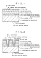
- a double heterostructure light emitting diode in the first embodiment according to the invention.
- an n-cladding layer 12 of n-InP In fabricating the double heterostructure light emitting diode, an n-cladding layer 12 of n-InP, a p-high concentration region 13 of p-InGaAsP which is doped with Zn by 1x1019 cm ⁇ 3 in its concentration to be of 0.1 ⁇ m in its thickness, a p-low concentration region 14 of p-In-GaAsP which is doped with Zn by 7x1018cm ⁇ 3 in its concentration to be of 14 ⁇ m in its thickness, a p-cladding layer 15 of InP, and a contact layer 16 of p-InGaAsP are sequentially provided on a semiconductor substrate 11 of n-InP.
- an active layer 30 is composed of the p-high and low concentration regions 13 and 14.
- a SiO2 film 17 is provided on the contact layer 16, and a current injecting aperture 18 is then formed to be of 20 ⁇ m in its diameter in accordance with the preferential etching of the SiO2 film covered with a photoresist. Thereafter, a p-electrode 19 of TiPt film is provided on the SiO2 film 17 and in the current injecting aperture 18.
- an n-electrode 21 of AuGe film is provided so as to have a light emitting window 20 on the back surface of the semiconductor substrate 11 which is polished to be of approximately 100 ⁇ m in its thickness.
- the p-high concentration region 13 is provided in the active layer 30 to be in contact with a p-n junction so that a higher speed of electron-hole recombination is obtained in the p-high concentration region 13.
- a fall time of light output is shortened by more than 40% in the first embodiment according to the invention, as far as light output is maintained to be the same level.
- light output is increased in its level as much as approximately 50% in a case where a fall time thereof is maitained to be the same as that in the conventional light emitting diode.
- a yield in fabricating a double heterostructure light emitting diode according to the invention is improved for the reason why a roughness on the surface of the p-high concentration region 13 is no matter in regard to a characteristic thereof because the p-low concentration region 14 is provided directly thereon to provide the active layer 30.
- a double heterostructure light emitting diode in the second embodiment wherein like parts are designated by like reference numerals except that a SiO2 film, current injecting aperture and p-electrode are designated respectively by 17a, 18a and 19a so that repeated explanations are omitted here.
- the double heterostructure light emitting diode is provided with a circular groove 22 being extended through an active layer 30 thereby resulting in a current confining therein, although a p-impurity concentration is distributed in the active layer 30 in the same manner as the first embodiment.
- a parasitic capacitance is much decreased in the existence of the groove 22 so that a response time is much more shortened. Further, an efficiency in coupling light from the light emitting diode to an optical fiber is improved to a great extent for the reason why light emitting intensity is distributed uniformly because current is transversely confined by the groove 22.
- a fall time of light output is shortened as much as a half, while light output is increased in its level as much as 60% in the second embodiment.
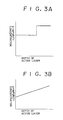
- a p-impurity concentration is distributed in the active layer 30 to be varied in a step-like manner in a direction of thickness thereof as shown in Fig. 3A, it may be varied gradually in a continuous manner as shown in Fig. 3B thereby to result in the same effects.
- Such a distribution of p-impurity concentration is easily carried out by a vapour phase epitaxial growth method.
- carriers injected into the active layer 30 are extinguished in accordance with the recombination thereof during the time when a voltage applied across the p and n-electrodes 19 and 21 becomes zero due to the turning off of a driving pulse applied thereacross.
- a fall time of light output is determined by the extinction of electrons in the active layer 30 because the active layer 30 is doped with p-impurity. At this moment, electrons are collected along the p-n junction in the active layer 30, that is, on the side of the n-cladding layer 12 due to the space charge of the p-n junction.
- a p-impurity concentration is distributed to be higher in the region proximate to the p-n junction in the active layer 30, in other words, a p-impurity concentration is higher in the region where electrons are collected.
- a fall time of light output is extremely shortened.
Landscapes
- Led Devices (AREA)
Applications Claiming Priority (2)
| Application Number | Priority Date | Filing Date | Title |
|---|---|---|---|
| JP216505/86 | 1986-09-12 | ||
| JP21650586A JPH071798B2 (ja) | 1986-09-12 | 1986-09-12 | 発光ダイオ−ド |
Publications (3)
| Publication Number | Publication Date |
|---|---|
| EP0260110A2 true EP0260110A2 (fr) | 1988-03-16 |
| EP0260110A3 EP0260110A3 (en) | 1989-04-05 |
| EP0260110B1 EP0260110B1 (fr) | 1992-07-08 |
Family
ID=16689479
Family Applications (1)
| Application Number | Title | Priority Date | Filing Date |
|---|---|---|---|
| EP87307928A Expired EP0260110B1 (fr) | 1986-09-12 | 1987-09-08 | Diode électroluminescente à double hétérostructure |
Country Status (4)
| Country | Link |
|---|---|
| US (1) | US4862230A (fr) |
| EP (1) | EP0260110B1 (fr) |
| JP (1) | JPH071798B2 (fr) |
| DE (1) | DE3780239T2 (fr) |
Cited By (2)
| Publication number | Priority date | Publication date | Assignee | Title |
|---|---|---|---|---|
| US5763906A (en) * | 1994-08-01 | 1998-06-09 | The Secretary Of State For Defence In Her Britannic Majesty's Government Of The United Kingdom Of Great Britian And Northern Ireland | Mid infrared light emitting diode |
| WO2000019545A1 (fr) * | 1998-09-30 | 2000-04-06 | Osram Opto Semiconductors Gmbh & Co. Ohg | Source de rayonnement de diode a emission par la surface |
Families Citing this family (7)
| Publication number | Priority date | Publication date | Assignee | Title |
|---|---|---|---|---|
| JPH0832110A (ja) * | 1994-07-19 | 1996-02-02 | Oki Electric Ind Co Ltd | 端面発光型led、端面発光型発光素子の製造方法、端面発光型発光素子の発光特性測定方法 |
| CN100334745C (zh) * | 1999-11-05 | 2007-08-29 | 洲磊科技股份有限公司 | 发光半导体装置及其制作方法 |
| KR101506264B1 (ko) | 2008-06-13 | 2015-03-30 | 삼성전자주식회사 | 발광 소자, 발광 장치 및 상기 발광 소자의 제조 방법 |
| US8618575B2 (en) | 2010-09-21 | 2013-12-31 | Quantum Electro Opto Systems Sdn. Bhd. | Light emitting and lasing semiconductor methods and devices |
| US9768345B2 (en) | 2013-12-20 | 2017-09-19 | Apple Inc. | LED with current injection confinement trench |
| WO2017042363A1 (fr) * | 2015-09-11 | 2017-03-16 | Abb Schweiz Ag | Thyristor commuté par grille plate |
| JP6662092B2 (ja) * | 2016-02-23 | 2020-03-11 | 株式会社デンソー | 化合物半導体装置の製造方法 |
Family Cites Families (11)
| Publication number | Priority date | Publication date | Assignee | Title |
|---|---|---|---|---|
| US3419742A (en) * | 1965-11-24 | 1968-12-31 | Monsanto Co | Injection-luminescent gaas diodes having a graded p-n junction |
| DK123503B (da) * | 1970-01-19 | 1972-07-03 | H Bertelsen | Bordudtræk. |
| US3977016A (en) * | 1972-07-12 | 1976-08-24 | U.S. Philips Corporation | Electroluminescent device and method of manufacturing same |
| US4184170A (en) * | 1977-02-11 | 1980-01-15 | Xerox Corporation | Light emitting diode |
| JPS543483A (en) * | 1977-06-10 | 1979-01-11 | Hitachi Ltd | Liminous semiconductor device |
| JPS5890789A (ja) * | 1981-11-25 | 1983-05-30 | Nec Corp | 半導体発光ダイオ−ド |
| JPS58142583A (ja) * | 1982-02-19 | 1983-08-24 | Hitachi Ltd | 発光素子 |
| JPS58197784A (ja) * | 1982-05-12 | 1983-11-17 | Nec Corp | 発光ダイオ−ド |
| JPS6086879A (ja) * | 1983-10-19 | 1985-05-16 | Sumitomo Electric Ind Ltd | 半導体発光素子の製造方法 |
| US4608694A (en) * | 1983-12-27 | 1986-08-26 | General Motors Corporation | Lead-europium selenide-telluride heterojunction semiconductor laser |
| DE3581333D1 (de) * | 1984-07-24 | 1991-02-21 | Nec Corp | Lichtemittierende halbleitervorrichtung. |
-
1986
- 1986-09-12 JP JP21650586A patent/JPH071798B2/ja not_active Expired - Lifetime
-
1987
- 1987-09-08 DE DE8787307928T patent/DE3780239T2/de not_active Expired - Lifetime
- 1987-09-08 EP EP87307928A patent/EP0260110B1/fr not_active Expired
- 1987-09-14 US US07/095,712 patent/US4862230A/en not_active Expired - Lifetime
Cited By (3)
| Publication number | Priority date | Publication date | Assignee | Title |
|---|---|---|---|---|
| US5763906A (en) * | 1994-08-01 | 1998-06-09 | The Secretary Of State For Defence In Her Britannic Majesty's Government Of The United Kingdom Of Great Britian And Northern Ireland | Mid infrared light emitting diode |
| WO2000019545A1 (fr) * | 1998-09-30 | 2000-04-06 | Osram Opto Semiconductors Gmbh & Co. Ohg | Source de rayonnement de diode a emission par la surface |
| US6664571B1 (en) | 1998-09-30 | 2003-12-16 | Osram Opto Semiconductors Gmbh | Surface-emitting diode radiation source |
Also Published As
| Publication number | Publication date |
|---|---|
| EP0260110B1 (fr) | 1992-07-08 |
| DE3780239T2 (de) | 1993-02-25 |
| DE3780239D1 (de) | 1992-08-13 |
| EP0260110A3 (en) | 1989-04-05 |
| JPS6370580A (ja) | 1988-03-30 |
| JPH071798B2 (ja) | 1995-01-11 |
| US4862230A (en) | 1989-08-29 |
Similar Documents
| Publication | Publication Date | Title |
|---|---|---|
| US5953361A (en) | DFB laser diode structure having complex optical grating coupling | |
| US4692207A (en) | Process for the production of an integrated laser-photodetector structure | |
| GB2221094A (en) | Semiconductor lasers | |
| EP0532025B1 (fr) | Dispositif semi-conducteur optique ayant un laser à semi-conducteur et un photodétecteur | |
| EP0276140A2 (fr) | Dispositif semi-conducteur émetteur de lumière | |
| EP0439929B1 (fr) | Laser à semi-conducteur du type à émission de surface avec contact d'électrode latéral | |
| US5164797A (en) | Lateral heterojunction bipolar transistor (LHBT) and suitability thereof as a hetero transverse junction (HTJ) laser | |
| EP0260110B1 (fr) | Diode électroluminescente à double hétérostructure | |
| US5257276A (en) | Strained layer InP/InGaAs quantum well laser | |
| US4661960A (en) | Semiconductor lasers | |
| JP2765256B2 (ja) | 発光ダイオード | |
| US20040013146A1 (en) | Laser diode with a low absorption diode junction | |
| US4989050A (en) | Self aligned, substrate emitting LED | |
| US4653057A (en) | Semiconductor device for processing electro-magnetic radiation | |
| US4779283A (en) | Semiconductor light emitting device | |
| US4926432A (en) | Semiconductor laser device | |
| JPH0325032B2 (fr) | ||
| KR100287201B1 (ko) | 레이저다이오드의제조방법 | |
| JP3307695B2 (ja) | 量子井戸型発光素子 | |
| KR100366041B1 (ko) | 반도체레이저다이오드및그제조방법 | |
| JPH04199587A (ja) | 光半導体素子 | |
| JP2527197B2 (ja) | 光集積化素子 | |
| KR100287200B1 (ko) | 반도체레이저다이오드 | |
| GB2282263A (en) | A semiconductor light emitting device | |
| KR0179018B1 (ko) | 접합다운 리지드 웨이브 가이드 레이저 다이오드의 제조방법 |
Legal Events
| Date | Code | Title | Description |
|---|---|---|---|
| PUAI | Public reference made under article 153(3) epc to a published international application that has entered the european phase |
Free format text: ORIGINAL CODE: 0009012 |
|
| 17P | Request for examination filed |
Effective date: 19870917 |
|
| AK | Designated contracting states |
Kind code of ref document: A2 Designated state(s): DE FR GB |
|
| PUAL | Search report despatched |
Free format text: ORIGINAL CODE: 0009013 |
|
| AK | Designated contracting states |
Kind code of ref document: A3 Designated state(s): DE FR GB |
|
| 17Q | First examination report despatched |
Effective date: 19901113 |
|
| GRAA | (expected) grant |
Free format text: ORIGINAL CODE: 0009210 |
|
| AK | Designated contracting states |
Kind code of ref document: B1 Designated state(s): DE FR GB |
|
| RIN1 | Information on inventor provided before grant (corrected) |
Inventor name: UJI, TOSHIO C/O NEC CORPORATION |
|
| ET | Fr: translation filed | ||
| REF | Corresponds to: |
Ref document number: 3780239 Country of ref document: DE Date of ref document: 19920813 |
|
| PLBE | No opposition filed within time limit |
Free format text: ORIGINAL CODE: 0009261 |
|
| STAA | Information on the status of an ep patent application or granted ep patent |
Free format text: STATUS: NO OPPOSITION FILED WITHIN TIME LIMIT |
|
| 26N | No opposition filed | ||
| REG | Reference to a national code |
Ref country code: GB Ref legal event code: IF02 |
|
| PGFP | Annual fee paid to national office [announced via postgrant information from national office to epo] |
Ref country code: DE Payment date: 20060831 Year of fee payment: 20 |
|
| PGFP | Annual fee paid to national office [announced via postgrant information from national office to epo] |
Ref country code: GB Payment date: 20060906 Year of fee payment: 20 |
|
| PGFP | Annual fee paid to national office [announced via postgrant information from national office to epo] |
Ref country code: FR Payment date: 20060908 Year of fee payment: 20 |
|
| REG | Reference to a national code |
Ref country code: GB Ref legal event code: PE20 |
|
| PG25 | Lapsed in a contracting state [announced via postgrant information from national office to epo] |
Ref country code: GB Free format text: LAPSE BECAUSE OF EXPIRATION OF PROTECTION Effective date: 20070907 |