EP0260410A2 - Verfahren zur selektiven Ablagerung bei physikalischer Dampfabscheidung (PVD) - Google Patents
Verfahren zur selektiven Ablagerung bei physikalischer Dampfabscheidung (PVD) Download PDFInfo
- Publication number
- EP0260410A2 EP0260410A2 EP87110752A EP87110752A EP0260410A2 EP 0260410 A2 EP0260410 A2 EP 0260410A2 EP 87110752 A EP87110752 A EP 87110752A EP 87110752 A EP87110752 A EP 87110752A EP 0260410 A2 EP0260410 A2 EP 0260410A2
- Authority
- EP
- European Patent Office
- Prior art keywords
- substrate
- ablation
- pattern
- area
- nucleating sites
- Prior art date
- Legal status (The legal status is an assumption and is not a legal conclusion. Google has not performed a legal analysis and makes no representation as to the accuracy of the status listed.)
- Withdrawn
Links
Images

Classifications
-
- H—ELECTRICITY
- H05—ELECTRIC TECHNIQUES NOT OTHERWISE PROVIDED FOR
- H05K—PRINTED CIRCUITS; CASINGS OR CONSTRUCTIONAL DETAILS OF ELECTRIC APPARATUS; MANUFACTURE OF ASSEMBLAGES OF ELECTRICAL COMPONENTS
- H05K3/00—Apparatus or processes for manufacturing printed circuits
- H05K3/10—Apparatus or processes for manufacturing printed circuits in which conductive material is applied to the insulating support in such a manner as to form the desired conductive pattern
- H05K3/14—Apparatus or processes for manufacturing printed circuits in which conductive material is applied to the insulating support in such a manner as to form the desired conductive pattern using spraying techniques to apply the conductive material, e.g. vapour evaporation
- H05K3/146—By vapour deposition
-
- C—CHEMISTRY; METALLURGY
- C23—COATING METALLIC MATERIAL; COATING MATERIAL WITH METALLIC MATERIAL; CHEMICAL SURFACE TREATMENT; DIFFUSION TREATMENT OF METALLIC MATERIAL; COATING BY VACUUM EVAPORATION, BY SPUTTERING, BY ION IMPLANTATION OR BY CHEMICAL VAPOUR DEPOSITION, IN GENERAL; INHIBITING CORROSION OF METALLIC MATERIAL OR INCRUSTATION IN GENERAL
- C23C—COATING METALLIC MATERIAL; COATING MATERIAL WITH METALLIC MATERIAL; SURFACE TREATMENT OF METALLIC MATERIAL BY DIFFUSION INTO THE SURFACE, BY CHEMICAL CONVERSION OR SUBSTITUTION; COATING BY VACUUM EVAPORATION, BY SPUTTERING, BY ION IMPLANTATION OR BY CHEMICAL VAPOUR DEPOSITION, IN GENERAL
- C23C14/00—Coating by vacuum evaporation, by sputtering or by ion implantation of the coating forming material
- C23C14/04—Coating on selected surface areas, e.g. using masks
- C23C14/048—Coating on selected surface areas, e.g. using masks using irradiation by energy or particles
-
- C—CHEMISTRY; METALLURGY
- C23—COATING METALLIC MATERIAL; COATING MATERIAL WITH METALLIC MATERIAL; CHEMICAL SURFACE TREATMENT; DIFFUSION TREATMENT OF METALLIC MATERIAL; COATING BY VACUUM EVAPORATION, BY SPUTTERING, BY ION IMPLANTATION OR BY CHEMICAL VAPOUR DEPOSITION, IN GENERAL; INHIBITING CORROSION OF METALLIC MATERIAL OR INCRUSTATION IN GENERAL
- C23C—COATING METALLIC MATERIAL; COATING MATERIAL WITH METALLIC MATERIAL; SURFACE TREATMENT OF METALLIC MATERIAL BY DIFFUSION INTO THE SURFACE, BY CHEMICAL CONVERSION OR SUBSTITUTION; COATING BY VACUUM EVAPORATION, BY SPUTTERING, BY ION IMPLANTATION OR BY CHEMICAL VAPOUR DEPOSITION, IN GENERAL
- C23C14/00—Coating by vacuum evaporation, by sputtering or by ion implantation of the coating forming material
- C23C14/22—Coating by vacuum evaporation, by sputtering or by ion implantation of the coating forming material characterised by the process of coating
-
- H—ELECTRICITY
- H10—SEMICONDUCTOR DEVICES; ELECTRIC SOLID-STATE DEVICES NOT OTHERWISE PROVIDED FOR
- H10P—GENERIC PROCESSES OR APPARATUS FOR THE MANUFACTURE OR TREATMENT OF DEVICES COVERED BY CLASS H10
- H10P14/00—Formation of materials, e.g. in the shape of layers or pillars
- H10P14/40—Formation of materials, e.g. in the shape of layers or pillars of conductive or resistive materials
- H10P14/412—Deposition of metallic or metal-silicide materials
-
- H—ELECTRICITY
- H10—SEMICONDUCTOR DEVICES; ELECTRIC SOLID-STATE DEVICES NOT OTHERWISE PROVIDED FOR
- H10P—GENERIC PROCESSES OR APPARATUS FOR THE MANUFACTURE OR TREATMENT OF DEVICES COVERED BY CLASS H10
- H10P34/00—Irradiation with electromagnetic or particle radiation of wafers, substrates or parts of devices
- H10P34/40—Irradiation with electromagnetic or particle radiation of wafers, substrates or parts of devices with high-energy radiation
- H10P34/42—Irradiation with electromagnetic or particle radiation of wafers, substrates or parts of devices with high-energy radiation with electromagnetic radiation, e.g. laser annealing
Definitions
- This invention relates to a dry method for the deposition of materials on a substrate, and more particularly, minimization of the number of steps required.
- These materials are often used in circuit patterns in microelectronic devices.
- these materials can be metals, semiconductors or insulators.
- the materials are described in some instances herein as a metal "layer” or “layers” it is intended that such description also include other materials such as semiconductor materials, insulating materials, the equivalents thereof as noted herein as well as the art-known equivalents.
- Metals such as copper and nickel have been deposited on organic polymer films by processes wherein the entire surface of the polymer has been coated with the metal by electroless plating or vapor deposition. It is then covered with a resist layer which is later exposed to define the pattern of the metal to be left on the polymer. After removal of the unwanted metal by anisotropic etching, reactive ion etching or laser enhanced reactive etching, the final circuit pattern is obtained.
- U.S. Patent No. 3,436,468 describes a technique to form circuit patterns in which selected areas of a polymer film are exposed to an electron beam, after which metals such as nickel and copper are electrolessly plated on the polymer. These metals plate only those areas of the polymer which have been struck by the electron beam.
- the electron beam in used to locally decompose the polymer to alter its chemical structure.
- the altered chemical structure provides a region of the polymer having a lower resistance than the rest of the polymer, thereby promoting electroless metal plating only in those regions of the polymer struck by the electron beam.
- U.S. Patent No. 4,268,536 describes another process for forming a metal layer on a polymer wherein ultraviolet light is used to image a pattern on a sensitized surface in order to form catalytic sites for electroless deposition in the imaged area.
- Beckenbaugh et al. U.S. Patent No. 4,261,800 describe a process for selectively depositing a metal on a surface of a substrate wherein ultraviolet light is used to selectively render areas of the substrate treated with hydrazine incapable of reducing the metal species subsequently applied.
- Aviram et al. U.S. Patent No. 4,440,801 describe the preparation of a substrate for electroless deposition of a metal by selectively irradiating the desired metal sites with ultraviolet light and pre-plating. Deposition occurs only in those areas which were both exposed to ultraviolet light and subjected to the pre-plating treatment.
- Olmer et al. U.S. Patent No. 4,489,102 describes a method for depositing aluminum films on a substrate by initial treatment with an aluminum hydride-trialkylamine complex followed by ultraviolet light directed to the areas where aluminum deposition is desired.
- Brannon et al. U.S. Patent 4,508,749 describe a method for etching a polyimide body with ultraviolet light prior to metal addition.
- the present invention relates to a dry method for depositing a metal on a substrate having nucleating sites for the metal which comprises deposition of a metal in the vapor phase on the substrate and simultaneous ablation of the substrate by ablation methods for controlled removal of the nucleating sites from the substrate.
- the deposition of the metal is effected by a physical process or a chemical process.
- the removal of the nucleating sites is controlled to minimize or selectively prevent coating of the substrate by the metal.
- surface ablation of the substrate is directed at an area where nucleation and growth of the metal being deposited is prevented while growth in adjacent unablated areas is uninhibited.
- the invention also relates to products made by the foregoing processes which include inter alia electronic circuits, especially microelectronic circuits and semiconductor devices.
- low level surface ablation is employed wherein the intensity is below the point at which condensation of the metal is prevented thereby resulting in an intermixing phenomenon between the substrate and metal.
- the intermixing phenomenon produces an enhancement in adhesion of the metal to the substrate. This process eliminates the need of an adhesion promoter prior to metal deposition.
- the present invention relates to a dry method for depositing a metal on a substrate having nucleating sites for the metal which comprises simultaneously ablating the substrate by ablation methods such as the use of a source of ablation energy.
- the ablation is carried out to control the removal of the nucleating sites from the substrate.
- the metal is deposited in the vapor phase on the substrate whereby the removal of the nucleating sites is conducted to minimize or selectively prevent coating of the substrate by the metal.
- the selective removal of the nucleating sites is conducted so that a metal pattern is formed on the substrate.
- the selective removal of the nucleating sites to form the pattern on the substrate may be carried out so that the pattern has nucleating sites and is resistant to ablation, an area also being formed on the substrate which has nucleating sites which are susceptible to ablation.
- a metal may be simultaneously deposited on the pattern while ablating the substrate whereby the area is sufficiently ablated so that it is substantially free of the metal.
- the ablation may be effected by a mask in combination with a source of ablation energy, the mask being interposed between the source of ablation energy and the substrate for projecting an image on to the substrate whereby the pattern is formed when the substrate is being ablated.
- Sharper images can be obtained using optical imaging systems to image the mask onto the surface.
- the pattern may also be formed on the substrate by other than ablation energy such as employing a photo resist process, ion-beam etching, solvent removal of portions of the substrate and the like.
- ablation energy such as employing a photo resist process, ion-beam etching, solvent removal of portions of the substrate and the like.
- the, pattern is formed on the substrate so as to have nucleating sites and is also resistant to ablation, an area also being formed on the substrate which has nucleating sites which are susceptible to ablation.
- the metal may be deposited on the pattern while simultaneously ablating the area, the area being sufficiently ablated so that it is substantially free of the metal.
- the substate may comprise two layers contiguous with one another, the top layer being susceptible to ablation whereas the bottom layer is resistant to ablation.
- a mask is interposed between a source of ablation energy and this two layer substate to selectively remove the substrate to form a pattern and to leave an area that is susceptible to ablation after which the mask is removed and metal is deposited while simultaneously ablating the area to deposit metal conforming to the pattern.
- two masks may be employed where the substrate comprises a material that may be ablated so that the first mask has openings therein corresponding to the pattern and the second mask has openings therein corres- ponding to the area (as the pattern and the area are defined previously herein).
- the first mask is interposed between a source for removing the substrate and the substrate after which the nucleating sites are removed to form a substrate having the pattern and the area.
- the second mask is then interposed between a source of ablation energy and the substrate so that the openings of the second mask are in registration with the area.
- a metal is simultaneously deposited on the pattern while ablating the area through the second mask.
- the nucleating sites may be removed from the substrate by means of the first mask through conventional means such as a photographic processes, solvent etching and the like although in the preferred embodiment these nucleating sites are removed by employing ablation energy sources such as those described herein.
- the process of the present invention also relates to minimizing the coating of the substrate with a metal by which it is meant that some metal is deposited on the substrate.
- This process is especially useful where the substrate ordinarily is difficult to metalize without the use of an adhesive for the metal or by micro-etching the substrate which is effected either by the physical alteration of the surface by an abrasive or by the application of an acid such as chromic acid.
- an acid such as chromic acid.
- the ablation is discontinued while continuing the metal deposition to obtain a substrate coated with the metal.
- Ablation is a bond scissoning process resulting in desorption, decomposition, evaporation or columbic explosion or combinations thereof.
- Surface ablation can occur under a variety of radiant energy conditions such as ion beam decomposition depolymerization, volatilization, ultraviolet light ablation intense X-ray (i.e., synchrotron radition) and electron beam desorption and decomposition. Ablation generally proceeds by bond scissioning of the layer first, followed by desorption and evaporation.
- the subsequent deposition of a layer e.g., metal proceeds by the formation of inhomegeneities on the surface caused by the ablation step.
- PMMA polymethymethacrylate epoxy resin-glass combinations
- polyimides polyimides
- Polysulfones and other materials predominantly defined as substantially organic can also be used as well as others such as insulators i.e., SiO2, MgO, Al2O3, and the like where the ablation flux and energy are such that the surfaces are rendered non-nucleating due to ablation.
- insulators i.e., SiO2, MgO, Al2O3, and the like where the ablation flux and energy are such that the surfaces are rendered non-nucleating due to ablation.
- the preferred substrate which are employed in Figures 1, 2.1-2.3 and 3.1-3.2 comprise silica, ceramic, laminated boards (e.g., phenolic or epoxy impregnated fiber glass boards employed in the manufacture of printed circuits) multilayer boards, and polymeric materials in general such as PMMA and the like.
- the substate may comprise two layers, namely a polymer and a resist of polyimide.
- any remaining organic material may be removed by ashing.
- compositions that have surfaces which are rapidly desorbed upon exposure to ablation energy such as ultraviolet radiation.
- the present invention comprises a dry method for metal deposition in that no solutions are required to form a metal film on the substrate.
- the metal may be deposited as a metal vapor.
- the metal herein describes a material that demonstrates the process, whereas semiconductors and insulators can also be used.
- the process for metal deposition are evaporation, sputtering, and chemical vapor deposition.
- the invention may be practiced to deposit a layer or layers on the substrate that are the same or substantially the same as the substrate.
- the substrate may be MgO subjected to ablation as described herein and the layer deposited may be a MgO layer.
- Chemical vapor deposition CVD can be effected by providing a pre-patterned nucleating layer of WF6/H2 on the substrate, exposing the WF6/H2 layer to temperatures of about 300°C in the presence of hydrogen to obtain tungsten on the surface at the nucleating sites. In this process the substrate is also exposed to ablation energy as described herein and the non-nucleating sites are ablated. Insulating patterned carbon can be similarly deposited on the substrate by employing methane in lieu of WF6/H2 in a plasma CVD. This carbon can be deposited on room temperature substrates.
- Layers that may be deposited by physical methods (as oppose to CVD methods) according to the present invention comprise the physical vapor deposition of materials of the class of metals such as gold, copper, nickel, titanium chromium and the like; alloys and compounds such as Al/Cu, Al/Si, Ti/W, Pd/Ni, TiN, ZrN, HfN, and the like; semiconductors such as Ge, Si, GaAs, AlN and the like; insulators such as Al2O3, SiO, MgF2, ZrO2, HfO2, MgO2 and the like, and polymers such as Teflon.
- metals such as gold, copper, nickel, titanium chromium and the like
- alloys and compounds such as Al/Cu, Al/Si, Ti/W, Pd/Ni, TiN, ZrN, HfN, and the like
- semiconductors such as Ge, Si, GaAs, AlN and the like
- insulators such as Al2O3, SiO, MgF
- the nucleating sites are those sites on the substrate where metal deposition takes place.
- Nucleation sites are those sites where material which has condensed from the vapor phase aggregate to form of solid phase on a surface. These aggregates can form islands before being removed by the ablative process.
- Nucleating sites can be selectively designated or nucleation can be minimized to allow intermixing of the metal and substrate.
- a mask may be employed between the ablation source and substrate. The mask may be positioned close to the substrate or close to the ablation energy source.
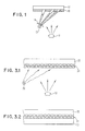
- Fig. 1 the one step process of metal deposition 10 (e.g. copper) from a vapor source 11 onto a substrate 12 (e.g. PMMA) with simultaneous selective ablation originating from an ablation energy source 13 directed through a mask 14 thereby providing the selectivity.
- metal deposition 10 e.g. copper
- substrate 12 e.g. PMMA
- ablation conditions are of sufficient energy fluency to prevent any metal deposition in the ablated areas.
- the two step process illustrated in Figs. 2.1 and 2.2 allows initially formed trenches 20a in polymer 20 (e.g. PMMA) on substrate 19 (e.g. glass) to be filled with metal 26 (e.g. copper) as the initially unablated areas are then ablated by use of a mask 27 which is a negative of the initially used mask 21.
- Vapor source 11 and ablation energy source 13 are the same as in Fig. 1.
- the trenches are formed by ablation of sufficient energy fluency and in the second step the ablation is of sufficient energy fluency to selectively prevent metal deposition.
- This process allows filling of "gapless" trenches with condensing metal while preventing overhang of the metal and may be referred to as planerization. Stated otherwise, planerization occurs when the trenches 20a are filled with metal 26 so that polymer 20 and metal 26 have a surface that lies in the same outer plane, i.e. the plane facing vapor source 11.
- the illustrated technique of Figs. 3.1 and 3.2 utilizes low intensity ablation energy source 30 initially so that an intermixed layer 31 of substrate 33 (e.g. PMMA) and metal 35 (e.g. copper) is formed as metal produced at the vapor source 32 is simultaneously deposited. After a sufficient thickness of the intermixed layer is formed, the ablation source is turned off and the metal is allowed to deposit thereby resulting in a final product 35 of metal on a substrate wherein adhesion has been enhanced by the intermediate intermixed layer.
- substrate 33 e.g. PMMA
- metal 35 e.g. copper
- Fig. 2.3 shows a "broad beam” process wherein a substrate 190 comprising glass having a polymer 200 (PMMA) with pre-formed openings 200a is exposed to a vapor source 110 (e.g. copper) simultaneously with an ablation energy source 130.
- a vapor source 110 e.g. copper
- a metal 260 such as copper is deposited in openings 200a.
- the ablation energy is not employed to form the pattern.
- the pre-formed pattern may be produced by any art-known method such as by mechanically removing portions of the PMMA film.
- an excimer laser was used as the ablation source.
- Photons with an energy of 6.42 eV (193 nm wavelength) were pulsed at a repetition rate of 1 Hz of and energy density of 0.12 joules per square centimeter per pulse.
- Copper was vapor deposited at a rate of 1.5 nm/sec onto a PMMA (polymethyl methacrylate) substrate. Copper is deposited where the opaque areas of the mask are imaged. There is no deposition where the PMMA is ablated.
- a mercury fluorescence light was used as the ablation source.
- the continuous energy density at the substrate is 0.0018 joules per square centimeter.
- Copper was deposited at a rate of 0.0005 nm/sec. on the same substrate as in example 2.
Landscapes
- Chemical & Material Sciences (AREA)
- Engineering & Computer Science (AREA)
- Organic Chemistry (AREA)
- Materials Engineering (AREA)
- Mechanical Engineering (AREA)
- Metallurgy (AREA)
- Chemical Kinetics & Catalysis (AREA)
- Health & Medical Sciences (AREA)
- Toxicology (AREA)
- Manufacturing & Machinery (AREA)
- Microelectronics & Electronic Packaging (AREA)
- Physical Vapour Deposition (AREA)
- Electrodes Of Semiconductors (AREA)
- Manufacturing Of Printed Wiring (AREA)
Applications Claiming Priority (2)
| Application Number | Priority Date | Filing Date | Title |
|---|---|---|---|
| US89918986A | 1986-08-21 | 1986-08-21 | |
| US899189 | 1986-08-21 |
Publications (2)
| Publication Number | Publication Date |
|---|---|
| EP0260410A2 true EP0260410A2 (de) | 1988-03-23 |
| EP0260410A3 EP0260410A3 (de) | 1989-03-08 |
Family
ID=25410594
Family Applications (1)
| Application Number | Title | Priority Date | Filing Date |
|---|---|---|---|
| EP87110752A Withdrawn EP0260410A3 (de) | 1986-08-21 | 1987-07-24 | Verfahren zur selektiven Ablagerung bei physikalischer Dampfabscheidung (PVD) |
Country Status (2)
| Country | Link |
|---|---|
| EP (1) | EP0260410A3 (de) |
| JP (1) | JPS6353254A (de) |
Cited By (3)
| Publication number | Priority date | Publication date | Assignee | Title |
|---|---|---|---|---|
| EP0364259A3 (de) * | 1988-10-13 | 1990-10-24 | Xerox Corporation | Verfahren zur thermischen Strukturierung von Halbleitersubstraten |
| WO1991003834A1 (en) * | 1989-09-05 | 1991-03-21 | Mcnc | Method for selectively depositing material on substrates |
| US7223444B2 (en) | 2000-05-04 | 2007-05-29 | Qunano Ab | Particle deposition apparatus and methods for forming nanostructures |
Families Citing this family (2)
| Publication number | Priority date | Publication date | Assignee | Title |
|---|---|---|---|---|
| JP2536604B2 (ja) * | 1988-10-20 | 1996-09-18 | 日立電線株式会社 | 銅・有機絶縁膜配線板の製造方法 |
| JP2983481B2 (ja) * | 1996-12-11 | 1999-11-29 | 日東電工株式会社 | プリント基板の製造方法 |
Family Cites Families (5)
| Publication number | Priority date | Publication date | Assignee | Title |
|---|---|---|---|---|
| JPS57188673A (en) * | 1981-05-14 | 1982-11-19 | Toshiba Corp | Formation of thin film by vacuum |
| JPH0817154B2 (ja) * | 1983-11-07 | 1996-02-21 | 株式会社日立製作所 | イオンビーム装置 |
| JPS6129592A (ja) * | 1984-07-20 | 1986-02-10 | Nippon Telegr & Teleph Corp <Ntt> | 二次元光学用パタ−ンの形成方法 |
| JPS61108195A (ja) * | 1984-11-01 | 1986-05-26 | インタ−ナショナル ビジネス マシ−ンズ コ−ポレ−ション | 基板上に電気的に連続した層を形成する方法 |
| US4626315A (en) * | 1984-11-09 | 1986-12-02 | Fuji Photo Film Co., Ltd. | Process of forming ultrafine pattern |
-
1987
- 1987-05-15 JP JP62117260A patent/JPS6353254A/ja active Pending
- 1987-07-24 EP EP87110752A patent/EP0260410A3/de not_active Withdrawn
Cited By (3)
| Publication number | Priority date | Publication date | Assignee | Title |
|---|---|---|---|---|
| EP0364259A3 (de) * | 1988-10-13 | 1990-10-24 | Xerox Corporation | Verfahren zur thermischen Strukturierung von Halbleitersubstraten |
| WO1991003834A1 (en) * | 1989-09-05 | 1991-03-21 | Mcnc | Method for selectively depositing material on substrates |
| US7223444B2 (en) | 2000-05-04 | 2007-05-29 | Qunano Ab | Particle deposition apparatus and methods for forming nanostructures |
Also Published As
| Publication number | Publication date |
|---|---|
| JPS6353254A (ja) | 1988-03-07 |
| EP0260410A3 (de) | 1989-03-08 |
Similar Documents
| Publication | Publication Date | Title |
|---|---|---|
| US4574095A (en) | Selective deposition of copper | |
| US5277749A (en) | Methods and apparatus for relieving stress and resisting stencil delamination when performing lift-off processes that utilize high stress metals and/or multiple evaporation steps | |
| US6035527A (en) | Method for the production of printed circuit boards | |
| US4352716A (en) | Dry etching of copper patterns | |
| US5080455A (en) | Ion beam sputter processing | |
| EP1141779B1 (de) | Verfahren zur photolackbeschichtung auf ein substrat | |
| EP0048328A2 (de) | Sublimierungsverfahren zur Herstellung eines Schichtmusters | |
| EP0260514B1 (de) | Verfahren zur photoselektiven Metallisierung | |
| EP0180101B1 (de) | Musterabsetzung durch Laserablation | |
| JP3222660B2 (ja) | 基材表面の処理方法 | |
| JPH02260492A (ja) | パターン化法及び製品 | |
| JPS6347788B2 (de) | ||
| EP0477170A1 (de) | Verfahren zur herstellung von mehrschichtigen gedruckten schaltungen | |
| US5064681A (en) | Selective deposition process for physical vapor deposition | |
| EP0536376B1 (de) | Verfahren zur herstellung einer heimschicht für selektive metallbeschichtung | |
| JPH04505481A (ja) | 被覆方法 | |
| US5750212A (en) | Process for the deposition of structured metallic coatings on glass substrates | |
| US6248958B1 (en) | Resistivity control of CIC material | |
| US5225251A (en) | Method for forming layers by UV radiation of aluminum nitride | |
| JPS6353254A (ja) | 乾式付着方法 | |
| CA1225363A (en) | Process for depositing metallic copper | |
| JPH04263490A (ja) | 薄膜回路の製造方法 | |
| US4555460A (en) | Mask for the formation of patterns in lacquer layers by means of X-ray lithography and method of manufacturing same | |
| US5028306A (en) | Process for forming a ceramic-metal adduct | |
| US6998346B2 (en) | Method for the patterned, selective metallization of a surface of a substrate |
Legal Events
| Date | Code | Title | Description |
|---|---|---|---|
| PUAI | Public reference made under article 153(3) epc to a published international application that has entered the european phase |
Free format text: ORIGINAL CODE: 0009012 |
|
| AK | Designated contracting states |
Kind code of ref document: A2 Designated state(s): DE FR GB IT |
|
| 17P | Request for examination filed |
Effective date: 19880616 |
|
| PUAL | Search report despatched |
Free format text: ORIGINAL CODE: 0009013 |
|
| AK | Designated contracting states |
Kind code of ref document: A3 Designated state(s): DE FR GB IT |
|
| 17Q | First examination report despatched |
Effective date: 19910318 |
|
| STAA | Information on the status of an ep patent application or granted ep patent |
Free format text: STATUS: THE APPLICATION IS DEEMED TO BE WITHDRAWN |
|
| 18D | Application deemed to be withdrawn |
Effective date: 19940201 |
|
| RIN1 | Information on inventor provided before grant (corrected) |
Inventor name: BERRY, CHRISTOPHER JOHN Inventor name: YEE, DENNIS SEK-ON Inventor name: GUARNIERI, RICHARD C. Inventor name: CUOMO, JEROME JOHN |