EP0260476A2 - Lasers planaires monolithiquement intégrés de longueurs d'onde d'émission différentes et leurs procédés de préparation - Google Patents
Lasers planaires monolithiquement intégrés de longueurs d'onde d'émission différentes et leurs procédés de préparation Download PDFInfo
- Publication number
- EP0260476A2 EP0260476A2 EP87112177A EP87112177A EP0260476A2 EP 0260476 A2 EP0260476 A2 EP 0260476A2 EP 87112177 A EP87112177 A EP 87112177A EP 87112177 A EP87112177 A EP 87112177A EP 0260476 A2 EP0260476 A2 EP 0260476A2
- Authority
- EP
- European Patent Office
- Prior art keywords
- substrate
- gallium
- aluminum
- lasing
- arsenide
- Prior art date
- Legal status (The legal status is an assumption and is not a legal conclusion. Google has not performed a legal analysis and makes no representation as to the accuracy of the status listed.)
- Withdrawn
Links
Images

Classifications
-
- H—ELECTRICITY
- H01—ELECTRIC ELEMENTS
- H01S—DEVICES USING THE PROCESS OF LIGHT AMPLIFICATION BY STIMULATED EMISSION OF RADIATION [LASER] TO AMPLIFY OR GENERATE LIGHT; DEVICES USING STIMULATED EMISSION OF ELECTROMAGNETIC RADIATION IN WAVE RANGES OTHER THAN OPTICAL
- H01S5/00—Semiconductor lasers
- H01S5/40—Arrangement of two or more semiconductor lasers, not provided for in groups H01S5/02 - H01S5/30
- H01S5/4025—Array arrangements, e.g. constituted by discrete laser diodes or laser bar
- H01S5/4031—Edge-emitting structures
-
- H—ELECTRICITY
- H01—ELECTRIC ELEMENTS
- H01S—DEVICES USING THE PROCESS OF LIGHT AMPLIFICATION BY STIMULATED EMISSION OF RADIATION [LASER] TO AMPLIFY OR GENERATE LIGHT; DEVICES USING STIMULATED EMISSION OF ELECTROMAGNETIC RADIATION IN WAVE RANGES OTHER THAN OPTICAL
- H01S5/00—Semiconductor lasers
- H01S5/02—Structural details or components not essential to laser action
- H01S5/026—Monolithically integrated components, e.g. waveguides, monitoring photo-detectors, drivers
-
- H—ELECTRICITY
- H01—ELECTRIC ELEMENTS
- H01S—DEVICES USING THE PROCESS OF LIGHT AMPLIFICATION BY STIMULATED EMISSION OF RADIATION [LASER] TO AMPLIFY OR GENERATE LIGHT; DEVICES USING STIMULATED EMISSION OF ELECTROMAGNETIC RADIATION IN WAVE RANGES OTHER THAN OPTICAL
- H01S5/00—Semiconductor lasers
- H01S5/04—Processes or apparatus for excitation, e.g. pumping, e.g. by electron beams
- H01S5/042—Electrical excitation ; Circuits therefor
- H01S5/0421—Electrical excitation ; Circuits therefor characterised by the semiconducting contacting layers
- H01S5/0422—Electrical excitation ; Circuits therefor characterised by the semiconducting contacting layers with n- and p-contacts on the same side of the active layer
-
- H—ELECTRICITY
- H01—ELECTRIC ELEMENTS
- H01S—DEVICES USING THE PROCESS OF LIGHT AMPLIFICATION BY STIMULATED EMISSION OF RADIATION [LASER] TO AMPLIFY OR GENERATE LIGHT; DEVICES USING STIMULATED EMISSION OF ELECTROMAGNETIC RADIATION IN WAVE RANGES OTHER THAN OPTICAL
- H01S5/00—Semiconductor lasers
- H01S5/20—Structure or shape of the semiconductor body to guide the optical wave ; Confining structures perpendicular to the optical axis, e.g. index or gain guiding, stripe geometry, broad area lasers, gain tailoring, transverse or lateral reflectors, special cladding structures, MQW barrier reflection layers
- H01S5/22—Structure or shape of the semiconductor body to guide the optical wave ; Confining structures perpendicular to the optical axis, e.g. index or gain guiding, stripe geometry, broad area lasers, gain tailoring, transverse or lateral reflectors, special cladding structures, MQW barrier reflection layers having a ridge or stripe structure
- H01S5/2201—Structure or shape of the semiconductor body to guide the optical wave ; Confining structures perpendicular to the optical axis, e.g. index or gain guiding, stripe geometry, broad area lasers, gain tailoring, transverse or lateral reflectors, special cladding structures, MQW barrier reflection layers having a ridge or stripe structure in a specific crystallographic orientation
-
- H—ELECTRICITY
- H01—ELECTRIC ELEMENTS
- H01S—DEVICES USING THE PROCESS OF LIGHT AMPLIFICATION BY STIMULATED EMISSION OF RADIATION [LASER] TO AMPLIFY OR GENERATE LIGHT; DEVICES USING STIMULATED EMISSION OF ELECTROMAGNETIC RADIATION IN WAVE RANGES OTHER THAN OPTICAL
- H01S5/00—Semiconductor lasers
- H01S5/20—Structure or shape of the semiconductor body to guide the optical wave ; Confining structures perpendicular to the optical axis, e.g. index or gain guiding, stripe geometry, broad area lasers, gain tailoring, transverse or lateral reflectors, special cladding structures, MQW barrier reflection layers
- H01S5/22—Structure or shape of the semiconductor body to guide the optical wave ; Confining structures perpendicular to the optical axis, e.g. index or gain guiding, stripe geometry, broad area lasers, gain tailoring, transverse or lateral reflectors, special cladding structures, MQW barrier reflection layers having a ridge or stripe structure
- H01S5/227—Buried mesa structure ; Striped active layer
- H01S5/2275—Buried mesa structure ; Striped active layer mesa created by etching
-
- H—ELECTRICITY
- H01—ELECTRIC ELEMENTS
- H01S—DEVICES USING THE PROCESS OF LIGHT AMPLIFICATION BY STIMULATED EMISSION OF RADIATION [LASER] TO AMPLIFY OR GENERATE LIGHT; DEVICES USING STIMULATED EMISSION OF ELECTROMAGNETIC RADIATION IN WAVE RANGES OTHER THAN OPTICAL
- H01S5/00—Semiconductor lasers
- H01S5/40—Arrangement of two or more semiconductor lasers, not provided for in groups H01S5/02 - H01S5/30
- H01S5/4025—Array arrangements, e.g. constituted by discrete laser diodes or laser bar
- H01S5/4087—Array arrangements, e.g. constituted by discrete laser diodes or laser bar emitting more than one wavelength
-
- Y—GENERAL TAGGING OF NEW TECHNOLOGICAL DEVELOPMENTS; GENERAL TAGGING OF CROSS-SECTIONAL TECHNOLOGIES SPANNING OVER SEVERAL SECTIONS OF THE IPC; TECHNICAL SUBJECTS COVERED BY FORMER USPC CROSS-REFERENCE ART COLLECTIONS [XRACs] AND DIGESTS
- Y10—TECHNICAL SUBJECTS COVERED BY FORMER USPC
- Y10S—TECHNICAL SUBJECTS COVERED BY FORMER USPC CROSS-REFERENCE ART COLLECTIONS [XRACs] AND DIGESTS
- Y10S438/00—Semiconductor device manufacturing: process
- Y10S438/956—Making multiple wavelength emissive device
Definitions
- This invention is directed to semiconductor lasers, specifically monolithically integrated lasers, and to processes for their manufacture.
- planar surfaces i.e., surfaces having the low level of relief common to semiconductor devices fabricated using planar processing. Planar surfaces exhibit a relief variance of a micrometer ( ⁇ m) or less.
- a laser can be formed by planar processing. Such lasers are formed by introducing along a substrate surface N and P conductivity type ions in laterally spaced regions so that an active region is created therebetween. While such lasers are ideal in terms of achieving an overall planar surface for a chip, emission efficiency of such lasers is relatively low.
- Botez "Laser Diodes are Power-Packed", IEEE Spectrum, June 1985, pp. 43-53, provides a state of the art survey of such laser diodes as discrete elements. Positive index lasers are disclosed and schematically illustrated. Lasers can be formed with only three superimposed layers, superimposed N and P conductivity type cladding layers with an active layer intervening. Efficient lasers are typically formed with five or more superimposed layers. Botez discusses only discrete lasers and monolithically integrated laser arrays emitting at a single wavelength.
- Mito et al U.S. Patent 4,318,058 discloses laterally related lasers integrated on a common chip capable of emitting at differing wavelengths.
- Mito et al deposits III-V compound layers on a substrate by molecular beam epitaxy while varying the III-V compound composition during an electron beam sweep across the substrate surface.
- An inherent disadvantage of the Mito et al process is that molecular beam deposition is slow as compared to organometallic vapor epitaxial deposition.
- the disadvantage of the Mito et al structure produced is that one lasing region as initially formed grades smoothly into the next laterally adjacent lasing region.
- Mito et al discloses a III-V compound laser formed using arsenic as group V ions and aluminum and gallium as group III ions in which adjacent lasing regions are separated by etch troughs.
- the overall topography of the chip is a mesa topography rather than a planar topography.
- Mito et al discloses an alternative planar construction using indium as group III ions and phosphorus as group V ions and resorting to implanting proton radiation insulated regions for isolation in the epitaxy between adjacent lasers.
- no substrate surface between adjacent lasers is available for integration of other, non-laser chip components.
- the highly doped proton radiation insulated regions are, of course, poorly suited to serving as fabrication areas for many types of circuit components.
- It is one object of this invention to provide a process of preparing monolithically integrated lasers capable of emitting at differing wavelengths comprising providing a substrate, providing superimposed N and P conductivity type cladding layers separated by an active layer at laterally spaced lasing regions on the substrate, the substrate and the layers together forming a monocrystalline III-V compound structure, wherein the group V ions are arsenic and the group III ions are at least one of gallium and aluminum, and the active layers at two of the lasing regions differ to generate emissions at differing wavelengths; such process being capable of offering the advantage of selective deposition of the waveguiding III-V compound at desired sites.
- Additional advantages which can be realized include forming waveguides with planar surfaces, avoiding etching of large areas of the device or epitaxial deposition onto other areas after the waveguide is formed in order to achieve the desired planar surface structure.
- the above advantages can be realized while at the same time choosing the initial composition of the substrate to achieve desired positive index waveguide and electrical isolation characteristics.
- the process is characterized in that at least two positive index guided lasing regions capable of emitting at differing wavelengths presenting with the substrate a planar surface of the monocrystalline III-V compound structure are formed by (a) providing a substrate having adjacent one major surface monocrystalline gallium aluminum arsenide having a resistivity greater than 105 ohm-cm, (b) providing on the one major surface a protective layer defining a first opening, (c) through the first opening creating a channel in the substrate to expose an unprotected portion of the substrate beneath the one major surface, (d) epitaxially depositing on only the unprotected portion of the substrate a first lasing region comprised of the superimposed N and P conductivity type cladding layers separated by the active layer, the active layer being of a higher refractive index than the substrate monocrystalline gallium aluminum arsenide, (e) terminating epitaxial deposition when the first lasing region forms with the one major
- a further advantage is that the substrate portion separating the lasing regions along the planar surface requires no special modification to isolate adjacent layers and provide positive waveguiding. Another advantage is that the substrate adjacent the planar surface is better suited for
- the monolithically integrated lasers are characterized in that the substrate forms with the two lasing regions a planar surface of the monocrystalline III-V compound structure and the substrate comprises monocrystalline gallium aluminum arsenide of a single conductivity type having a resistivity of greater than 105 ohm-cm laterally separating the two lasing regions and providing positive index wave guiding at its interface with the two active layers.
- Figure 1 a detail of an exemplary preferred semiconductor device 100 according to the present invention containing two monolithically integrated lasers capable of emission at differing wavelengths.
- the device in the detail shown is comprised of a monocrystalline III-V compound structure consisting of a substrate 102 and a laterally spaced first and second lasing regions 108 and 208 epitaxially grown in channels 110 and 210, respectively, of the substrate.
- a first major surface 124 of the substrate and the upper surface of the lasing regions together form an overall planar surface of the device while the substrate alone forms a second major surface 126 of the device.
- a first electrode 128 serves as an ohmic contact to the second major surface.
- An insulative layer 130 overlies the planar surface bridging the isolating portion of the substrate and the lasing regions and forms first and second apertures 132 and 232 overlying the first and second las ing regions.
- a second and third electrodes 134 and 234 contact the upper surfaces of the first and second lasing regions within the first and second apertures, respectively, and also each laterally traverse at least a portion of the insulative layer.
- an electrically insulative barrier layer 136 Overlying the second and third electrodes and the insulative layer is an electrically insulative barrier layer 136.
- the electrodes and the insulative and barrier layers can be of any convenient conventional composition. Both gold-zinc alloys and titanium nitride are typical electrode materials.
- the insulative barrier layer is entirely optional, since the device can be mounted in a hermetically sealed housing, if desired.
- the barrier layer can take the form of a passivating layer, such as a borosilicate glass.
- the insulative layer can take the form of a chemically vapor deposited insulative material, such as silica or silicon nitride. Additional conductive and/or insulative layers, not shown, can overlie the barrier layer, depending upon the requirements of other, optional device components, not shown.
- the substrate 102 in one preferred form is comprised of a more conductive portion 104 typically formed of gallium arsenide containing at least 5 X 10¹⁷ and preferably from 1 to 3 X 10¹⁸ N conductivity type ions per cubic centimeter.
- An isolating portion 106 of the substrate is comprised of an aluminum gallium arsenide layer epitaxially grown on the more conductive portion of the substrate.
- the isola ting portion contains sufficient aluminum to reduce its refractive index below that of the active layers of the lasing regions, which it laterally confines, so that it forms with each of the lasing regions a positive index waveguide.
- the isolating portion preferably contains about 30 to 60 mole percent aluminum, mole percentages being based on the total group III ions present, except as otherwise indicated.
- at least the portion of the substrate adjacent the first major surface exhibits a resistivity of greater than 105 ohm-cm, preferably greater than 107 ohm-cm.
- Suitable resistivity levels can be achieved by known gallium arsenide deposition techniques, such as by gallium arsenide deposition at temperatures of 550 to 650°C and/or in an atmosphere containing from 2 to 10 ppm of oxygen. Since the insulating portion need not be relied upon for current conduction, the majority charge carriers can be of either N or P conductivity type or the insulating portion can be substantially intrinsic.
- the substrate portion adjacent the first major surface is particularly suited to the placement of additional, optional circuit components, desired.
- the isolating portion 106a laterally separating the lasing regions is a particularly suitable site for additional, optional circuit components, such as additional semi-conductive elements.
- the lasing regions lying entirely within the channels formed by the substrate, have their lateral extent defined by the isolating portion of the substrate and their lower walls 112 and 212 defined by the more conductive portion of the substrate. Adjacent the lower channel wall the lasing regions are shown comprised of gallium arsenide lower capping layers 114 and 214, respectively, typically having an N type conductivity ion concentration of from 1017 to 5 X 10¹⁸ ions per cubic centimeter. Lying immediately above the lower capping layers are lower cladding layers 116 and 216 of N conductivity type. Lying above the lower cladding layers are upper cladding layers 118 and 218 of P conductivity type.
- Each cladding layer can be comprised of aluminum arsenide or gallium aluminum arsenide containing up to 90 mole percent gallium.
- the cladding layers each typically have a conductivity imparting ion concentration of from 1016 to 1018 ions per cubic centimeter, but typically each contain a somewhat lower conductivity imparting ion concentration than the capping layer with which it is in contact.
- Interposed between the upper and lower cladding layers are active layers 120 and 220.
- the active layers each normally contains a lower conductivity imparting ion concentration than either of the cladding layers it contacts. That is, each cladding layer normally contains less than 1018 conductivity imparting ions per cubic centimeter and can be as nearly intrinsic as can be conveniently realized. Additionally, each active layer contains less aluminum than either of the cladding layers it contacts and less aluminum than the isolating portion of the substrate.
- the active layers To cause the first and second lasing regions to emit at differing wavelengths their active layers must differ. It is well known that differing group III ion concentrations of active layers can shift the wavelength of emission. For example, reductions of aluminum concentration in active layers of gallium aluminum arsenide shifts emission to longer wavelengths. It is also known that thinning an active layer reduces its wavelength of emission. Either or both of these parameters of the active layers can be varied to create the desired differences in emission wavelengths.
- Capping layers 122 and 222 are in contact with the upper cladding layers 118 and 218, respectively.
- the upper capping layers are preferably comprised of gallium arsenide having a P type conductivity imparting ion concentration of greater than 1019 ions per cubic centimeter.
- the upper surface of the upper capping layers lie along the planar surface of the semiconductor device within a ⁇ m and typically within about 3000 Angstroms of the plane of the first major surface of the substrate. As shown the first major surface of the substrate and the upper surfaces of the capping layers are in their ideal, coplanar relationship.
- a monocrystalline gallium arsenide wafer is provided having properties corresponding to those of the conductive portion 104 of the substrate.
- the wafer thickness is chosen to make efficient use of material while permitting manipulation during processing without damage. While in practice a plurality of identical semiconductive devices are formed in laterally offset relation on a single wafer, the description which follows is in terms of forming a single device, since the process steps are the same.
- the isolating portion is typically grown to a thickness of from about 3 to 10 ⁇ m, optimally from about 4 to 8 ⁇ m. Formation of the substrate can be achieved by any convenient conventional means.
- a protective layer 140 is formed on the first major surface 124 of the isolating portion 106 of the substrate 102.
- the protective layer forming material can be selected from among a variety of known materials which are stable at required processing temperatures and which can be readily removed in at least selected areas. Examples of such materials are silica (SiO2), silicon nitride (Si3N4), and refractory metals as well as their oxides and silicides-e.g., tungsten, tungsten oxide, and tungsten silicide.
- the layer need be no thicker than is required to assure pin hole free coverage of the first major surface and in any event is less than about 3000 Angstroms in thickness, preferably from about 500 to 2000 Angstroms in thickness.
- the protective layer overlies the entire first major surface.
- an opening 142 is first formed in the protective layer, and the substrate is then etched through the opening to form the channel 110.
- the opening in the protective layer can be formed by conventional photomasking and etching steps.
- the protective layer can be overcoated with a layer of a conventional photoresist, imagewise exposed, and developed to define an opening in the photoresist layer corresponding to the location of the opening in the protective layer desired.
- the protective layer can then be etched through the openings in the photomask to define the desired openings.
- suitable conventional etching techniques are known, as illustrated by the various etching techniques outlined in Sugishima et al U.S. Patent 4,352,724.
- washing step After every material removal step, regard severelyless of whether the material being removed is from the substrate itself or an associated conductive or insulative layer, it is conventional practice to follow up immediately with a washing step to assure maintenance of the high levels of cleanliness required for successful semiconductor device yields. Typically deionized water is used for washing. To avoid repetitive references to washing, it is to be understood that a washing step, though not specifically described, preferably follows each step calling for removal of any material, particularly any step calling for material removal by etching.
- the protective layer is comparatively thin, it is normally immaterial whether isotropic or anisotropic etching conditions are employed to form the opening. The same comment does not apply to forming the channel.
- the side walls of the channel are shown to be perpendicular to the first major surface of the substrate. However, alternative orientations are possible and can be employed to advantage. To appreciate the alternatives some appreciation of the substrate crystal structure is required.
- the Group III-V compounds which form the substrate and lasing regions all form essentially similar cubic crystal lattices of the zinc blende type, and their lattice constants are essentially similar-e.g., 5.63 Angstroms for gallium arsenide and 5.66 Angstroms for aluminum arsenide.
- the common crystalline class and the close similarity in lattice spacings facilitates epitaxial deposition of materials differing in the selection of aluminum or gallium as the Group III ions.
- the major surfaces of the substrate lie in ⁇ 100 ⁇ crystallographic planes.
- the substrate can be etched essentially isotropically through the opening in the protective layer, with a certain amount of undercutting of the protective layer occurring.
- anisotropic etching can be achieved which reduces undercutting of the protective layer.
- Under anisotropic etching conditions the lateral walls of the channel are defined by the more thermodynamically stable crystallographic planes of the crystal structure.
- the ⁇ 111 ⁇ crystallographic planes are the most stable and can be revealed selectively by anisotropic etching to form the side walls of the channel. Any conventional anisotropic etchant can be employed.
- One preferred anisotropic etchant capable of efficiently revealing ⁇ 111 ⁇ channel side walls is a 5:1:1 volume ratio mixture of H2O:H2SO4:H2O2.
- Another suitable anisotropic etchant is a 2 percent by weight bromine dissolved in methanol.
- Figure 3A illustrates the channel side walls which result when the channel longitudinal axis is oriented parallel to one set of ⁇ 110> vectors on the ⁇ 100 ⁇ crystallographic plane forming the first major surface
- Figure 3B illustrates the channel side walls which result when the channel longitudinal axis is oriented parallel to a second set of ⁇ 110> vectors on the ⁇ 100 ⁇ crystallographic plane forming the first major surface, where the two sets of ⁇ 110> vectors are mutually perpendicular.
- the direction of ⁇ 110> vectors on a ⁇ 100 ⁇ crystal surface can be determined by light diffraction patterns on the crystal surface, as is well understood.
- discrimination between the two sets of ⁇ 110> vectors for purposes of choosing the side wall orientation of the channel created by etching requires a trial etching step in an expendable area of the substrate wafer being processed.
- FIG 3A a structure is shown similar to the right hand portion of Figure 2, with like elements assigned like reference numbers.
- the difference in the Figure 3A structure is the configuration of the channel 110a.
- the channel is formed by two opposed side walls 144a and 144b and a bottom wall 144c.
- the bottom wall is shown lying along the interface of the substrate portions 104 and 106-i.e., in a ⁇ 100 ⁇ crystallographic plane.
- the side walls diverge linearly from the protective layer opening toward the substrate portion 104 and then curve back to join the bottom wall.
- the linear portion of each side wall lies in a different ⁇ 111 ⁇ crystallographic plane.
- Dashed line 146 shows the lower boundary of the channel at an intermediate stage of etching.
- the regions 148a and 148b are not normally removed by etching, but should be removable if the rate of etching along the bottom wall is slowed, as by introducing an etch resistant layer in the substrate during its formation.
- the rounding of the channel side walls at their intersection with the bottom wall is advantageous in that the necessity of epitaxy at the areally constricted oblique intersections of the ⁇ 111 ⁇ and ⁇ 100 ⁇ planes is avoided, thereby facilitating epitaxy on all channel walls.
- FIG. 3B a somewhat broader opening 142a is shown, since the side walls 150a and 150b of the channel 110b converge toward the channel bottom wall 152.
- Dashed line 154 represents the bottom wall at an intermediate stage of etching. It is to be noted that in this instance side walls entirely conform to ⁇ 111 ⁇ crystallographic planes and that the angles of intersection of the side walls and the bottom wall are obtuse, which facilitates epitaxial deposition at the intersections of the ⁇ 100 ⁇ and ⁇ 111 ⁇ crystallographic planes.
- a suitable etchant choice it should be possible to form a channel with side walls lying in ⁇ 110 ⁇ crystallographic planes and a bottom wall lying in a ⁇ 110 ⁇ crystallographic plane.
- the substrate surfaces formed by ⁇ 110 ⁇ crystallographic planes are more thermodynamically stable during etching than the surfaces formed by ⁇ 100 ⁇ crystallographic planes.
- etching would be expected to proceed anisotropically, deepening the channel bottom wall while exhibiting little undercutting of the protective layer.
- the next step is to deposit epitaxially III-V compound selectively in the channel formed so that deposition occurs only in the channel and not on the protective layer.
- epitaxially III-V compound selectively in the channel formed so that deposition occurs only in the channel and not on the protective layer.
- a preferred procedure for depositing III-V compound only on the unprotected or exposed surfaces of the substrate lying in the channel employs selected conditions of organometallic vapor phase epitaxy.
- the substrate in any one of the forms shown in Figures 2, 3A, or 3B is placed in a vacuum chamber where it is heated to a temperature in the range of from 500 to 800°C, preferably in the range of from 650 to 750°C.
- the pressure in the vacuum chamber is reduced to less than 50 torr., preferably less than 10 torr.
- an atmosphere is provided in the vacuum chamber comprised of arsine (AsH3) and one or a mixture of organo-aluminum and organo-gallium gases-e.g., trimethyl or triethyl aluminum or gallium.
- the aluminum and gallium ratio are dictated by the ratio of these metals desired in the epitaxy being deposited on the substrate.
- a molar excess of the arsine gas is maintained.
- a molar ratio of vapor phase arsine to total vapor phase aluminum and gallium of from about 2:1 to 100:1 is maintained.
- Deposition is continued until the epitaxy deposited in the channel forms with the first major surface of the substrate an overall planar surface-i.e., until the surface of the epitaxy in the lasing region lies within about a ⁇ m of the first major surface of the substrate, preferably within about 3000 Angstroms of the first major surface.
- N or P dopant materials are introduced into the vacuum chamber as vapor phase compounds along with the other gases.
- N type dopants such as silicon, selenium, sulfur, tellurium, tin, and germanium
- vapor phase compounds such as silane, hydrogen selenide, germanium hydride, dialkyl telluride, or tetraalkyl tin
- P type dopants such zinc, cadmium, beryllium, and magnesium, can be introduced as the corresponding dialkyl compounds, where alkyl in each instance is independently methyl or ethyl.
- doping procedures can generally follow the conventional practices of the art.
- edge contouring of the successive epitaxially deposited layers is observed, the contouring effect is not incompatible with obtaining the desired final planar surface configuration. Since contouring results from interaction with the substrate channel walls, once epitaxy covers these walls, the successive deposition favors restoring planarity to the upper surface of the epitaxy. Edge contours of lasing region layers can be minimized by maintaining the channel depth small in relation to its width. Where the channel is initially bounded by side walls lying in ⁇ 110 ⁇ crystallographic planes, the slower deposition onto walls of this crystallographic orientation favors the deposition of flat layers essentially free of edge contours, as shown in Figure 1.
- the lasing region epitaxy is grown just to or slightly below the first major surface of the substrate to form a planar surface extension of the first major surface-i.e., a surface that lies within about a ⁇ m and preferably within about 3000 Angstroms of the first major surface.
- a planar surface extension of the first major surface i.e., a surface that lies within about a ⁇ m and preferably within about 3000 Angstroms of the first major surface.
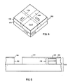
- the next objective to prevent further III-V compound epitaxy at this location while forming the second lasing region is achieved merely by closing the opening 142 with additional material of the type used to form the protective layer 140. This can be done locally over the first lasing region or uniformly over the entire upper surface of the device. It is preferred first to remove the entire protective layer 140 and then, as shown in Figure 5, to form a second protective layer 156 over the entire first major surface 124 of the substrate and the capping layer of the first lasing region. Thereafter opening 158 and channel 210 are formed similarly as described above with reference to opening 142 and channel 110.
- the layers of the second lasing region 208 can then be epitaxially grown selectively in the channel 210.
- the layers of the second lasing region 208 can be similar to those of first lasing region, differing only by the active layer difference required to shift emission of the second lasing region with respect to emission of the first lasing region.
- the layers of the second lasing region can differ in number, thickness, and composition from those of the first lasing region, although they are selected from among the same general preferred parameter ranges noted above in discussing the first lasing region layers.
- the protective layer or layers used for directing epitaxy can remain as permanent layers of the completed device or can be removed and replaced by an insulative layer, such as layer 130 in Figure 1. Alternately, the insulative and protective layers can be used together. It is to be noted that the insulative layer 130 as shown in Figure 1 covers portions of the lasing regions to limit the lateral contact of the second and third electrodes with the lasing regions. This arrangement can be used to advantage to combine gain guiding with positive index guiding.
- the substrate containing the lasing regions intended to form the semiconductive device is typically cleaved from a wafer of which it forms a part during fabrication so that two parallel smooth mirror edges intersect the channels containing the lasing regions. These mirror edges interact with the lasing regions to increase the emission efficiency of the completed device.
- the lasing regions contain five separate layers as shown in Figure 1. Any one or combination of the four capping layers 114, 214, 122, and 222 shown in Figure 1 can be omitted, the capping layers 114 and 214 being generally less determinative of overall performance than the capping layers 122 and 222.
- waveguides other than lasers can be formed in one or more channels using procedures essentially similar to those previously described.
- a simple, non-lasing waveguide can be formed according to the process of this invention merely by epitaxially depositing in a channel a single III-V compound.
- the III-V compound can take any one of the forms described above for the various laser layers, but preferably the positive index relationship is maintained for waveguiding efficiency.
- the substrate 102 has been shown to be comprised of both conductive portion 104 and isolating portion 106; however, only the isolating portion is essential.
- a unitary substrate can be formed in which a wafer having the composition of the isolating portion is provided and etched to form channels therein without any intervening step of epitaxially deposition additional III-V compound thereon.
Landscapes
- Physics & Mathematics (AREA)
- Condensed Matter Physics & Semiconductors (AREA)
- General Physics & Mathematics (AREA)
- Electromagnetism (AREA)
- Optics & Photonics (AREA)
- Semiconductor Lasers (AREA)
Applications Claiming Priority (2)
| Application Number | Priority Date | Filing Date | Title |
|---|---|---|---|
| US908758 | 1986-09-18 | ||
| US06/908,758 US4888085A (en) | 1986-09-18 | 1986-09-18 | Processes for their manufacture of monolithically integrated planar lasers differing in emission wavelengths |
Publications (2)
| Publication Number | Publication Date |
|---|---|
| EP0260476A2 true EP0260476A2 (fr) | 1988-03-23 |
| EP0260476A3 EP0260476A3 (fr) | 1988-12-28 |
Family
ID=25426209
Family Applications (1)
| Application Number | Title | Priority Date | Filing Date |
|---|---|---|---|
| EP87112177A Withdrawn EP0260476A3 (fr) | 1986-09-18 | 1987-08-21 | Lasers planaires monolithiquement intégrés de longueurs d'onde d'émission différentes et leurs procédés de préparation |
Country Status (4)
| Country | Link |
|---|---|
| US (1) | US4888085A (fr) |
| EP (1) | EP0260476A3 (fr) |
| JP (1) | JPS6387784A (fr) |
| CA (1) | CA1280197C (fr) |
Families Citing this family (7)
| Publication number | Priority date | Publication date | Assignee | Title |
|---|---|---|---|---|
| US5013682A (en) * | 1986-10-22 | 1991-05-07 | Texas Instruments Incorporated | Method for selective epitaxy using a WSI mask |
| JPS6450494A (en) * | 1987-08-20 | 1989-02-27 | Nec Corp | Multiwavelength light source semiconductor element |
| US5104824A (en) * | 1990-11-06 | 1992-04-14 | Bell Communications Research, Inc. | Selective area regrowth for surface-emitting lasers and other sharp features |
| JPH07111357A (ja) * | 1993-10-05 | 1995-04-25 | Mitsubishi Electric Corp | 半導体レーザの製造方法 |
| TWI237322B (en) * | 2004-12-14 | 2005-08-01 | Cleavage Entpr Co Ltd | Method and device by using a laser beam to cut Gallium arsenide (GaAs) epitaxy wafer |
| US8710630B2 (en) * | 2011-07-11 | 2014-04-29 | Taiwan Semiconductor Manufacturing Company, Ltd. | Mechanisms for marking the orientation of a sawed die |
| CN109906518B (zh) * | 2016-12-05 | 2022-07-01 | 歌尔股份有限公司 | 微激光二极管转移方法和微激光二极管显示装置制造方法 |
Family Cites Families (14)
| Publication number | Priority date | Publication date | Assignee | Title |
|---|---|---|---|---|
| US3579055A (en) * | 1968-08-05 | 1971-05-18 | Bell & Howell Co | Semiconductor laser device and method for it{3 s fabrication |
| US4033796A (en) * | 1975-06-23 | 1977-07-05 | Xerox Corporation | Method of making buried-heterostructure diode injection laser |
| US4318058A (en) * | 1979-04-24 | 1982-03-02 | Nippon Electric Co., Ltd. | Semiconductor diode laser array |
| JPS55165691A (en) * | 1979-06-13 | 1980-12-24 | Nec Corp | Compound semiconductor laser element |
| JPS5826834B2 (ja) * | 1979-09-28 | 1983-06-06 | 株式会社日立製作所 | 半導体レ−ザ−装置 |
| US4532694A (en) * | 1981-06-11 | 1985-08-06 | Honeywell Inc. | Method of fabricating emitter/detector-in-a-well for the integration of electronic and optoelectronic components |
| US4484332A (en) * | 1982-06-02 | 1984-11-20 | The United States Of America As Represented By The Secretary Of The Air Force | Multiple double heterojunction buried laser device |
| JPS5941317A (ja) * | 1982-08-31 | 1984-03-07 | Mitsui Toatsu Chem Inc | プロピレン―エチレンブロック共重合体の製造法 |
| US4509996A (en) * | 1982-11-05 | 1985-04-09 | International Standard Electric Corporation | Injection laser manufacture |
| US4566171A (en) * | 1983-06-20 | 1986-01-28 | At&T Bell Laboratories | Elimination of mask undercutting in the fabrication of InP/InGaAsP BH devices |
| EP0132408A3 (fr) * | 1983-07-26 | 1986-04-16 | Jim Auclair | Procédé et appareil pour faire croítre des couches ou pour produire des revêtements sur un substrat |
| US4577321A (en) * | 1983-09-19 | 1986-03-18 | Honeywell Inc. | Integrated quantum well lasers for wavelength division multiplexing |
| US4645687A (en) * | 1983-11-10 | 1987-02-24 | At&T Laboratories | Deposition of III-V semiconductor materials |
| US4660208A (en) * | 1984-06-15 | 1987-04-21 | American Telephone And Telegraph Company, At&T Bell Laboratories | Semiconductor devices employing Fe-doped MOCVD InP-based layer for current confinement |
-
1986
- 1986-09-18 US US06/908,758 patent/US4888085A/en not_active Expired - Fee Related
-
1987
- 1987-07-29 CA CA000543239A patent/CA1280197C/fr not_active Expired - Fee Related
- 1987-08-21 EP EP87112177A patent/EP0260476A3/fr not_active Withdrawn
- 1987-09-18 JP JP62234731A patent/JPS6387784A/ja active Pending
Also Published As
| Publication number | Publication date |
|---|---|
| EP0260476A3 (fr) | 1988-12-28 |
| JPS6387784A (ja) | 1988-04-19 |
| US4888085A (en) | 1989-12-19 |
| CA1280197C (fr) | 1991-02-12 |
Similar Documents
| Publication | Publication Date | Title |
|---|---|---|
| US4788159A (en) | Process for forming a positive index waveguide | |
| US5104824A (en) | Selective area regrowth for surface-emitting lasers and other sharp features | |
| US10468551B2 (en) | Light-emitter-based devices with lattice-mismatched semiconductor structures | |
| CA1276276C (fr) | Dispositifs a semiconducteur a couche epitaxiable de groupe iii-v dopee au titane | |
| US5747366A (en) | Method of fabricating a surface emitting semiconductor laser | |
| US4566171A (en) | Elimination of mask undercutting in the fabrication of InP/InGaAsP BH devices | |
| CA1151775A (fr) | Fabrication en serie de dispositifs a semi-conducteurs | |
| US5360754A (en) | Method for the making heteroepitaxial thin layers and electronic devices | |
| JPH04337689A (ja) | オプトエレクトロニクス半導体装置及びその製造方法 | |
| US4999315A (en) | Method of controlling dopant incorporation in high resistivity In-based compound Group III-V epitaxial layers | |
| JPH0864906A (ja) | 半導体装置の製法 | |
| US4661961A (en) | Buried heterostructure devices with unique contact-facilitating layers | |
| EP0261408B1 (fr) | Laser comportant des dispositifs planaires monolithiquement intégrés et leurs procédés de préparation | |
| US4503539A (en) | Semiconductor laser | |
| US5854088A (en) | Method of manufacturing a surface-emitting laser | |
| US5953581A (en) | Methods for manufacturing group III nitride compound semiconductor laser diodes | |
| US4888085A (en) | Processes for their manufacture of monolithically integrated planar lasers differing in emission wavelengths | |
| EP1037344B1 (fr) | Hétérostructure enterrée pour laser et diodes électroluminicentes | |
| US5478774A (en) | Method of fabricating patterned-mirror VCSELs using selective growth | |
| EP0266826A1 (fr) | Laser à semi-conducteur et son procédé de fabrication | |
| JP3424634B2 (ja) | 窒化物半導体レーザ素子 | |
| CA1282874C (fr) | Dispositifs a semiconducteur a couche epitaxiale a grande resistivite pour confiner le courant | |
| US4665525A (en) | Means for a self-aligned multilayer laser epitaxy structure device | |
| Zhao et al. | Sub-milliampere single-quantum-well InGaAs-GaAs-AlGaAs addressable laser arrays | |
| EP0786147A2 (fr) | Utilisation d'un laser a configuration en arete dans un canal |
Legal Events
| Date | Code | Title | Description |
|---|---|---|---|
| PUAI | Public reference made under article 153(3) epc to a published international application that has entered the european phase |
Free format text: ORIGINAL CODE: 0009012 |
|
| AK | Designated contracting states |
Kind code of ref document: A2 Designated state(s): BE DE FR GB NL |
|
| PUAL | Search report despatched |
Free format text: ORIGINAL CODE: 0009013 |
|
| AK | Designated contracting states |
Kind code of ref document: A3 Designated state(s): BE DE FR GB NL |
|
| 17P | Request for examination filed |
Effective date: 19890521 |
|
| 17Q | First examination report despatched |
Effective date: 19910923 |
|
| STAA | Information on the status of an ep patent application or granted ep patent |
Free format text: STATUS: THE APPLICATION IS DEEMED TO BE WITHDRAWN |
|
| 18D | Application deemed to be withdrawn |
Effective date: 19920204 |
|
| RIN1 | Information on inventor provided before grant (corrected) |
Inventor name: SMITH, FRANK THOMAS JOHNEASTMAN KODAK COMPANY |