EP0260502A2 - Zeitstempelschaltung mit automatischer Bereichregelung - Google Patents
Zeitstempelschaltung mit automatischer Bereichregelung Download PDFInfo
- Publication number
- EP0260502A2 EP0260502A2 EP87112563A EP87112563A EP0260502A2 EP 0260502 A2 EP0260502 A2 EP 0260502A2 EP 87112563 A EP87112563 A EP 87112563A EP 87112563 A EP87112563 A EP 87112563A EP 0260502 A2 EP0260502 A2 EP 0260502A2
- Authority
- EP
- European Patent Office
- Prior art keywords
- count
- clock
- frequency
- time
- circuit
- Prior art date
- Legal status (The legal status is an assumption and is not a legal conclusion. Google has not performed a legal analysis and makes no representation as to the accuracy of the status listed.)
- Withdrawn
Links
Images



Classifications
-
- G—PHYSICS
- G06—COMPUTING OR CALCULATING; COUNTING
- G06F—ELECTRIC DIGITAL DATA PROCESSING
- G06F11/00—Error detection; Error correction; Monitoring
- G06F11/30—Monitoring
- G06F11/34—Recording or statistical evaluation of computer activity, e.g. of down time, of input/output operation ; Recording or statistical evaluation of user activity, e.g. usability assessment
- G06F11/3466—Performance evaluation by tracing or monitoring
- G06F11/348—Circuit details, i.e. tracer hardware
-
- G—PHYSICS
- G06—COMPUTING OR CALCULATING; COUNTING
- G06F—ELECTRIC DIGITAL DATA PROCESSING
- G06F11/00—Error detection; Error correction; Monitoring
- G06F11/22—Detection or location of defective computer hardware by testing during standby operation or during idle time, e.g. start-up testing
- G06F11/25—Testing of logic operation, e.g. by logic analysers
Definitions
- This invention relates generally to data acquisition systems. More particularly, this invention relates to a time measurement circuit within a data acquisition system for measuring the elapsed time between two events stored within the acquisition memory. Such event is one of a number of specified combinations of signals, such as data or instructions generated by logic within a circuit under test.
- Logic analyzers are commonly used today to analyze the. digital signals generated within a circuit.
- a logic analyzer can perform a number of functions, including acquiring and storing data generated by logic. within the circuit under test.
- One particular use of an analyzer is to monitor the instructions of a microprocessor-based circuit and the data that is generated along therewith to determine if the circuit is operating properly.
- the analyzer acts as a data acquisition system to acquire and then store data including events in memory.
- the timing of events is often critical in a circuit, and the data acquisition system typically contains a time measurement circuit for measuring the time between the events. Each event is identified or “stamped" with a unique value representing time as it is acquired, and two time values are then compared to determine the elapsed time.
- a drawback of a "stamping" technique that includes autoranging is the progressively poorer resolution (time between counts) that occurs as time progresses. Over a long time, the resolution may become less than an acceptable minimum and even fall below the rate at which events are acquired and stored. For instance, at extremely slow frequencies, successive events may be tagged with the same count. The time between these events cannot be accurately measured.
- a time stamp should maintain high resolution and yet be autoranging to increase the time over which time measurements can be made.
- An object of the invention is to provide an improved time stamp type of time measurement circuit for measuring elapsed time between specified events.
- a second object of the invention is to provide such a time measurement circuit with more accurate measurement of the elapsed time between events by improving the resolution for later-stored events.
- Another object is to provide such a time measurement circuit with autoranging.
- a further object of the invention is to implement the above measurement circuit inexpensively with commercially available logic circuits.
- a time stamp circuit for associating a time value with a specified event.
- the circuit includes means for generating a plurality of selectable clock frequencies and means for selecting the clock frequencies in decreasing order of frequency to provide a clock signal to a binary code generating means.
- the binary code generating means produces a binary code count associated as a time value with each specified event.
- control means then resets the binary count and clock frequency for the binary code generating means. In this way, the higher frequencies are employed at the beginning of the count between each pair of events, thereby maintaining a high resolution for later-stored events.
- control means and the binary code generating means in the time stamp. circuit are programmable logic arrays.
- a portion of the count of one of the counter programmable logic arrays provides the means for selecting the order of clock frequencies for the clock signal. These frequencies are provided by an oscillator connected to the time stamp circuit, whose base clock frequency is divided by frequency dividing circuitry into the plurality of slower frequencies. As the count changes, the slower frequencies are selected by the count value to extend the time over which the count is provided.
- Fig. 1 is a block diagram of a portion of a data acquisition system 10 that includes a "time stamp" type of time measurement circuit 12 embodying the invention.
- the system 10 itself may contain a number of other elements, but only those elements necessary to understand the function of the time stamp circuit 12 are shown and discussed herein.
- Target information from the circuit or device to be analyzed is applied to the input of a latch circuit 14 in system 10 through an acquisition bus 13.
- the information includes data such as addresses and control signals that comprise specified events of interest.
- the information is stored or latched by the digital latches in latch circuit 14 because the information is valid on the bus 13 for only a brief period.
- the latches 14, as well as other elements in the system 10, are clocked by a system clock pulse generator 16.
- Word recognizer logic circuit 18 provides combinatorial event recognition of the information and a state machine 22 provides sequential event recognition. The type of event recognition desired is selected by the operator via selection logic 24. These elements are controlled in a conventional manner by a microprocessor 26, with the connections to the elements omitted for clarity.
- an event is recognized as a specified event, an event signal appears at the output of the state machine 22 on an event bus 28 that routes the signal to a memory pointer 32.
- the memory pointer 32 generates memory addresses for an acquisition memory 34 to store in memory the recognized specified events and related data occurring before and after each event.
- the events and data are routed from the latches 14 on each system clock signal not only to the word recognizer 18 but also directly to the acquisition memory 34. There they are stored at the addresses provided by the memory pointer 32 through an address bus 36.
- the memory pointer 32 generating these addresses is described in U.S. patent application $erial No. , filed by
- the time stamp 12 is notified of the occurrence of a specified event by the memory pointer 32 when generating a memory address via a signal path 37.
- the circuit 12 "stamps" the event with a time value by storing the value with the event in memory.
- the time value is represented by a binary code count from a binary code such as the reflected or Gray code.
- the count is stored in memory 34 after it is transmitted via a data bus 38 from the time stamp circuit 12 to memory 34.
- the code count is automatically clocked by an oscillator 40 over a range of clock frequencies in a predetermined order, from a higher frequency to progressively slower frequencies.
- This range of frequencies extends the time over which the count can be generated before it would overflow and roll over.
- These frequencies may be derived from a 20 megahertz oscillator 40 producing a primary frequency that is connected to the time stamp circuit 12 which divides such frequency to provide the range of frequencies generated independently of the system 10.
- Time stamp 12 operates in two modes: a cumulative mode and a delta mode.
- the cumulative mode the binary code count begins when the first event is stored in memory 34 and continues uninterrupted until acquisition of data is halted. As time progresses and events are stored, the frequency of code generation decreases. The resolution for events that are acquired and stored later in time is therefore much poorer than for events that are stored immediately after the system 10 is actuated.
- the binary code count is reset to an initial count along with the clock frequency of the time stamp 12 each time a specified event is stored.
- the clock frequency therefore slows progressively only between a pair of events, not throughout the time the system 10 is acquiring data.
- the overall resolution that is maintained is higher than in the cumulative mode.
- the binary count is also less likely to roll over because it is reset frequently.
- both the count and clock frequency are reset after each event.
- the circuit could be designed, however, so that either can be reset alone, the clock frequency to maintain the resolution and the count to prevent a roll over.
- the count associated with each event is compared by a means such as microprocessor 26 or a host computer to which the data acquisition system is connected to determine the elapsed time between each pair of consecutive events. Time between several events is calculated by adding the separate times between individual event pairs.
- the hardware comprising the time stamp circuit 12 is shown in Fig. 2 and is-listed in Table 1 below. This embodiment of the invention, of course, is shown only for purposes of illustration and is not intended to limit the scope of the invention to the hardware employed.
- counter PLAs 42, 44, 46 generate a 15-bit reflected or Gray code count that is routed via data bus 38 to the acquisition memory 34 to be stored with each specified event. The count associates a time value with each event. Gray code is the preferred code because the memory 34 or the event signals from the memory pointer 32 need not be synchronized to the PLAs 42, 44, 46.
- PLA 42 provides a lower portion of the code count; PLA 44 provides an intermediate portion; and PLA 46 provides an upper portion.
- the code portions are generated internally as will be described in the method of operation, except for a minterm requiring the feedback of counter signals to PLA circuits 42, 44, and 46 via exclusive OR gates 43, 45, and 47, respectively.
- the counter PLAs along with other elements in stamp 12 are clocked by the oscillator 40 through a flip-flop 48 that reduces the 20 megahertz signal to a 10 megahertz signal.
- the counting rate of the counter PLAs is determined by the frequency at which they are enabled by a control PLA 50.
- PLA 50 generates a control enable signal CTRENB that is applied to each counter PLA which is combined with an overflow count signal from the immediate lower counter PLA through OR gate 52 or 54 to enable the counter PLAs to count.
- the PLA 50 in turn generates its CTRENB signal in response to a clock signal W it receives from a frequency selecting means such as a multiplexer 61.
- Multiplexer 61 selects from a plurality of clock frequencies provided by frequency generating means that comprises counters 62a through 62g.
- the counters are cascaded together to divide the 10 megahertz signal from flip-flop 48 into seven distinct frequencies ranging from a 5 megahertz signal produced by counter 62a to a 1 hertz signal produced by counter 62g.
- the multiplexer 61 selects the clock frequencies in response to the upper portion count of PLA 46, which portion is routed to the select lines of the multiplexer for reading.
- the multiplexer is configured to select the eight frequencies in decreasing order, in the range from the 5 megahertz signal to the 1 hertz signal, including 5 megahertz, 1 megahertz, 100 kilohertz, 10 kilohertz, 1 kilohertz, 100 hertz, 10 hertz, and 1 hertz as the count portion changes value.
- the stamp circuit 12 also includes means for signaling PLA 50 of the occurrence of a specified event.
- the signaling means comprises the signal path 37 that routes an event signal from memory pointer 32 to PLA 50 via a first flip-flop 64 and a second flip-flop 66.
- Flip-flop 64 latches the event signal and flip-flop 66 synchronizes the event signal to the 10 megahertz circuit clock. If the circuit 12 is operating in the delta mode, PLA 50 responds to each event signal by resetting the clock frequency to its initial frequency of 5 megahertz. The frequency reset follows from the resetting by PLA 50 of the binary code count to its initial count of zero. This zero count on the select lines of multiplexer 61 causes it to select the initial clock frequency.
- circuit 12 includes a means such as an invalid count signal INVCNT for warning of an inaccurate count. This signal is picked off the event signal path between flip-flops 64 and 66 and is sent to memory along line 68. INVCNT is asserted once the event signal appears on line 63 and remains asserted until flip-flop 64 is cleared by PLA 50 via an INVCLR signal.
- INVCNT invalid count signal
- INVCNT is asserted for approximately 300 nanoseconds after an event signal appears, the time it takes for PLA 50 to sense the event signal and respond with INVCLR to clear flip-flop 64. This is sufficient time for the counter PLAs to reset and begin counting. If the event signal is still present on line 63 after flip-flop 64 is cleared, INVCNT will again be immediately asserted. This situation may arise where a specified event persists over several system clock cycles.
- PLA 50 also recieves other input signals of interest.
- a reset signal TSRESET is received via a flip-flop 69 from microprocessor 26 to reset the circuit 12 on power-up or hardware reset.
- a mode control signal DELTA/ CUM is routed to PLA 50 via a programming bus 70. The logic state of DELTA/ C UM determines whether the circuit 12 will operate in the delta or cumulative mode.
- means such as microprocessor 26 or a host computer to which the data acquisition system 10 is connected compares the two associated counts and provides the elapsed time.
- the operation of the time stamp 12--the mode, clock frequency, resetting, etc.-- is controlled by the PLA 50 in response to the state of its input signals.
- the PLA 50 receives the clock signal W from the multiplexer 61 to generate CTRENB (asserted low), the mode control signal DELTA/ C U M on bus 70 and the event signal from memory pointer 32.
- CTRENB asserted low
- DELTA/ C U M the mode control signal
- PLA generates, in addition to CTRENB, a counter clear signal CTRCLR (asserted low) to clear counters PLAs 42, 44, and 46 after specified event is stored and INVCLR (asserted low) to flip-flop 64 to clear INVCNT (asserted high).
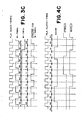
- Figs. 3A, 3B, and 3C are a state diagram, state table and state equation, and timing diagram that explain the generation of CTRENB by PLA 50 in response to the clock signal W.
- PLA 50 includes internal D type flip-flops that read the clock signal W on the low-to-high transistion of the 10 megahertz PLA clock.
- internal PLA signals So, S 1 that generate CTRENB are in state 00 awaiting the arrival of an input clock signal W from the multiplexer 61. W will be at its highest frequency, 5 megahertz.
- signals So, S 1 move to state 01 and CTRENB is thereby asserted (here active low) to cause PLAs 42, 44, 46 to count.
- CTRENB is ORed at gates 52, 54 with the carry signal CEOUT1 and CEOUT2, respectively, (also active low) from the preceding PLAs.
- the clock W signal has a frequency selected from one of the seven slower frequencies available, initially the 5 megahertz frequency.
- the W signal therefore persists after CTRENB disappears, as indicated in Figs. 3A, 3C, moving So, S 1 to state 11. So, S 1 remain in that state until W disappears, at which time they return to state 00.
- Signals So, S 1 return directly to state 00 from state 01; however, when W is a 5 megahertz signal, CTRENB is not again asserted until a new W clock signal then arrives.
- Figs. 4A, 4B, and 4C are a state diagram, state table and state equations, and timing diagram that explain the generation of INVCLR and CTRCLR by PLA 50 in response to the event signal and the mode signal.
- internal signals Sz, S 3 that generate CTRCLR and INVCLR are reset to state 00.
- CTRCLR is asserted to reset the counter PLAs to zero.
- S 2 , S 3 move from state 00 to state 10 but continue to assert CTRCLR through this PLA clock cycle. The event persists beyond the 10 megahertz PLA clock cycle as shown in Fig. 4C and S 2 , S 3 move to state 11, CTRCLR still being asserted.
- S 2 , S 3 remain in state 11 until the event signal disappears at the input of PLA 50. Once the event signal disappears, S 2 , S 3 return to state 10, CTRCLR still being asserted. S 2 , S 3 then move to state 01 and CTRCLR disappears, allowing the counter PLAs to count until another event occurs. From there S 2 , S 3 move to state 11, to state 10 and back to 01 until data acquisition is halted or a reset occurs.
- INVCLR is asserted once S z , S 3 are in state 11, one PLA 10 megahertz clock cycle after CTRCLR is asserted in transition from state 10 to 11 or 01 to 11. This delay provides the counter PLAs with time to clear and begin counting.
- the INVCLR signal clears flip-flop 64 and thereby changes the logic state of the INVCNT signal to memory 34. INVCLR remains asserted until S 2 , S 3 move to state 10 after the event signal disappears.
- Figs. 2 and 5 illustrate the configuring of a PLA 42, 44, and 46 to enable each to generate the Gray code count.
- the logic equations that show how each counter PLA counts are given below, where DIS, the enable input to the PLA, is active low: CEOUT1 is the external carry from PLA 42 to OR gate 54.
- CEOUT2 is the external carry from PLA 44 to OR gate 52.
- Figs. 6 and 7 illustrate the count generation of PLA 42, which is the same for PLAs 44 and 46 except for designation of the carry signals.
- PLA 42 initially generates a count of 0000 in a 3-bit counter, the three lower bits being the counter output and the upper bit being a status bit.
- CTRENB Each time CTRENB is asserted, the PLA moves to another state.
- the PLA On transition from state 0100 to 1100, the PLA asserts CEOUTA (an internal carry) simultaneously with the assertion of CTRENB.
- CEOUTA and CTRENB cause the internal 2-bit counter (again with a status bit) shown in Fig. 7 to move from one state to another, such as from state 000 to 001. Note that the three counter output bits of the 3-bit counter do not change during this transition.
- CEOUTA is again asserted in the state change of the 3-bit counter from 1000 to 0000. This process continues until the 2-bit counter generates CEOUT1 (the external carry to PLA 44) during the transition of the 2-bit counter from state 010 to 110 and from 100 to 000. During these two transitions, none of the output bits of the 2-bit counter or the 3- bit counter change, the transition occurring instead in a following counter PLA. For example, CEOUT1 is ORed with CTRENB to cause PLA 44 to count according to logic equation (2). This process continues with PLAs 44 and 46 as shown in logic equation (3) to generate the entire 15-bit Gray code count.
- the frequency at which W is generated is determined by the count of the upper three bits of the Gray code count produced by PLA 46, which are routed to the select lines of multiplexer 61. As these bits change, the slower frequencies are selected, thereby extending the time range of the circuit 12.
- PLA 46 also generates an overflow bit if the count reaches its maximum.
- circuit 12 could be implemented with conventional counters rather than PLAs, with other configurations of PLAs, or be produced as an integrated circuit. I therefore claim all modifications coming within the spirit and scope of the following claims.
Landscapes
- Engineering & Computer Science (AREA)
- General Engineering & Computer Science (AREA)
- Theoretical Computer Science (AREA)
- Computer Hardware Design (AREA)
- Quality & Reliability (AREA)
- Physics & Mathematics (AREA)
- General Physics & Mathematics (AREA)
- Measurement Of Unknown Time Intervals (AREA)
- Electromechanical Clocks (AREA)
- Electric Clocks (AREA)
Applications Claiming Priority (2)
| Application Number | Priority Date | Filing Date | Title |
|---|---|---|---|
| US06/906,873 US4731768A (en) | 1986-09-15 | 1986-09-15 | Autoranging time stamp circuit |
| US906873 | 1986-09-15 |
Publications (2)
| Publication Number | Publication Date |
|---|---|
| EP0260502A2 true EP0260502A2 (de) | 1988-03-23 |
| EP0260502A3 EP0260502A3 (de) | 1990-03-21 |
Family
ID=25423123
Family Applications (1)
| Application Number | Title | Priority Date | Filing Date |
|---|---|---|---|
| EP87112563A Withdrawn EP0260502A3 (de) | 1986-09-15 | 1987-08-28 | Zeitstempelschaltung mit automatischer Bereichregelung |
Country Status (3)
| Country | Link |
|---|---|
| US (1) | US4731768A (de) |
| EP (1) | EP0260502A3 (de) |
| JP (1) | JPS6371662A (de) |
Cited By (6)
| Publication number | Priority date | Publication date | Assignee | Title |
|---|---|---|---|---|
| EP0476250A1 (de) * | 1990-08-31 | 1992-03-25 | International Business Machines Corporation | Gerät zur Überwachung von Datenübertragungen in einer OEM-Kanalschnittstelle |
| EP0434081A3 (en) * | 1989-12-22 | 1992-04-15 | Bull Hn Information Systems Inc. | Monitor apparatus for selectively detecting signal conditions at points in an operating system |
| EP0547292A1 (de) * | 1991-12-19 | 1993-06-23 | Hewlett-Packard Company | Zeitmesser für Ereignisse im Picosekundenbereich |
| US6434211B1 (en) | 1997-10-16 | 2002-08-13 | The Victoria University Of Manchester | Timing circuit |
| FR2882834A1 (fr) * | 2005-03-04 | 2006-09-08 | Marc Hermelin | Systeme d'enregistrement d'evenements |
| CN108829620A (zh) * | 2018-05-28 | 2018-11-16 | 北京航空航天大学 | 一种异常小数据采集方法 |
Families Citing this family (13)
| Publication number | Priority date | Publication date | Assignee | Title |
|---|---|---|---|---|
| US5067130A (en) * | 1989-09-29 | 1991-11-19 | Tektronix, Inc. | Method for acquiring data in a logic analyzer |
| US5229981A (en) * | 1992-04-20 | 1993-07-20 | Maschi Louis P | Digital multi event timer |
| GB9304622D0 (en) * | 1993-03-06 | 1993-04-21 | Ncr Int Inc | Wireless local area network apparatus |
| US5446650A (en) * | 1993-10-12 | 1995-08-29 | Tektronix, Inc. | Logic signal extraction |
| US5526286A (en) * | 1994-02-16 | 1996-06-11 | Tektronix, Inc. | Oversampled logic analyzer |
| US5877621A (en) * | 1996-04-30 | 1999-03-02 | Hewlett-Packard Company | Digital oscilloscope with pan and zoom produced from time stamped data records indexed by trigger offset |
| US6742059B1 (en) * | 2000-02-04 | 2004-05-25 | Emc Corporation | Primary and secondary management commands for a peripheral connected to multiple agents |
| US6542838B1 (en) * | 2000-05-12 | 2003-04-01 | National Instruments Corporation | System and method for performing autoranging in a measurement device |
| US7113886B2 (en) * | 2002-01-23 | 2006-09-26 | Credence Systems Corporation | Circuit and method for distributing events in an event stream |
| US6950375B2 (en) * | 2002-12-17 | 2005-09-27 | Agilent Technologies, Inc. | Multi-phase clock time stamping |
| US8295182B2 (en) * | 2007-07-03 | 2012-10-23 | Credence Systems Corporation | Routed event test system and method |
| US8050148B2 (en) * | 2008-07-03 | 2011-11-01 | Texas Instruments Incorporated | Flash time stamp apparatus |
| JP5308133B2 (ja) * | 2008-11-27 | 2013-10-09 | インターナショナル・ビジネス・マシーンズ・コーポレーション | 測定データの転送制御装置及び方法 |
Family Cites Families (6)
| Publication number | Priority date | Publication date | Assignee | Title |
|---|---|---|---|---|
| US4031739A (en) * | 1976-07-22 | 1977-06-28 | Springer Barry R | Autoranging method and system for testing the speeds of a camera shutter |
| US4107600A (en) * | 1976-12-13 | 1978-08-15 | General Electric Company | Adaptive frequency to digital converter system |
| DE3132984A1 (de) * | 1981-08-20 | 1983-03-10 | Siemens AG, 1000 Berlin und 8000 München | Logikanalysator |
| EP0094976B1 (de) * | 1982-05-24 | 1986-08-27 | Ibm Deutschland Gmbh | Logik-Analysator |
| US4590602A (en) * | 1983-08-18 | 1986-05-20 | General Signal | Wide range clock recovery circuit |
| US4546487A (en) * | 1983-12-30 | 1985-10-08 | Rca Corporation | Auto ranging counter |
-
1986
- 1986-09-15 US US06/906,873 patent/US4731768A/en not_active Expired - Lifetime
-
1987
- 1987-08-28 EP EP87112563A patent/EP0260502A3/de not_active Withdrawn
- 1987-09-09 JP JP62226233A patent/JPS6371662A/ja active Pending
Cited By (8)
| Publication number | Priority date | Publication date | Assignee | Title |
|---|---|---|---|---|
| EP0434081A3 (en) * | 1989-12-22 | 1992-04-15 | Bull Hn Information Systems Inc. | Monitor apparatus for selectively detecting signal conditions at points in an operating system |
| EP0476250A1 (de) * | 1990-08-31 | 1992-03-25 | International Business Machines Corporation | Gerät zur Überwachung von Datenübertragungen in einer OEM-Kanalschnittstelle |
| US5297277A (en) * | 1990-08-31 | 1994-03-22 | International Business Machines Corporation | Apparatus for monitoring data transfers of an oemi channel interface |
| EP0547292A1 (de) * | 1991-12-19 | 1993-06-23 | Hewlett-Packard Company | Zeitmesser für Ereignisse im Picosekundenbereich |
| US6434211B1 (en) | 1997-10-16 | 2002-08-13 | The Victoria University Of Manchester | Timing circuit |
| FR2882834A1 (fr) * | 2005-03-04 | 2006-09-08 | Marc Hermelin | Systeme d'enregistrement d'evenements |
| CN108829620A (zh) * | 2018-05-28 | 2018-11-16 | 北京航空航天大学 | 一种异常小数据采集方法 |
| CN108829620B (zh) * | 2018-05-28 | 2019-05-17 | 北京航空航天大学 | 一种异常小数据采集方法 |
Also Published As
| Publication number | Publication date |
|---|---|
| EP0260502A3 (de) | 1990-03-21 |
| US4731768A (en) | 1988-03-15 |
| JPS6371662A (ja) | 1988-04-01 |
Similar Documents
| Publication | Publication Date | Title |
|---|---|---|
| US4731768A (en) | Autoranging time stamp circuit | |
| US4924468A (en) | Logic analyzer | |
| US4425643A (en) | Multi-speed logic analyzer | |
| KR100197745B1 (ko) | Ic반도체칩 연산속도 테스트용의 전자회로 및 그 방법 | |
| US6275782B1 (en) | Non-intrusive performance monitoring | |
| US4257108A (en) | Pulse generator | |
| JP2819007B2 (ja) | ロジックアナライザ | |
| US5136180A (en) | Variable frequency clock for a computer system | |
| US4726045A (en) | Low jitter digital delay generator | |
| US4752928A (en) | Transaction analyzer | |
| US6081484A (en) | Measuring signals in a tester system | |
| US4558422A (en) | Digital signal sampling system with two unrelated sampling timebases | |
| CA1194550A (en) | Circuit for detecting signal generation sequence | |
| EP0425080A2 (de) | Verfahren und digitales Datenerfassungsinstrument mit Zähler/Zeitgeber zum Markieren von Zeitintervallen, insbesondere in einem Logikanalysator | |
| US4737792A (en) | Counter-based simulated target generator | |
| US6215345B1 (en) | Semiconductor device for setting delay time | |
| US11178036B2 (en) | Systems and methods for measuring latency in a network device | |
| US3843893A (en) | Logical synchronization of test instruments | |
| US4208626A (en) | Precision timing source for multiple rate sampling of high-speed waveforms | |
| US7197419B2 (en) | System and method for thermal monitoring of IC using sampling periods of invariant duration | |
| EP0120452B1 (de) | Verfahren zum Datenvergleich mit asynchronen Zeitbasen | |
| WO1987001207A1 (en) | Harmonic sampling logic analyzer | |
| JP3206010B2 (ja) | タイムスタンプ回路 | |
| US5483648A (en) | Circuit for determining the arrival times of control signals supplied to microprocessors | |
| KR940009815B1 (ko) | 마이컴의 직렬포트를 이용한 주파수 측정장치 및 방법 |
Legal Events
| Date | Code | Title | Description |
|---|---|---|---|
| PUAI | Public reference made under article 153(3) epc to a published international application that has entered the european phase |
Free format text: ORIGINAL CODE: 0009012 |
|
| AK | Designated contracting states |
Kind code of ref document: A2 Designated state(s): DE FR GB NL |
|
| PUAL | Search report despatched |
Free format text: ORIGINAL CODE: 0009013 |
|
| AK | Designated contracting states |
Kind code of ref document: A3 Designated state(s): DE FR GB NL |
|
| STAA | Information on the status of an ep patent application or granted ep patent |
Free format text: STATUS: THE APPLICATION IS DEEMED TO BE WITHDRAWN |
|
| 18D | Application deemed to be withdrawn |
Effective date: 19900924 |
|
| RIN1 | Information on inventor provided before grant (corrected) |
Inventor name: EASTERDAY, JOHN L. |