EP0261366A1 - Amplificateur de puissance numérique rapide - Google Patents
Amplificateur de puissance numérique rapide Download PDFInfo
- Publication number
- EP0261366A1 EP0261366A1 EP87111421A EP87111421A EP0261366A1 EP 0261366 A1 EP0261366 A1 EP 0261366A1 EP 87111421 A EP87111421 A EP 87111421A EP 87111421 A EP87111421 A EP 87111421A EP 0261366 A1 EP0261366 A1 EP 0261366A1
- Authority
- EP
- European Patent Office
- Prior art keywords
- semiconductor switches
- switched
- power amplifier
- partial voltage
- digital power
- Prior art date
- Legal status (The legal status is an assumption and is not a legal conclusion. Google has not performed a legal analysis and makes no representation as to the accuracy of the status listed.)
- Withdrawn
Links
- 239000004065 semiconductor Substances 0.000 claims abstract description 31
- 230000002452 interceptive effect Effects 0.000 abstract 1
- 230000005669 field effect Effects 0.000 description 2
- 230000005540 biological transmission Effects 0.000 description 1
- 238000011161 development Methods 0.000 description 1
- 230000018109 developmental process Effects 0.000 description 1
- 238000010586 diagram Methods 0.000 description 1
- 238000009826 distribution Methods 0.000 description 1
- 238000004519 manufacturing process Methods 0.000 description 1
- 230000003595 spectral effect Effects 0.000 description 1
- 230000002123 temporal effect Effects 0.000 description 1
- 238000009827 uniform distribution Methods 0.000 description 1
Images

Classifications
-
- H—ELECTRICITY
- H03—ELECTRONIC CIRCUITRY
- H03K—PULSE TECHNIQUE
- H03K17/00—Electronic switching or gating, i.e. not by contact-making and –breaking
- H03K17/08—Modifications for protecting switching circuit against overcurrent or overvoltage
- H03K17/081—Modifications for protecting switching circuit against overcurrent or overvoltage without feedback from the output circuit to the control circuit
- H03K17/0814—Modifications for protecting switching circuit against overcurrent or overvoltage without feedback from the output circuit to the control circuit by measures taken in the output circuit
- H03K17/08142—Modifications for protecting switching circuit against overcurrent or overvoltage without feedback from the output circuit to the control circuit by measures taken in the output circuit in field-effect transistor switches
-
- H—ELECTRICITY
- H03—ELECTRONIC CIRCUITRY
- H03F—AMPLIFIERS
- H03F3/00—Amplifiers with only discharge tubes or only semiconductor devices as amplifying elements
- H03F3/20—Power amplifiers, e.g. Class B amplifiers, Class C amplifiers
- H03F3/21—Power amplifiers, e.g. Class B amplifiers, Class C amplifiers with semiconductor devices only
- H03F3/217—Class D power amplifiers; Switching amplifiers
- H03F3/2175—Class D power amplifiers; Switching amplifiers using analogue-digital or digital-analogue conversion
-
- H—ELECTRICITY
- H03—ELECTRONIC CIRCUITRY
- H03K—PULSE TECHNIQUE
- H03K17/00—Electronic switching or gating, i.e. not by contact-making and –breaking
- H03K17/10—Modifications for increasing the maximum permissible switched voltage
- H03K17/102—Modifications for increasing the maximum permissible switched voltage in field-effect transistor switches
Definitions
- the invention relates to a fast digital power amplifier according to the preamble of patent claim 1.
- Such a power amplifier can be used, for example, as a modulation amplifier in an amplitude-modulated (AM) radio transmitter.
- AM amplitude-modulated
- Modulation amplifiers that can amplify direct and low-frequency alternating voltage (LF voltage) are suitable as modulation amplifiers for AM radio transmitters.
- An advantageous circuit of a digital amplifier consists in a series connection of individual, separately controllable voltage sources with binary weighting, as described in German Offenlegungsschrift DE 30 44 956 A1 is known.
- a high switching frequency is required and a low-pass filter downstream of the series connection of voltage sources is required to eliminate unwanted spectral components at the output of the amplifier.
- the amplifier specified in DE 30 44 956 A1 has the disadvantage that it is unsuitable as a power amplifier for the stated purpose, since the switching on and off of the semiconductor switches of the individual voltage sources cannot be carried out with a high switching frequency specified by the quality requirements for radio transmitters .
- the low-frequency transmission bandwidth is currently generally around 5 kHz.
- the modulation amplifier must be followed by a low-pass filter, the cutoff frequency of which is above the highest low frequency to be transmitted and below the switching frequency.
- the invention has for its object to improve a generic switching amplifier in such a way that the (partial) voltage sources can be switched on the one hand with a high switching frequency and on the other hand the associated switches avoid exceeding a specifiable electrical power loss.
- An advantage of the invention is that, despite an advantageously high switching frequency with which the partial voltage sources are operated, the associated semiconductor switches can be controlled with such a low switching frequency that an electrical power loss occurring in the semiconductor switches does not exceed certain permissible values.
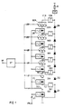
- Each partial voltage source is d from the supply network VN, z. B. 220 V, 50 Hz, fed via a two-wire line and contains a rectifier arrangement.
- These partial DC voltages can be added via a diode cascade D1 to DN, so that a maximum DC voltage is present at the amplifier output of 630 V, in minimum steps of 10 V, can be generated.
- the connecting lines VL1 to VLN between the partial voltage sources U1 to UN and the associated diodes of the diode cascade D1 to DN each contain a peak current limiter SB1 to SBN, which essentially limits disturbing commutation current peaks that arise to a non-disturbing maximum current.
- the switch arrangement specified is a controllable half-turn circuit.
- power transistors, field-effect transistors, thyristors or GTOs are suitable as semiconductors.
- the partial voltage source U1 selected as an example has an associated freewheeling diode D1, via which the current of the switching amplifier flows in the case of the blocked semiconductor switch. When all partial voltage sources U1 to UN are switched off, no more current flows.
- NG1 denotes a preferably three-phase rectifier.
- the peak current limiters SB1 to SBN limit the current peak which is essentially caused by the commutation current of the freewheeling diode when the switch arrangements are switched on, as a result of which significantly higher operating currents for the partial voltage sources U1 to UN are possible.
- Such a device is particularly advantageous in the case of partial voltage sources which use field-effect transistors as the switch arrangement.
- the peak current limiter SB1 consists in the simplest case of an ohmic resistor.
- Another exemplary embodiment of a peak current limiter is a parallel connection of the resistor and the coil (FIG. 3), it being possible as an alternative to provide a diode in one or both parallel circuits in series with the resistor and the coil (FIG. 4).
- the current limiter is arranged between the output of the switch arrangement and the output of the free-wheeling diode.
- the rectifier arrangement is connected in series with a switch group BG1 to BGN, so that the DC voltage generated in each case can be switched.
- At least one of the switch groups BG1 to BGN is formed by separately controllable, parallel-connected semiconductor switches.
- the number of semiconductor switches to be connected in parallel is determined from the ratio of the switching frequency of a switch group to the maximum permissible switching frequency of the semiconductor switches.
- the number of semiconductor switches connected in parallel in the individual switch groups can be different. For example, B. in all Groups with smaller binary voltage values, because of the lower switching losses and the availability of faster semiconductor switches for lower voltages, fewer semiconductor switches are connected in parallel than with the switch groups with high voltage values.
- the control of the individual semiconductor switches in the various switch groups is carried out by a control unit ST, at the input of which the LF signal or a corresponding signal is present and from whose output multi-core control lines lead to the switch groups.
- a time-uniform distribution of the power loss of the semiconductor switches is achieved in that the semiconductor switches connected in parallel are switched on and off in sequence and the semiconductor switches of the switch groups which have not been used for the longest time are first switched on again. This not only achieves an optimal temporal distribution of the switching losses on the individual semiconductor switches, but at the same time avoids the immediate reclosure of a semiconductor switch that has just been switched off, which is disadvantageous for semiconductor switches in circuit arrangements with free-wheeling diodes because of their high commutation currents.
Landscapes
- Engineering & Computer Science (AREA)
- Power Engineering (AREA)
- Electronic Switches (AREA)
- Amplifiers (AREA)
Applications Claiming Priority (2)
| Application Number | Priority Date | Filing Date | Title |
|---|---|---|---|
| DE3632716 | 1986-09-26 | ||
| DE19863632716 DE3632716A1 (de) | 1986-09-26 | 1986-09-26 | Schneller digitaler leistungsverstaerker |
Publications (1)
| Publication Number | Publication Date |
|---|---|
| EP0261366A1 true EP0261366A1 (fr) | 1988-03-30 |
Family
ID=6310403
Family Applications (1)
| Application Number | Title | Priority Date | Filing Date |
|---|---|---|---|
| EP87111421A Withdrawn EP0261366A1 (fr) | 1986-09-26 | 1987-08-07 | Amplificateur de puissance numérique rapide |
Country Status (2)
| Country | Link |
|---|---|
| EP (1) | EP0261366A1 (fr) |
| DE (1) | DE3632716A1 (fr) |
Cited By (2)
| Publication number | Priority date | Publication date | Assignee | Title |
|---|---|---|---|---|
| EP0349732A1 (fr) * | 1988-07-07 | 1990-01-10 | TELEFUNKEN Sendertechnik GmbH | Amplificateur de puissance |
| EP0549101A3 (en) * | 1991-11-20 | 1993-09-22 | Continental Electronics Corporation | Amplifier with multiple switched stages and noise suppression |
Families Citing this family (1)
| Publication number | Priority date | Publication date | Assignee | Title |
|---|---|---|---|---|
| DE4135259C1 (fr) * | 1991-10-25 | 1993-01-07 | Semikron Elektronik Gmbh, 8500 Nuernberg, De |
Citations (4)
| Publication number | Priority date | Publication date | Assignee | Title |
|---|---|---|---|---|
| EP0058443A1 (fr) * | 1981-02-16 | 1982-08-25 | BBC Brown Boveri AG | Procédé pour amplifier un signal analogique à basse fréquence au moyen d'un amplificateur à commutation et amplificateur à commutation pour la mise en oeuvre du dit procédé |
| EP0083727A1 (fr) * | 1981-12-24 | 1983-07-20 | Harris Corporation | Modulateur d'amplitude |
| EP0124765A1 (fr) * | 1983-05-10 | 1984-11-14 | BBC Brown Boveri AG | Amplificateur de puissance à commutation numérique |
| EP0218152A1 (fr) * | 1985-09-28 | 1987-04-15 | Licentia Patent-Verwaltungs-GmbH | Amplificateur à commutation |
-
1986
- 1986-09-26 DE DE19863632716 patent/DE3632716A1/de not_active Withdrawn
-
1987
- 1987-08-07 EP EP87111421A patent/EP0261366A1/fr not_active Withdrawn
Patent Citations (4)
| Publication number | Priority date | Publication date | Assignee | Title |
|---|---|---|---|---|
| EP0058443A1 (fr) * | 1981-02-16 | 1982-08-25 | BBC Brown Boveri AG | Procédé pour amplifier un signal analogique à basse fréquence au moyen d'un amplificateur à commutation et amplificateur à commutation pour la mise en oeuvre du dit procédé |
| EP0083727A1 (fr) * | 1981-12-24 | 1983-07-20 | Harris Corporation | Modulateur d'amplitude |
| EP0124765A1 (fr) * | 1983-05-10 | 1984-11-14 | BBC Brown Boveri AG | Amplificateur de puissance à commutation numérique |
| EP0218152A1 (fr) * | 1985-09-28 | 1987-04-15 | Licentia Patent-Verwaltungs-GmbH | Amplificateur à commutation |
Cited By (3)
| Publication number | Priority date | Publication date | Assignee | Title |
|---|---|---|---|---|
| EP0349732A1 (fr) * | 1988-07-07 | 1990-01-10 | TELEFUNKEN Sendertechnik GmbH | Amplificateur de puissance |
| DE3822990A1 (de) * | 1988-07-07 | 1990-01-11 | Olympia Aeg | Leistungsverstaerker |
| EP0549101A3 (en) * | 1991-11-20 | 1993-09-22 | Continental Electronics Corporation | Amplifier with multiple switched stages and noise suppression |
Also Published As
| Publication number | Publication date |
|---|---|
| DE3632716A1 (de) | 1988-03-31 |
Similar Documents
| Publication | Publication Date | Title |
|---|---|---|
| DE3044956C2 (de) | Verstärker | |
| DE69330355T2 (de) | Verstärkerausgangsstufe | |
| EP0025234B1 (fr) | Amplificateur de puissance basse fréquence et application à un émetteur à modulation d'amplitude | |
| EP0218152B1 (fr) | Amplificateur à commutation | |
| DE3534678A1 (de) | Schaltverstaerker | |
| DE69408115T2 (de) | Verstärker mit hohem Wirkungsgrad mit verminderter Schaltungsverzerrung | |
| EP0261366A1 (fr) | Amplificateur de puissance numérique rapide | |
| DE2854441A1 (de) | Gleichspannungsregler | |
| DE3215589A1 (de) | Beschaltung ohne prinzipbedingte verluste fuer elektronische zweigpaare in antiparallelschaltung | |
| DE2904231A1 (de) | Elektrischer verstaerker | |
| EP0267391B1 (fr) | Amplificateur à commutation | |
| DE1277356B (de) | Gleichstrom-Fernversorgung von Fernsprechverstaerkern | |
| EP0048490B1 (fr) | Circuit pour transformer un signal d'entrée binaire en un signal télégraphique | |
| DE3321999C2 (fr) | ||
| DE2952654A1 (de) | Gegentakt-wechselrichter | |
| DE4042378C2 (fr) | ||
| DE2814706C3 (de) | Sperrwandleranordnung | |
| DE929619C (de) | Transistor-Vermittlungsnetzwerk mit Nummerngruppenkreis fuer Nachrichtensysteme | |
| DE1245429B (de) | Verstaerkerschaltung mit zwei Transistoren, deren Emitter-Kollektor-Strecken in Reihe an die Speisespannung angeschlossen sind | |
| DE60118847T2 (de) | Schaltung zur signalverarbeitung mit einer klasse a/b- ausgangsstufe zum anschluss an eine quelle für eine vielzahl von versorgungsspannungen | |
| DE2043284C3 (de) | Kodierungsübersetzerschaltung zur Anwendung in einem beigeordneten Gedächtnissystem | |
| DE3430308A1 (de) | Stromrichter | |
| DE2056073A1 (de) | Rundfunkempfangsgerät mit einem Umschalter | |
| DE1763778C3 (de) | Elektronisches Mehrfach-Fernsteuenuigssystem | |
| EP0905872B1 (fr) | Alimentation commandable de courant continu à haute tension et son emploi |
Legal Events
| Date | Code | Title | Description |
|---|---|---|---|
| PUAI | Public reference made under article 153(3) epc to a published international application that has entered the european phase |
Free format text: ORIGINAL CODE: 0009012 |
|
| AK | Designated contracting states |
Kind code of ref document: A1 Designated state(s): CH DE FR GB LI |
|
| 17P | Request for examination filed |
Effective date: 19880915 |
|
| STAA | Information on the status of an ep patent application or granted ep patent |
Free format text: STATUS: THE APPLICATION IS DEEMED TO BE WITHDRAWN |
|
| 18D | Application deemed to be withdrawn |
Effective date: 19910301 |
|
| RIN1 | Information on inventor provided before grant (corrected) |
Inventor name: LODAHL, MANFRED, DIPL.-ING. |