EP0261620A2 - Montage et circuit de bus à largeur de bande élevée ainsi qu'un composant de réseau de connexion à large bande - Google Patents
Montage et circuit de bus à largeur de bande élevée ainsi qu'un composant de réseau de connexion à large bande Download PDFInfo
- Publication number
- EP0261620A2 EP0261620A2 EP87113757A EP87113757A EP0261620A2 EP 0261620 A2 EP0261620 A2 EP 0261620A2 EP 87113757 A EP87113757 A EP 87113757A EP 87113757 A EP87113757 A EP 87113757A EP 0261620 A2 EP0261620 A2 EP 0261620A2
- Authority
- EP
- European Patent Office
- Prior art keywords
- signal
- bandwidth
- circuit arrangement
- circuit
- arrangement according
- Prior art date
- Legal status (The legal status is an assumption and is not a legal conclusion. Google has not performed a legal analysis and makes no representation as to the accuracy of the status listed.)
- Ceased
Links
Images


Classifications
-
- H—ELECTRICITY
- H04—ELECTRIC COMMUNICATION TECHNIQUE
- H04L—TRANSMISSION OF DIGITAL INFORMATION, e.g. TELEGRAPHIC COMMUNICATION
- H04L12/00—Data switching networks
- H04L12/28—Data switching networks characterised by path configuration, e.g. LAN [Local Area Networks] or WAN [Wide Area Networks]
- H04L12/40—Bus networks
- H04L12/4013—Management of data rate on the bus
-
- H—ELECTRICITY
- H04—ELECTRIC COMMUNICATION TECHNIQUE
- H04B—TRANSMISSION
- H04B3/00—Line transmission systems
-
- H—ELECTRICITY
- H04—ELECTRIC COMMUNICATION TECHNIQUE
- H04Q—SELECTING
- H04Q3/00—Selecting arrangements
- H04Q3/42—Circuit arrangements for indirect selecting controlled by common circuits, e.g. register controller, marker
- H04Q3/52—Circuit arrangements for indirect selecting controlled by common circuits, e.g. register controller, marker using static devices in switching stages, e.g. electronic switching arrangements
- H04Q3/521—Circuit arrangements for indirect selecting controlled by common circuits, e.g. register controller, marker using static devices in switching stages, e.g. electronic switching arrangements using semiconductors in the switching stages
Definitions
- the invention relates to a circuit arrangement according to the preamble of claim 1, a bus circuit according to the preamble of claim 7 and a broadband switching matrix device according to the preamble of claim 8.
- a broadband switching matrix module in which a connection between one of several signal inputs and one of several signal outputs can be established by a plurality of coupling points, has such a bus circuit for each signal output, with one driver circuit being available for each signal input and bus circuit.
- the bandwidth of such a broadband switching module depends directly on the number of signal inputs. For a given technology and for a given bandwidth, the size of the switching matrix is also given, provided that no measures can be taken to increase the bandwidth in the given technology.
- the invention is remedied by a circuit arrangement according to the teaching of claim 1, a bus circuit according to the teaching of claim 7 and a broadband switching matrix module according to the teaching of claim 8.
- the fixed potential is advantageously chosen in the middle of the supply voltage, in the case of analog circuits at the operating point. If a second resistor is added, which is connected to a second point with a different potential, there is a voltage divider with which both the effective resistance and a potential that does not influence the function of the circuit can be set. In the case of integrated circuit technology in particular, the resistors are advantageously implemented by transistors.
- the circuit measure according to the invention naturally has not only advantageous effects.
- the signal swing is reduced because the product of gain and bandwidth is constant.
- the use of transistors has the advantage that they can be switched off when this part of the circuit is not required and that the control can be adapted to the bandwidth actually required by changing the control. Because of the reduction in the signal swing and the associated additional interference possibilities, such a measure should only be taken where it is absolutely necessary, ie between those two stages in the course of a signal path between which the bandwidth is most limited.
- a broadband switching matrix module in which a signal between a signal input and a signal output passes through a series of signal conditioning and monitoring circuits, e.g. input and output isolating amplifiers and synchronization circuits, in addition to the actual switching matrix, the greatest band limitation occurs in the switching matrix, as already described the bus circuits that lead to a common signal output.
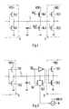
- a transmitting part S is connected to a receiving part E via a signal line L.
- Transmitting part S and receiving part E are any two successive stages in the course of a signal path.
- the transmitting part S is characterized by an internal resistance Ri and an original voltage source uo.
- the original voltage source uo is shown in the drawing as the source of a digital signal.
- the receiving part E is characterized by an input resistance Re. It is assumed that the signal line L is so short that it does not have to be terminated with its characteristic impedance. In such cases, the input resistance Re is orders of magnitude larger than the internal resistance Ri.
- the output of the transmitting part S, the input of the receiving part E and the signal line L have inevitable capacitances, which is shown in FIG. 1 as capacitance C going to ground are drawn. It is evident that the internal resistance Ri and the capacitance C form a low pass.
- the input resistance Re is connected in parallel with the internal resistance Ri in terms of alternating current and does not fundamentally change the low-pass characteristic.
- a further resistance Ra is now connected in parallel with the internal resistance Ri in terms of alternating current. Basically, this does not change the low-pass behavior; however, the upper limit frequency and thus the bandwidth can be increased significantly.
- This basic circuit also shows that the signal swing is reduced by this measure.
- auxiliary voltage source UH is inserted between the resistor Ra and ground in FIG.
- This auxiliary voltage source UH which is a DC voltage source, has no influence on the frequency response of the circuit arrangement.
- Resistor Ra can be connected to any point of fixed potential.
- the ground and supply voltage potentials that are present anyway come into question.
- the fixed potential can also be in the middle of the supply voltage. This is particularly important when the circuit arrangement is non-linear.
- FIG. 2 shows a practical embodiment of the basic circuit of FIG. 1.
- the transmitting part contains a driver circuit consisting of two transistors TS1 and TS2, which is between the supply voltage VDD and ground. Both transistors TS1 and TS2 are driven together, one of the two being conductive and the other blocking.
- the receiving part S contains, likewise between the supply voltage VDD and ground, a similar input circuit consisting of two transistors TE1 and TE2, which are controlled by the output signal of the transmitting part S via the signal line L.
- the resistor Ra is connected to half the supply voltage VDD / 2.
- FIG. 3 shows a slight modification of the example according to FIG. 2.
- the resistor Ra is divided into two resistors R1 and R2, one of which is connected to ground, the other to the supply voltage VDD.
- the auxiliary voltage can thus be influenced via the ratio of the resistors R1 and R2 and the bandwidth can be influenced via the absolute value of the two resistors.
- FIG. 4 shows a modification of the circuit according to FIG. 3 for the practically very significant case in which the circuit arrangement is part of an integrated circuit.
- the resistors R1 and R2 are also designed as transistors, here Ta1 and Ta2.
- the control of the two transistors via a control Voltage Us1 and a control voltage Us2 are DC-voltage, can be both permanently connected and can be set as desired from the outside. This makes it possible to keep the reduction in the signal swing and the power loss in the transistors Ta1 and Ta2 as small as possible, depending on the respective application.
- FIG. 5 shows a further exemplary embodiment which combines features of the exemplary embodiment according to FIG. 2 and features of the exemplary embodiment according to FIG. 4.
- the resistor Ra in FIG. 2 is replaced here by a parallel connection of two transistors Ta1 and Ta2. These are driven in opposite directions by means of a control voltage Us with the aid of an inverter (not specified in more detail), so that they are both switched on or both switched off because of the opposite polarity.
- This circuit arrangement can only be used for a switchover that is sufficient for many practical cases.
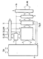
- FIG. 6 shows the block diagram of a broadband switching matrix module with 16 signal inputs E1 to E16, 16 extension inputs EX1 to EX16, a clock input TE, a clock output TA, 16 signal outputs A1 to A16 and a control data bus BUS.
- the signal paths reach the inside of the broadband switching matrix module via input isolating amplifier 3 and back out again via output isolating amplifier 4.
- the signals arriving via the signal inputs E1 to E16 are synchronized in an input synchronization device 1, and before leaving the broadband switching matrix module they are synchronized again in an output synchronization device 2.
- the expansion inputs EX1 to EX16 are connected to signal outputs A1 to A16 of a spatially immediately adjacent preceding switching matrix.
- the core of the broadband switching matrix is a switching matrix K.
- a monitoring device 5 is arranged at the output of the switching matrix K, which allows the 16 output signals to be monitored.
- a decoding and control device 6 is provided for controlling the coupling matrix K and for monitoring using the monitoring device 5. Further details on this switching matrix module, which, however, are not necessary for an understanding of the present invention, are contained in the following German patent applications: P 34 41 501.7, P 35 04 835.2, P 35 10 566.6 and P 35 43 392.2.
- the coupling matrix K is made up of rows and columns, each row being assigned to one of the signal outputs A1 to A16 and each column to one of the signal inputs E1 to E16 or one of the extension inputs EX1 to EX16.
- a coupling point K0101 to K1616 is arranged at the intersection of a column, which is assigned to one of the signal inputs E1 to E16, with a row.
- Each coupling point has two pairs of transistors, one pair of transistors being driven by a control signal St and the second pair of transistors by the signal coming from the assigned signal input.
- the control signal is inverted at each crosspoint, so that either both transistors of the associated transistor pair are open or both are closed.
- the control signal St comes from the decoding and control device 6.
- Each coupling point forms a driver circuit, at most one driver circuit is active, while all others are blocked and represent a capacitive load for the active driver circuit.
- a large number of further signal inputs can be indirectly connected to this bus circuit via the associated extension input, which can be connected to the associated signal output of a preceding broadband switching matrix device, without significantly burdening it.
- This is one way of increasing the number of signal inputs for a given bandwidth.
- the invention now provides a further possibility for increasing the number of signal inputs for a given bandwidth. This is equivalent to the possibility of increasing the bandwidth for a given number of signal inputs.
- an additional resistor is inserted. This is represented in FIG. 7 by the circuits designated as resistors R1 to R16.
- the control signals St can be used primarily to make this circuit high-impedance when the outputs are not connected. *
Landscapes
- Engineering & Computer Science (AREA)
- Computer Networks & Wireless Communication (AREA)
- Signal Processing (AREA)
- Quality & Reliability (AREA)
- Electronic Switches (AREA)
- Logic Circuits (AREA)
- Dc Digital Transmission (AREA)
- Cable Transmission Systems, Equalization Of Radio And Reduction Of Echo (AREA)
- Use Of Switch Circuits For Exchanges And Methods Of Control Of Multiplex Exchanges (AREA)
Applications Claiming Priority (2)
| Application Number | Priority Date | Filing Date | Title |
|---|---|---|---|
| DE3632218 | 1986-09-23 | ||
| DE19863632218 DE3632218A1 (de) | 1986-09-23 | 1986-09-23 | Schaltungsanordnung und busschaltung mit hoher bandbreite sowie breitbandkoppelfeldbaustein |
Publications (2)
| Publication Number | Publication Date |
|---|---|
| EP0261620A2 true EP0261620A2 (fr) | 1988-03-30 |
| EP0261620A3 EP0261620A3 (fr) | 1988-10-05 |
Family
ID=6310106
Family Applications (1)
| Application Number | Title | Priority Date | Filing Date |
|---|---|---|---|
| EP87113757A Ceased EP0261620A3 (fr) | 1986-09-23 | 1987-09-21 | Montage et circuit de bus à largeur de bande élevée ainsi qu'un composant de réseau de connexion à large bande |
Country Status (4)
| Country | Link |
|---|---|
| EP (1) | EP0261620A3 (fr) |
| JP (1) | JPS6387018A (fr) |
| AU (1) | AU593382B2 (fr) |
| DE (1) | DE3632218A1 (fr) |
Cited By (1)
| Publication number | Priority date | Publication date | Assignee | Title |
|---|---|---|---|---|
| EP0339719A1 (fr) * | 1988-04-25 | 1989-11-02 | AT&T NETWORK SYSTEMS INTERNATIONAL B.V. | Matrice de commutation pour centraux de télécommunication |
Family Cites Families (3)
| Publication number | Priority date | Publication date | Assignee | Title |
|---|---|---|---|---|
| JPS5362479A (en) * | 1976-11-16 | 1978-06-03 | Nec Corp | Integrated circuit with power terminals for testing |
| US4585958A (en) * | 1983-12-30 | 1986-04-29 | At&T Bell Laboratories | IC chip with noise suppression circuit |
| JPS60224356A (ja) * | 1984-04-23 | 1985-11-08 | Nec Corp | バス回路 |
-
1986
- 1986-09-23 DE DE19863632218 patent/DE3632218A1/de not_active Withdrawn
-
1987
- 1987-09-10 AU AU78255/87A patent/AU593382B2/en not_active Ceased
- 1987-09-21 EP EP87113757A patent/EP0261620A3/fr not_active Ceased
- 1987-09-22 JP JP62236386A patent/JPS6387018A/ja active Pending
Cited By (1)
| Publication number | Priority date | Publication date | Assignee | Title |
|---|---|---|---|---|
| EP0339719A1 (fr) * | 1988-04-25 | 1989-11-02 | AT&T NETWORK SYSTEMS INTERNATIONAL B.V. | Matrice de commutation pour centraux de télécommunication |
Also Published As
| Publication number | Publication date |
|---|---|
| EP0261620A3 (fr) | 1988-10-05 |
| AU7825587A (en) | 1988-03-31 |
| DE3632218A1 (de) | 1988-03-31 |
| JPS6387018A (ja) | 1988-04-18 |
| AU593382B2 (en) | 1990-02-08 |
Similar Documents
| Publication | Publication Date | Title |
|---|---|---|
| DE3215671C2 (de) | Programmierbare Logikanordnung | |
| DE2036306A1 (de) | Mehrfachverstärker, insbesondere in integrierter Schaltung, mit Stufenentkopplung | |
| EP0591561A1 (fr) | Circuit intégré pour générer un signal de remise à l'état initial | |
| DE2932587C2 (de) | Breitbandkoppelanordnung mit einer Matrix von Koppelpunktschaltkreisen in ECL-Technik | |
| EP0148395B1 (fr) | Champ de couplage à large bande sous forme de matrice | |
| DE3327488C2 (de) | Zweirichtungs-Verstärker für bidirektionale Datenleitungen | |
| DE4420988A1 (de) | Verfahren zum Testen einer integrierten Schaltung sowie integrierte Schaltungsanordnung mit einer Testschaltung | |
| EP0262480B1 (fr) | Circuit miroir de courant | |
| DE2251444C2 (de) | Koppelfeld-Anordnung zur breitbandigen Signalübertragung in Fernmeldeanlagen | |
| DE1268669B (de) | Multistabile Schaltung | |
| DE2208829A1 (fr) | ||
| EP0142182B1 (fr) | Montage pour la conversion d'un signal d'entrée numérique en un signal de sortie analogique | |
| DE1922382C3 (de) | Elektronische Koppelfeldeinrichtung mit Feldeffekttransistoren | |
| EP0261620A2 (fr) | Montage et circuit de bus à largeur de bande élevée ainsi qu'un composant de réseau de connexion à large bande | |
| EP0057239A1 (fr) | Circuit d'attaque du type push-pull monolithiquement intégré | |
| DE1541874A1 (de) | Daempfungs-Schaltung | |
| DE4231178C2 (de) | Speicherelement | |
| DE2002578C3 (de) | Multistabile Schaltung | |
| DE4421419A1 (de) | MOS-Treiberschaltung | |
| DE3032970C2 (de) | Schaltungsanordnung zur Symmetrierung der Arbeitspunkte bei elektronisch gleichstromgespeisten Anschlußleitungen in Fernmelde-, insbesondere Fernsprechvermittlungsanlagen | |
| DE19959426C1 (de) | Koppelelement und Koppelanordnung | |
| DE3941710A1 (de) | Programmierbare integrierte schaltungsanordnung | |
| DE2348453C3 (de) | Koppelmatrix mit für sich bistabilen Koppelpunkten | |
| DE1537956C3 (de) | Torschaltung für Impulse mit polaritätsspeichernder Eigenschaft | |
| DE1083074B (de) | Kombinierte UND-Torschaltung |
Legal Events
| Date | Code | Title | Description |
|---|---|---|---|
| PUAI | Public reference made under article 153(3) epc to a published international application that has entered the european phase |
Free format text: ORIGINAL CODE: 0009012 |
|
| AK | Designated contracting states |
Kind code of ref document: A2 Designated state(s): AT BE CH DE ES FR GB IT LI NL SE |
|
| RAP3 | Party data changed (applicant data changed or rights of an application transferred) |
Owner name: ALCATEL N.V. Owner name: STANDARD ELEKTRIK LORENZ AKTIENGESELLSCHAFT |
|
| PUAL | Search report despatched |
Free format text: ORIGINAL CODE: 0009013 |
|
| AK | Designated contracting states |
Kind code of ref document: A3 Designated state(s): AT BE CH DE ES FR GB IT LI NL SE |
|
| 17P | Request for examination filed |
Effective date: 19890218 |
|
| 17Q | First examination report despatched |
Effective date: 19890609 |
|
| STAA | Information on the status of an ep patent application or granted ep patent |
Free format text: STATUS: THE APPLICATION HAS BEEN REFUSED |
|
| 18R | Application refused |
Effective date: 19900414 |
|
| RIN1 | Information on inventor provided before grant (corrected) |
Inventor name: PREISACH, HELMUT Inventor name: KLEIN, MICHAEL, DR. Inventor name: WOELK, JOACHIM Inventor name: BANNIZA, THOMAS |