EP0261654A2 - Lichtempfindliches Element mit ladungserzeugender Schicht und Ladungstransportschicht - Google Patents
Lichtempfindliches Element mit ladungserzeugender Schicht und Ladungstransportschicht Download PDFInfo
- Publication number
- EP0261654A2 EP0261654A2 EP87113883A EP87113883A EP0261654A2 EP 0261654 A2 EP0261654 A2 EP 0261654A2 EP 87113883 A EP87113883 A EP 87113883A EP 87113883 A EP87113883 A EP 87113883A EP 0261654 A2 EP0261654 A2 EP 0261654A2
- Authority
- EP
- European Patent Office
- Prior art keywords
- layer
- atoms
- photosensitive member
- charge generating
- charge
- Prior art date
- Legal status (The legal status is an assumption and is not a legal conclusion. Google has not performed a legal analysis and makes no representation as to the accuracy of the status listed.)
- Withdrawn
Links
Images

Classifications
-
- G—PHYSICS
- G03—PHOTOGRAPHY; CINEMATOGRAPHY; ANALOGOUS TECHNIQUES USING WAVES OTHER THAN OPTICAL WAVES; ELECTROGRAPHY; HOLOGRAPHY
- G03G—ELECTROGRAPHY; ELECTROPHOTOGRAPHY; MAGNETOGRAPHY
- G03G5/00—Recording-members for original recording by exposure, e.g. to light, to heat or to electrons; Manufacture thereof; Selection of materials therefor
- G03G5/02—Charge-receiving layers
- G03G5/04—Photoconductive layers; Charge-generation layers or charge-transporting layers; Additives therefor; Binders therefor
- G03G5/08—Photoconductive layers; Charge-generation layers or charge-transporting layers; Additives therefor; Binders therefor characterised by the photoconductive material being inorganic
- G03G5/082—Photoconductive layers; Charge-generation layers or charge-transporting layers; Additives therefor; Binders therefor characterised by the photoconductive material being inorganic and not being incorporated in a bonding material, e.g. vacuum deposited
- G03G5/08214—Silicon-based
- G03G5/08278—Depositing methods
-
- G—PHYSICS
- G03—PHOTOGRAPHY; CINEMATOGRAPHY; ANALOGOUS TECHNIQUES USING WAVES OTHER THAN OPTICAL WAVES; ELECTROGRAPHY; HOLOGRAPHY
- G03G—ELECTROGRAPHY; ELECTROPHOTOGRAPHY; MAGNETOGRAPHY
- G03G5/00—Recording-members for original recording by exposure, e.g. to light, to heat or to electrons; Manufacture thereof; Selection of materials therefor
- G03G5/02—Charge-receiving layers
- G03G5/04—Photoconductive layers; Charge-generation layers or charge-transporting layers; Additives therefor; Binders therefor
- G03G5/043—Photoconductive layers characterised by having two or more layers or characterised by their composite structure
- G03G5/0433—Photoconductive layers characterised by having two or more layers or characterised by their composite structure all layers being inorganic
-
- G—PHYSICS
- G03—PHOTOGRAPHY; CINEMATOGRAPHY; ANALOGOUS TECHNIQUES USING WAVES OTHER THAN OPTICAL WAVES; ELECTROGRAPHY; HOLOGRAPHY
- G03G—ELECTROGRAPHY; ELECTROPHOTOGRAPHY; MAGNETOGRAPHY
- G03G5/00—Recording-members for original recording by exposure, e.g. to light, to heat or to electrons; Manufacture thereof; Selection of materials therefor
- G03G5/02—Charge-receiving layers
- G03G5/04—Photoconductive layers; Charge-generation layers or charge-transporting layers; Additives therefor; Binders therefor
- G03G5/08—Photoconductive layers; Charge-generation layers or charge-transporting layers; Additives therefor; Binders therefor characterised by the photoconductive material being inorganic
- G03G5/082—Photoconductive layers; Charge-generation layers or charge-transporting layers; Additives therefor; Binders therefor characterised by the photoconductive material being inorganic and not being incorporated in a bonding material, e.g. vacuum deposited
- G03G5/08214—Silicon-based
- G03G5/08221—Silicon-based comprising one or two silicon based layers
-
- G—PHYSICS
- G03—PHOTOGRAPHY; CINEMATOGRAPHY; ANALOGOUS TECHNIQUES USING WAVES OTHER THAN OPTICAL WAVES; ELECTROGRAPHY; HOLOGRAPHY
- G03G—ELECTROGRAPHY; ELECTROPHOTOGRAPHY; MAGNETOGRAPHY
- G03G5/00—Recording-members for original recording by exposure, e.g. to light, to heat or to electrons; Manufacture thereof; Selection of materials therefor
- G03G5/02—Charge-receiving layers
- G03G5/04—Photoconductive layers; Charge-generation layers or charge-transporting layers; Additives therefor; Binders therefor
- G03G5/08—Photoconductive layers; Charge-generation layers or charge-transporting layers; Additives therefor; Binders therefor characterised by the photoconductive material being inorganic
- G03G5/082—Photoconductive layers; Charge-generation layers or charge-transporting layers; Additives therefor; Binders therefor characterised by the photoconductive material being inorganic and not being incorporated in a bonding material, e.g. vacuum deposited
- G03G5/08285—Carbon-based
Definitions
- the present invention relates to a photosensitive member of the function-separated type comprising an amorphous silicon:germanium layer as a charge generating layer and a hydrogen-containing amorphous carbon layer as a charge transporting layer.
- Conventional photoconductive materials chiefly include inorganic compounds such as amorphous selenium, selenium-arsenic, selenium-tellurium, zinc oxide, amorphous silicon and the like, and organic compounds such as polyvinylcarbazole, metal phthalocyanine, dis-azo pigments, tris-azo pigments, perillene pigments, triphenymethanes, triphenylamines, hydrazones, styryl compounds, pyrazolines, oxazoles oxadiazoles and the like.
- inorganic compounds such as amorphous selenium, selenium-arsenic, selenium-tellurium, zinc oxide, amorphous silicon and the like
- organic compounds such as polyvinylcarbazole, metal phthalocyanine, dis-azo pigments, tris-azo pigments, perillene pigments, triphenymethanes, triphenylamines, hydrazones, styryl compounds
- the structures of photosensitive members include, for example, those of the single-layer type wherein such a material is used singly, the binder type wherein the material is dispersed in a binder, and the function-separated type comprising a charge generating layer and a charge transporting layer.
- the electrophotographic photosensitive member when employed in a copying apparatus, must always have stabilized characteristics even if it is subjected to the severe environmental conditions of charging, exposure, developing, image transfer, removal of residual charges and cleaning, whereas the foregoing organic compounds have poor durability and many unstable properties.
- a-Si is low in film-forming speed and releases a large amount of explosive undecomposed silane products in the form of particles when forming a film. Such particles, when incorporated into the photosensitive member being produced, gives a seriously adverse influence on the quality of images to be obtained. Further, a-Si has a low chargeability due to its original high relative dielectric constant. This necessitates the use of a charger of higher output for charging the a-Si photosensitive member to a predetermined surface potential in the copying apparatus.
- Plasma-polymerized organic films per se have been wellknown for a long time.
- the same authors discuss film formation by plasma polymerization in "Plasma Polymerization,” published by the American Chemical Society in l979.
- the plasma-polymerized organic films prepared by the conventional process have been used only as insulating films. They are thought to be insulating films having a specific resistivity of about l016 ohm-cm like usual polyethylene films, or are used as recognized at least as such.
- the use of the film for electrophotographic photosensitive members is based also on the same concept; the film has found limited use only as an undercoat or overcoat serving solely as a protective layer, adhesion layer, blocking layer or insulating layer.
- Unexamined Japanese Patent Publication SHO 59-28l6l discloses a photosensitive member which comprises a plasma-polymerized high polymer layer of reticular structure formed on a substrate and serving as a blocking-adhesion layer, and an a-Si layer formed on the polymer layer.
- Unexamined Japanese Patent Publication SHO 59-38753 discloses a photosensitive member which comprises a plasma-polymerized film having a thickness of l0 to l00 angstroms and formed over a substrate as a blocking-adhesion layer, and an a-Si layer formed on the film, the plasma-polymerized film being prepared from a gas mixture of oxygen, nitrogen and a hydrocarbon and having a high resistivity of l013 to l015 ohm-cm.
- Unexamined Japanese Patent Publication SHO 59-l36742 discloses a photosensitive member wherein an aluminum substrate is directly coated with a carbon film having a thickness of about l to about 5 microns and serving as a protective layer for preventing aluminum atoms from diffusing through an a-Si layer formed over the substrate when the member is exposed to light.
- Unexamined Japanese Patent Publication SHO 60-6354l discloses a photosensitive member wherein a diamond-like carbon film, 200 angstroms to 2 microns in thickness, is interposed between an aluminum substrate and an overlying a-Si layer to serve as an adhesion layer to improve the adhesion between the substrate and the a-Si layer.
- the publication says that the film thickness is preferably up to 2 microns in view of the residual charge.
- U.S. Patent No. 3,956,525 discloses a photosensitive member of the polyvinylcarbazoleselenium type coated with a polymer film having a thickness of 0.l to l microns and formed by glow discharge polymerization as a protective layer.
- Unexamined Japanese Patent Publication SHO 59-2l4859 discloses a technique for protecting the surface of an a-Si photosensitive member with an approximately 5-micron-thick film formed by plasma-polymerizing an organic hydrocarbon monomer such as styrene or acetylene.
- Unexamined Japanese Patent Publication SHO 60-6l76l discloses a photosensitive member having a diamond-like carbon thin film 500 angstroms to 2 microns in thickness and serving as a surface protective layer, it being preferred that the film thickness be up to 2 microns in view of trasmittancy.
- Unexamined Japanese Patent Publication SHO 60-249ll5 discloses a technique for forming a film of amorphous carbon or hard carbon with a thickness of about 0.05 to about 5 microns for use as a surface protective layer. The publications states that the film adversely affects the activity of the protected photosensitive member when exceeding 5 microns in thickness.
- Unexamined Japanese Patent Publication SHO 5l-46l30 discloses an electrophotographic photosensitive member of the polyvinylcarbazole type which has a polymer film 0.00l to 3 microns in thickness and formed on its surface by being subjected to glow discharge polymerization. Nevertheless, the publication is totally mute about charge transporting properties, further failing to solve the foregoing substantial problems of a-Si.
- Unexamined Japanese Patent Publication No. SHO 56-62254 discloses a photosensitive member of a-Si containing carbon. This reference aims at adjusting photoconductivity of a-Si by incorporating carbon therein, and the a-Si layer is needed to form in a large thickness.
- the conventional plasma-polymerized organic films for use in electrophotographic photosensitive members are used as undercoats or overcoats because of their insulating properties and need not have a carrier transporting function. Accordingly, the films used are limited in thickness to a very small value of up to about 5 microns if largest. Carriers pass through the film owing to a tunnel effect, while if the tunnel effect is not expectable, the film used has such a small thickness that will not pose problems actually as to the occurrence of a residual potential. Further, the conventional a-Si layer for use in electrophotographic photosensitive members are used in a large thickness, causing disadvantages in view of cost or productivity.
- the main object of the present invention is to provide a photosensitive member excellent in electrophotographic characteristics and is capable of giving satisfactory images.
- Another object of the invention is to provide a photosensitive member comprising a charge transporting layer which is excellent in charge transportability, and in charging characteristics and a charge generating layer which exhibits distinct photoconductive properties.
- Still another object of the invention is to provide a photosensitive member which is highly resistant to moisture and weather and excellent in transparency.
- a photosensitive member comprising an electrically conductive substrate, a charge generating layer comprising hydrogenated amorphous silicon containing germanium or fluorinated amorphous silicon containing germanium, and a charge transporting layer comprising amorphous carbon containing hydrogen in an amount of about 30 to 60 atomic %.
- the photosensitive member embodying the present invention is characterized in that the member comprises a hydrogenated or fluorinated amorphous silicon:germanium layer as a charge generating layer (hereinafter referred to as a-Si layer) and an amorphous carbon layer containing hydrogen prepared by applying a glow discharge with plasma polymerization as a charge transporting layer (hereinafter referred to as "a-C layer").
- a-Si layer a charge generating layer
- a-C layer a charge transporting layer
- the band structure formed by electrons in a relatively unstable state, such as ⁇ -electrons, unpaired electrons, remaining free radicals and the like, which are captured in the hydrogenated amorphous carbon layer has, at the conduction band or charge electron band, an energy level close to that of the band formed by the hydrogenated or fluorinated amorphous silicon:germanium, so that the carriers produced in the hydrogenated or fluorinated amorphous silicon:germanium layer can be readily injected into the hydrogenated amorphous carbon layer, which further permits satisfactory travel of the carriers therethrough by the action of the above-mentioned electrons of relatively unstable energy state.
- the carbon and hydrogen contents of the a-C layer of the invention can be determined by a usual method of elementary analysis, for example, by organic elementary (CHN) analysis.
- CHN organic elementary
- the charge generating layer exhibits distinct photoconductive properties when exposed to visible light in the vicinity of semiconductor laser beams in wavelength and can be of an exceedingly smaller thickness than in the case of conventional amorphous silicon photosensitive members in serving its function.
- the charge transporting layer does not exhibit distinct photoconductive properties when exposed to visible light or light in the vicinity of semiconductor laser beams in wavelength, but has suitable ability to transport charges and is excellent in characteristics for use in electrophotographic photosensitive members, e.g. in chargeability, durability and resistance to moisture, weather and environmental pollution, and also in transmittance.
- the layer therefore affords a high degree of freedom also in providing laminate structures for use as photosensitive members of the function-separated type.
- hydrocarbons are used as organic gases for forming the a-C layer. These hydrocarbons need not always be in a gaseous phase at room temperature at atmospheric pressure but can be in a liquid or solid phase insofar as they can be vaporized on melting, evaporation or sublimation, for example, by heating or in a vacuum. Examples of useful hydrocarbons are saturated hydrocarbons, unsaturated hydrocarbons, alicyclic hydrocarbons, aromatic hydrocarbons and the like. Such hydrocarbons are usable in combination.
- hydrocarbons are usable.
- useful saturated hydrocarbons are normal paraffins such as methane, ethane, propane, butane, pentane, hexane, heptane, octane, nonane, decane, undecane, dodecane, tridecane, tetradecane, pentadecane, hexadecane, heptadecane, octadecane, nonadecane, eicosane, heneicosane, docosane, tricosane, tetracosane, pentacosane, hexacosane, heptacosane, octacosane, nonacosane, triacontane, dotriacontane, pentatriacontane, etc.; isoparaffins such as isobutane, isopent
- Examples of useful unsaturated hydrocarbons are olefins such as ethylene, propylene, isobutylene, l-butene, 2-butene, l-pentene, 2-pentene, 2-methyl-l-butene, 3-methyl-l-butene, 2-methyl-2-butene, l-hexene, tetramethylethylene, l-heptene, l-octene, l-nonene, l-decene and the like; diolefins such as allene, methyl-allene, butadiene, pentadiene, hexadiene, cyclopentadiene and the like; triolefins such as ocimene, alloocimene, myrcene, hexatriene and the like; acetylene, butadiyne, l-pentadiyne, 2,4-hexadiyne
- cycloparaffins such as cyclopropane, cyclobutane, cyclopentane, cyclohexane, cycloheptane, cyclooctane, cyclononane, cyclodecane, cycloundecane, cyclododecane, cyclotridecane, cyclotetradecane, cyclopentadecane, cyclohexadecane and the like; cycloolefins such as cyclopropene, cyclobutene, cyclopentene, cyclohexene, cycloheptene, cyclooctene, cyclononene, cyclodecene and the like; terpenes such as limonene, terpinolene, phellandrene, sylvestrene, thujene, carene, pinen
- aromatic hydrocarbons examples include benzene, toluene, xylene, hemimellitene, pseudocumene, mesitylene, prehnitene, isodurene, durene, pentamethylbenzene, hexamethylbenzene, ethylbenzene, propylbenzene, cumene, styrene, biphenyl, terphenyl, diphenylmethane, triphenylmethane, dibenzyl, stilbene, indene, naphthalene, tetralin, anthracene, phenanthrene and the like.
- compounds, such as alcohols, ketones, ethers and esters which can be converted to carbon.
- the hydrogen content is generally 30 to 60 atomic % based on the combined amount of carbon and hydrogen atoms present.
- the carbon and hydrogen contents of the a-C layer can be determined by a usual method of organic elementary analysis, for example, by ONH analysis.
- the hydrogen content of the a-C layer of the invention is variable in accordance with the film forming apparatus and film forming conditions.
- the hydrogen content can be decreased, for example, by elevating the substrate temperature, lowering the pressure, reducing the degree of dilution of the starting materials, applying a greater power, decreasing the frequency of the alternating electric field to be set up, increasing the intensity of a d.c. electric field superposed on the alternating electric field or desired combination of such procedures.
- the a-C layer serving as the charge trannsporting layer of the invention be 5 to 50 microns, preferable 7 to 20 microns, in thickness for use in the usual electrophotographic process. Thicknesses smaller than 5 microns result in a lower charge potential, failing to give a sufficient copy image density, whereas thicknesses larger than 50 microns are not desirable in view of productivity.
- the a-C layer is high in transmittancy, dark resistivity and charge transportability, traps no carriers even when not smaller than 5 microns in thickness as mentioned above and contributes to light decay.
- the gases of starting materials are made into an a-C layer, most preferably via a plasma which is produced by d.c. low- or high-frequency, microwave or like plasma process.
- the layer may be formed via ions which are produced by the ionization deposition, ion-beam deposition or like process, or via neutral particles produced by the vacuum evaporation process, sputtering process or the like. These processes may be used in combination.
- halogen compounds are used in addition to hydrocarbons in order to incorporate atoms of a halogen into the a-C layer.
- halogen refers to fluorine, chlorine, bromine and iodine.
- the incorporation of halogen in the a-C layer improves charge transportability and effectively prevents residual potential.
- the halogen compounds to be used need not always be in a gaseous phase at room temperature at atmospheric pressure but can be in a liquid or solid phase insofar as they can be vaporized on melting, evaporation or sublimation, for example, by heating or in a vacuum.
- halogens such as fluorine, chlorine, bromine and iodine are usable in this invention
- examples of useful halogen compounds are inorganic compounds such as hydrogen fluoride, chlorine fluoride, bromine fluoride, iodine fluoride, hydrogen chloride, bromine chloride, iodine chloride, hydrogen bromide, iodine bromide and hydrogen iodide; and organic compounds such as alkyl halides, aryl halides, styrene halides, polymethylene halides and haloforms.
- alkyl halides are methyl fluoride, methyl chloride, methyl bromide, methyl iodide, ethyl fluoride, ethyl chloride, ethyl bromide, ethyl iodide, propyl fluoride, propyl chloride, propyl bromide, propyl iodide, butyl fluoride, butyl chloride, butyl bromide, butyl iodide, amyl fluoride, amyl chloride, amyl bromide, amyl iodide, hexyl fluoride, hexyl chloride, hexyl bromide, hexyl iodide, heptyl fluoride, heptyl chloride, heptyl bromide, heptyl iodide, octyl fluoride, octyl chloride, octy
- Examples of useful aryl halides are fluorobenzene, chlorobenzene, bromobenzene, iodobenzene, chlorotoluene, bromotoluene, chloronaphthalene, bromonaphthalene and the like.
- Examples of useful styrene halides are chlorostyrene, bromostyrene, iodostyrene, fluorostyrene and the like.
- Examples of useful polymethylene halides are methylene chloride, methylene bromide, methylene iodide, ethylene chloride, ethylene bromide, ethylene iodide, trimethylene chloride, trimethylene bromide, trimethylene iodide, dibutane chloride, dibutane bromide, dibutane iodide, dipentane chloride, dipentane bromide, dipentane iodide, dihexane chloride, dihexane bormide, dihexane iodide, diheptane chloride, diheptane bromide, diheptane iodide, dioctane chloride, dioctane bromide, dioctane iodide, dinonane chloride, dinonane bromide, didecane chloride, didecane iodide and the like.
- Examples of useful haloforms are
- Halogen atoms are incorporated in the charge transporting layer of the invention as chemically modifying substance in an amount of 0.l to 25 atomic %, preferably 0.3 to l5 atomic %, most preferably 0.5 to l0 atomic %, based on all the constituent atoms of the layer.
- the amount of halogen atoms in the a-C layer can be measured by general method for element analysis, i.e., auger electron spectroscopy. If the halogen atom content is higher than 25 atomic %, the halogen which assures suitable charge transportability and inhibition of residual potential when present in a suitable amount conversely impairs the chargeability, further acting to lower the dark resistivity with time and to diminish the charge retentivity during storage for several months. Moreover, excessive halogen contents do not always assure satisfactory formation of the layer but permit separation of the layer or formation of an oily or powdery layer. Therefore, the range of the amount of halogen doped in the a-C layer is important.
- the quantity of halogen atoms to be contained in the layer and serving as a chemically modifying substance is controllable primarily by varying the amount of the halogen compound to be introduced into a reactor for plasma polymerization.
- the use of an increased quantity of halogen compound gives a higher halogen atom content to the a-C layer of the invention, whereas a decreased quantity of halogen compound results in a lower halogen atom content.
- silane gas, disilane gas or silane fluoride gas is used for forming the a-Si layer.
- a germane gas is used for incorporating germanium atoms into the layer.
- the amount of germanium atoms to be contained in a-Si layer of the invention is preferably up to 30 atomic % based on the combined amount of silicon atoms and germanium atoms.
- the germanium and silicon contents of the layer can be determined by a usual method of elementary analysis, e.g., Auger electron spectroscopy.
- the content of germanium atoms can be increased by supplying the germane gas at an increased flow rate for the formation of the layer.
- the photosensitive member of the invention improves in long-wavelength sensitivity, making it possible to select the light source from among those widely ranging from short to long wavelengths, hence desirable.
- germanium content exceeds 30 atomic %, reduced chargeability will result, so that presence of an excess of germanium atoms is undesirable. Accordingly, the amount of germanium atoms to be contained in the a-Si layer of the invention is critical.
- the a-Si layer of the present invention may further contain boron atoms or phosphorus atoms.
- the incorporation of boron atoms or phosphorus atoms in the a-Si layer improves charge transportability and assures polarity adjustment. More specifically, by doping boron in the a-Si layer, charges of positive polarity serve as the majority carrier in the a-Si layer (P-type) and become readily movable. On the other hand, by doping phosphorus in the a-Si layer, charges of negative polarity serve as the majority carrier in the a-Si layer (N-type) and become readily movable. Consequently, the photosensitive member exhibits improved chargeability and transportability.
- a phosphine gas, diborane gas or the like is used as a material gas for incorporating phosphorus atoms or boron atoms into the layer as a chemically modifying substance.
- the amount of phosphorus atoms or boron atoms to be present in the a-Si layer as a chemically modifying substance according to the invention is up to 20,000 atomic ppm, preferably up to l50 atomic ppm, most preferably up to l00 atomic ppm based on all the constituent atoms of the layer.
- the phosphorus or boron content of the layer can be determined by a usual method of elementary analysis, e.g. Auger electron spectroscopy or IMA analysis.
- the a-Si layer of the present invention may contain oxygen, nitrogen and carbon atoms as a chemically modifying substance. These atoms can be incorporated into the a-Si layer singly or in combination of more than two atoms. The incorporation of these atoms in the a-Si layer suitably increases the electric resistivity of the a-Si layer so that high chargeability is obtained. Further, the member exhibits small dark decay. The above effects can be obtained even if the a-Si layer contains only one atoms among oxygen, nitrogen and carbon.
- oxygen gas or an oxygen compound gas such as nitrous oxide gas, ozone gas or carbon monoxide gas
- a material gas for incorporating into the layer oxygen atoms serving as a chemically modifying substance is used as a material gas for incorporating into the layer oxygen atoms serving as a chemically modifying substance.
- useful material gases for incorporating nitrogen atoms into the layer are nitrogen gas and nitrogen compound gases such as ammonia gas, nitrous oxide gas and nitrogen dioxide gas.
- material gases useful for incorporating carbon atoms into the layer are methane, ethane, ethylene, acetylene, propane, propylene, butane, butadiene, butadiyne, butene, carbon monoxide, carbon dioxide and like carbon compounds.
- the amounts of oxygen, nitrogen and carbon atoms to be present as a chemically modifying substance in the invention are 0.00l to l atomic % for oxygen atoms, 0.00l to 3 atomic % for nitrogen atoms and 0.00l to 5 atomic % for carbon atoms respectively based on all constituent atoms of the a-Si layer.
- the contents of these atoms in the a-Si layer can be determined by a usual method of elementary analysis, e.g. Auger electron spectroscopy or IMA analysis.
- oxygen, nitrogen and carbon atoms assure suitable chargeability when present in a very small amount
- the contents of oxygen, nitrogen and carbon atoms if exceeding l atomic %, 3 atomic % and 5 atomic % respectively, increases the electric resistivity of the a-Si layer to excess to entail inefficient generation of optically excited carriers and impaired carrier mobility, thereby entailing lower sensitivity.
- the hydrogen or fluorine content is generally l0 to 35 atomic % based on the combined amount of silicon atoms and hydrogen atoms or of silicon atoms and fluorine atoms in the layer.
- the hydrogen or fluorine content of the layer can be determined by a usual method of elementary analysis, e.g. ONH analysis in metal or Auger electron spectroscopy.
- the a-Si layer serving as the charge generating layer of the invention be 0.l to 5 microns in thickness for use in the usual electrophotographic process.
- the thickness if smaller than 0.l micron, fails to fully absorb light and to generate a sufficient amount of charges, resulting in lower sensitivity, whereas thicknesses larger than 5 microns are undesirable in view of productivity.
- the a-Si layer has high ability to generate charges, and when forming a laminate structure along with the a-C layer as the most distinct feature of the invention, the a-Si layer assures efficient injection of the resulting carriers into the a-C layer, contributing to satisfactory light decay.
- the a-Si layer is prepared from the desired gaseous materials by the same process as the a-C layer.
- the quantities of oxygen atoms, nitrogen atoms, carbon atoms, and phosphorus or boron atoms to be incorporated into the a-Si layer as chemically modifying substances according to the invention are respectively controllable primarily by varying the amounts of oxygen gas or oxygen compound gas, nitrogen gas or nitrogen compound gas, carbon compound gas, and phosphine gas or diborane gas to be introduced into the reactor for plasma polymerization.
- the photosensitive member of the present invention comprises a charge generating layer and a charge transporting layer of the type described above, which are formed in a superposed structure suitably determined as required.
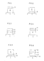
- Fig. l shows a photosensitive member of one type comprising an electrically conductive substrate l, a charge transporting layer 2 formed on the substrate and a charge generating layer 3 formed on the layer 2.
- Fig. 2 shows another type comprising an electrically conductive substrate l, a charge generating layer 3 on the substrate and a charge transporting layer 2 on the layer 3.
- Fig. 3 shows another type comprising an electrically conductive substrate l, and a charge transporting layer 2, a charge generating layer 3 and another charge transporting layer 2 formed over the substrate and arranged one over another.
- photosensitive members are used, for example, by positively charging the surface with a corona charger or the like and exposing the charged surface to an optical image.
- the holes then generated in the charge generating layer 3 travel through the charge transporting layer 2 toward the substrate l.
- the electrons generated in the charge generating layer 3 travel through the charge transporting layer 2 toward the surface of the photosensitive member.
- the holes generated in the charge generating layer 3 travel through the lower charge transporting layer 2 toward the substrate l, and at the same time, the electrons generated in the charge generating layer 3 travel through the upper transporting layer 2 toward the surface of the member. Consequently, an electrostatic latent image is formed, with satisfactory light decay assured.
- the electron and the hole may be replaced by each other in respect of the above behavior for the interpretation ot the travel of carriers.
- the image projecting light passes through the charge transporting layer, which nevertheless has high transmittancy, permitting satisfactory formation of latent image.
- Fig. 4 shows another type comprising an electrically conductive substrate l, and a charge transporting layer 2, a charge generating layer 3 and a charge transporting layer 4 provided over the substrate and arranged one over another.
- the illustrated structure corresponds to the structure of Fig. l provided with a surface protective layer. Since the outermost surface of the structure of Fig. l is provided by a charge generating of a-Si having poor humidity resistance in the present invention, it is generally desirable that the surface be covered with a protective layer for assuring stability toward humidity.
- the charge transporting layer embodying the invention and having high durability provides the outermost surface, so that the surface protective layer need not be provided.
- such a photosensitive member can be formed with a surface protective layer as another type so as to be compatible with various other elements within the copying machine, for example, to be free from surface soiling deposition of developer.
- Fig. 5 shows another type comprising an electrically conductive substrate l, and an intermediate layer 5, a charge generating layer 3 and a charge transporting layer 2 which are formed over the substrate and arranged one over another.
- this structure corresponds to the structure of Fig. 2 provided with an intermediate layer.
- a charge generating layer of a-Si is joined to the substrate in the structure of Fig. 2, it is generally desirable to interpose an intermediate layer therebetween to assure good adhesion and an injection inhibitory effect.
- the charge transporting layer of the invention which is excellent in adhesion and injection inhibitory effect is joined to the substrate, so that no intermediate layer may be provided.
- the photosensitive member of either of these types can be formed with an intermediate layer in order to render the transporting layer to be formed compatible with the preceding fabrication step, such as pretreatment of the conductive substrate. Another type of photosensitive member is then available.
- Fig. 6 shows still another type comprising an electrically conductive substrate l, and an intermediate layer 5, a charge transporting layer 2, a charge generating layer 3 and a surface protective layer 4 which are formed over the substrate and superposed one over another.
- this structure corresponds to the structure of Fig. l provided with an intermediate layer and a surface protective layer.
- the intermediate and protective layers are formed for the same reasons as already stated.
- the provision of these two layers in the structure of Fig. 2 or 3 affords another type.
- the intermediate layer and the surface protective layer are not limited specifically in material or fabrication process. Any material or process is suitably selectable provided that the contemplated object can be achieved.
- the a-C layer of the invention may be used. However, if the material to be used is an insulating material such as one already mentioned, the thickness of the layer needs to be up to 5 microns to preclude occurrence of residual potential.
- the charge transporting layer of the photosensitive member embodying the present invention is produced by so-called plasma polymerization wherein molecules is a vapor phase are subjected to discharge decomposition in a vacuum phase, and the active neutral seeds or charge seeds contained in the resulting atmosphere of plasma are led onto a substrate by diffusion or an electric or magnetic force and accumulated into a solid phase on the substrate through a rebinding reaction.
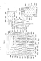
- Fig. 7 shows an apparatus for preparing the photosensitive member of the invention.
- First to sixth tanks 70l to 706 have enclosed therein starting material compounds which are in gas phase at room temperature and a carrier gas and are connected respectively to first to sixth regulator valves 707 to 7l2 and first to sixth flow controllers 7l3 to 7l8.
- First to third containers 7l9 to 72l contain starting material compounds which are liquid or solid at room temperature, can be preheated by first to third heaters 722 to 724 for vaporizing the compounds, and are connected to seventh to ninth regulator valves 725 to 727 and seventh to ninth flow controllers 728 to 730, respectively.
- the gases to be used as selected from among these gases are mixed together by a mixer 73l and fed to a reactor 733 via a main pipe 732.
- the interconnecting piping can be heated by a pipe heater 734 which is suitably disposed so that the material compound, in a liquid or solid phase at room temperature and vaporized by preheating, will not condense during transport.
- a grounded electrode 735 and a power application electrode 736 are arranged as opposed to each other within the reactor 733. Each of these electrodes can be heated by an electrode heater 737.
- the power application electrode 736 is connected to a high-frequency power source 739 via a high-frequency power matching device 738, to a low-frequency power source 74l via a low-frequency power matching device 740 and to a d.c. power source 743 via a low-pass filter 742.
- the internal pressure of the reactor 733 is adjustable by a pressure control valve 745.
- the reactor 733 is evacuated by a diffusion pump 747 and an oil rotary pump 748 via an exhaust system selecting valve 746, or by a cooling-removing device 749, a mechanical booster pump 750 and an oil rotary pump 748 via another exhaust system selecting value 746.
- the exhaust gas is further made harmless by a suitable removal device 753 and then released to the atmosphere.
- the evacuation piping system can also be heated by a suitably disposed pipe heater 734 so that the material compound which is liquid or solid at room temperature and vaporized by preheating will not condense during transport.
- the reactor 733 can also be heated by a reactor heater 75l.
- An electrically conductive substrate 752 is placed on the electrode 735 in the reactor.
- Fig. 7 shows that the substrate 752 is fixed to the grounded electrode 735, the substrate may be attached to the power application electrode 736, or to both the electrodes.
- Fig. 8 shows another type of apparatus for preparing the photosensitive member of the invention.
- This apparatus has the same construction as the apparatus of Fig. 7 with the exception of the interior arrangement of the reactor 833.
- the numerals shown by 700 order in Fig. 7 are replaced by the numerals at 800 order in Fig. 8.
- the reactor 833 is internally provided with a hollow cylindrical electrically conductive substrate 852 serving also as the grounded electrode 735 of Fig. 7 and with an electrode heater 837 inside thereof.
- a power application electrode 836 similarly in the form of a hollow cylinder, is provided around the substrate 852 and surrounded by an electrode heater 837.
- the conductive substrate 852 is rotatable about its own axis by motor from outside.
- the reactor for preparing the photosensitive member is first evacuated by the diffusion pump to a vacuum of about l0 ⁇ 4 to about l0 ⁇ 6 torr, whereby the adsorbed gas inside the reactor is removed.
- the reactor is also checked for the degree of vacuum.
- the electrodes and the substrate fixedly placed on the electrode are heated to a predetermined temperature.
- an undercoat layer or a charge generating layer may be formed on the substrate before the charge transporting layer is formed when so required.
- the undercoat or charge generating layer may be formed by the present apparatus or by some other apparatus.
- material gases are fed into the reactor from the first to sixth tanks and the first to third containers (i.e.
- the flow controllers concerned i.e. first to ninth flow controllers and the interior of the reactor is maintained in a predetermined vacuum by the pressure control valve.
- the high-frequency power source for example, is selected by the connection selecting switch to apply a high-frequency power to the power application electrode. This initiates discharge across the two electrodes, forming a solid layer on the substrate with time. The thickness of the layer is controllable by varying the reaction time, such that the discharge is discontinued upon the thickness reaching the desired value.
- any a-Si layer or a-C layer can be formed as desired by using suitable selected material gases.
- the layers, which are different in composition can be formed as a laminate structure by temporarily discontinuing the discharge after forming one of the layers to change the composition of material gases, and then restarting the discharge to form the other layer over the first layer. Further, it is possible to form the layers having different in the form of a laminate structrue having a gradient composition by gradually changing only the flow rates of material gases with continued discharge.
- the thickness of each layer is controlled by varying the reaction time. Then, the photosensitive member of the present invention is prepared by discontinuing the discharge when the desired laminate structure is obtained with the thickness of each layer thus controlled.
- the regulator valves concerned are closed, and the reactor is thoroughly exhausted.
- a photosensitive member of the desired structure hss been formed according to the invention
- the vacuum within the reactor is vitiated and the member is removed from the reactor.
- another charge generating layer or overcoat layer are to be superposed on the above structure, such a layer is formed using the present apparatus as it is.
- the photosensitive member formed by the above process is taken out from the reaction chamber after destroying the vacuum, and is then transferred to another apparatus to form such a layer.
- the photosensitive member of the present invention can be obtained which has a charge transporting layer and a charge generating layer and, if necessary, an overcoat layer.
- a photosensitive member was prepared, the member comprising an electrically conductive substrate, a charge transporting layer and a charge generating layer provided in this order as shown in Fig. l.
- CTL Charge Transporting Layer Forming Step
- the glow discharge decomposition apparatus shown in Fig. 7 was used. First, the interior of the reactor 733 was evacuated to a high vacuum of about l0 ⁇ 6 torr, and the first and second regulator valves 707 and 708 were thereafter opened to introduce hydrogen gas from the first tank 70l into the first flow controller 7l3 and acetylene gas from the second tank 702 into the second flow controller 7l4, each at an output pressure of l.0 kg/cm2. The dials on the flow controllers were adjusted to supply the hydrogen gas at a flow rate of l00 sccm and the acetylene gas at 30 sccm to the reactor 733 through the main pipe 732 via the intermediate mixer 73l.
- the internal pressure of the reactor 733 was adjusted to l.5 torr by the pressure control valve 745.
- the substrate 752 which was an aluminum substrate measuring 50 mm in length, 50 mm in width and 3 mm in thickness, was preheated to 200°C.
- the a-C layer thus obtained was found to contain 30 atomic % of hydrogen atoms based on the combined amount of carbon atoms and hydrogen atoms.
- the tanks were partly exchanged and the first, second and sixth regulator valves 707, 708 and 7l2 were opened to introduce hydrogen gas from the first tank 70l into the first flow controller 7l3, germane gas from the second tank 702 into the second flow controller 7l4 and silane gas from the sixth tank 706 into the sixth flow controller 7l8, each at an output pressure of l.0 kg/cm2.
- the dials on the flow controllers were adjusted to supply the hydrogen gas at a flow rate of 200 sccm, germane gas at a flow rate of 0.6 sccm and the silane gas at l00 sccm to the reactor 733.
- the internal pressure of the reactor 733 was adjusted to 0.8 torr by the pressure control valve 745.
- the substrate 752 formed with the a-C layer was preheated to 250°C.
- 35-watt power with a frequency of l3.56 MHz was applied to the power application electrode 736 from the high-frequency power source 739 to effect glow discharge for 5 minutes, whereby a charge generating a-Si:H layer was formed with a thickness of 0.3 microns.
- the a-Si layer thus obtained was found to contain 20 atomic % of hydrogen atoms and l atomic % of germanium atoms based on all the constituent atoms therein.
- the photosensitive member obtained When the photosensitive member obtained was used for the usual Carlson process with negative charging and positive charging, the member showed a maximum charge potential (hereinafter referred to as Vmax) of -3l0V (+380V). (The obtained values at positive charging were shown in parenthesis hereinafter). Specifically, the chargeability per l micron (hereinafter referred to as C.A.) was 20V/micron (25V/micron) by calculating from the entire thickness of the member, i.e. l5.3 microns, indicating that the member had satisfactory charging properties.
- Vmax maximum charge potential
- C.A. chargeability per l micron
- the period of time required for dark decay from Vmax to the potential corresponding to 90 % of Vmax (hereinafter referred to as DDR) was about 6 seconds (8 seconds), showing that the member has satisfactory charge retentivity.
- the amount of light required for the light decay from Vmax to the potential corresponding to 20 % of Vmax with white light was about 2.6 lux-sec (3.3 lux-sec), showing that the member was satisfactory in photosensitive characteristics.
- Photosensitive members were prepared as similarly as with Example l, each member comprising an electrically conductive substrate (l), a charge transporting layer (2) and a charge generating layer (3) provided in this order as shown in Fig. l.
- Table l shows the various condition values for forming a charge transporting layer
- Table 2 shows the various condition values for forming a charge generating layer
- Talbe 3 shows the results of the evaluation of each member.
- Table l and Table 2 show the conditions different from Example l for forming a charge trasnporting layer and charge generating layer and classified into 34 items (l) to (34). These items are described at the top column of each Table. Some condition values shown at each item are common to each example, while others are varying in each example.
- Table l shows the items (l) to (l6) as follows:
- Table 2 shows the items (l7) to (34) as follows:
- the level of the clearness of the image is represented by o (clear) and x (unclear). More specifically, the photosensitive members marked with x are not satisfactory in performance. When such members were used in the Carlson process for forming images thereon, followed by image transfer, fogged copy images only were obtained.
- the charge transporting layers of Examples l to 32 comprise amorphous carbon containing hydrogen.
- Table 4 shows the outline of the photosensitive members prepared by Examples l to 32.
- Photosensitive members were prepared, the members comprising an electrically conductive substrate (l), a charge transporting layer (2) and a charge generating layer (3) provided in this order as shown in Fig. l.
- Table 5 The respective condition values for forming a charge transporting layer and a charge generating layer are shown in Table 5 and Table 6.
- Table 7 indicates the results of the evaluation of each member.
- Photosensitive members were prepared as similarly as with Example l, each member comprising an electrically conductive substrate (l), a charge transporting layer (2) and a charge generating layer (3) provided in this order as shown in Fig. l.
- Table 8 shows the various condition values for forming a charge transporting layer
- Table 9 shows the various condition values for forming a charge generating layer
- Talbe l0 shows the results of the evaluation of each member.
- the charge transporting layers of Examples 33 to 64 comprise amorphous carbon containing hydrogen and halogen.
- Table ll shows the outline of the photosensitive members prepared by Examples 33 to 64.
- Photosensitive members were prepared, the members comprising an electrically conductive substrate (l), a charge transporting layer (2) and a charge generating layer (3) provided in this order as shown in Fig. l.
- Table l2 The respective condition values for forming a charge transporting layer and a charge generating layer are shown in Table l2 and Table l3.
- Table l4 indicates the results of the evaluation of each member.
Landscapes
- Chemical & Material Sciences (AREA)
- Inorganic Chemistry (AREA)
- Physics & Mathematics (AREA)
- General Physics & Mathematics (AREA)
- Photoreceptors In Electrophotography (AREA)
Applications Claiming Priority (20)
| Application Number | Priority Date | Filing Date | Title |
|---|---|---|---|
| JP22944386A JPS6382471A (ja) | 1986-09-26 | 1986-09-26 | 感光体 |
| JP229380/86 | 1986-09-26 | ||
| JP22938086A JPS6381474A (ja) | 1986-09-26 | 1986-09-26 | 感光体 |
| JP22937586A JPS6381469A (ja) | 1986-09-26 | 1986-09-26 | 感光体 |
| JP229372/86 | 1986-09-26 | ||
| JP22945086A JPS6382478A (ja) | 1986-09-26 | 1986-09-26 | 感光体 |
| JP229451/86 | 1986-09-26 | ||
| JP22937186A JPS6381465A (ja) | 1986-09-26 | 1986-09-26 | 感光体 |
| JP22937686A JPS6381470A (ja) | 1986-09-26 | 1986-09-26 | 感光体 |
| JP22937286A JPS6381466A (ja) | 1986-09-26 | 1986-09-26 | 感光体 |
| JP22944486A JPS6382472A (ja) | 1986-09-26 | 1986-09-26 | 感光体 |
| JP229444/86 | 1986-09-26 | ||
| JP229376/86 | 1986-09-26 | ||
| JP229379/86 | 1986-09-26 | ||
| JP22945186A JPS6382479A (ja) | 1986-09-26 | 1986-09-26 | 感光体 |
| JP22937986A JPS6381473A (ja) | 1986-09-26 | 1986-09-26 | 感光体 |
| JP229450/86 | 1986-09-26 | ||
| JP229443/86 | 1986-09-26 | ||
| JP229371/86 | 1986-09-26 | ||
| JP229375/86 | 1986-09-26 |
Publications (2)
| Publication Number | Publication Date |
|---|---|
| EP0261654A2 true EP0261654A2 (de) | 1988-03-30 |
| EP0261654A3 EP0261654A3 (de) | 1989-11-23 |
Family
ID=27580426
Family Applications (1)
| Application Number | Title | Priority Date | Filing Date |
|---|---|---|---|
| EP87113883A Withdrawn EP0261654A3 (de) | 1986-09-26 | 1987-09-23 | Lichtempfindliches Element mit ladungserzeugender Schicht und Ladungstransportschicht |
Country Status (1)
| Country | Link |
|---|---|
| EP (1) | EP0261654A3 (de) |
Cited By (1)
| Publication number | Priority date | Publication date | Assignee | Title |
|---|---|---|---|---|
| EP0408966A3 (en) * | 1989-07-19 | 1991-04-24 | Siemens Aktiengesellschaft | Electrophotographic recording material and process for its manufacture |
Family Cites Families (3)
| Publication number | Priority date | Publication date | Assignee | Title |
|---|---|---|---|---|
| DE3200376A1 (de) * | 1981-01-09 | 1982-11-04 | Canon K.K., Tokyo | Fotoleitfaehiges element |
| JPS5912448A (ja) * | 1982-07-12 | 1984-01-23 | Ricoh Co Ltd | 電子写真用感光体 |
| JPS6012554A (ja) * | 1983-07-04 | 1985-01-22 | Fuji Photo Film Co Ltd | 電子写真用感光体 |
-
1987
- 1987-09-23 EP EP87113883A patent/EP0261654A3/de not_active Withdrawn
Cited By (1)
| Publication number | Priority date | Publication date | Assignee | Title |
|---|---|---|---|---|
| EP0408966A3 (en) * | 1989-07-19 | 1991-04-24 | Siemens Aktiengesellschaft | Electrophotographic recording material and process for its manufacture |
Also Published As
| Publication number | Publication date |
|---|---|
| EP0261654A3 (de) | 1989-11-23 |
Similar Documents
| Publication | Publication Date | Title |
|---|---|---|
| US4797338A (en) | Photosensitive member comprising charge generating layer and charge transporting layer | |
| US4863821A (en) | Photosensitive member comprising charge generating layer and charge transporting layer having amorphous carbon | |
| US4886724A (en) | Photosensitive member having an overcoat layer and process for manufacturing the same | |
| US4871632A (en) | Photosensitive member comprising charge generating layer and charge transporting layer | |
| US4810606A (en) | Photosensitive member comprising charge generating layer and charge transporting layer | |
| US4851313A (en) | Photosensitive member comprising charge generating layer and charge transporting layer and process for preparing same | |
| EP0261654A2 (de) | Lichtempfindliches Element mit ladungserzeugender Schicht und Ladungstransportschicht | |
| US4891292A (en) | Photosensitive member having an amorphous carbon overcoat layer | |
| US4876168A (en) | Photosensitive member comprising charge generating layer and charge transporting layer comprising amorphous carbon containing chalogen or transition metal | |
| US4868076A (en) | Photosensitive member comprising charge generating layer and charge transporting layer | |
| EP0261651A1 (de) | Lichtempfindliches Element, das eine Ladungserzeugungsschicht und eine Ladungstransportschicht enthält | |
| EP0261652A2 (de) | Lichtempfindliches Element mit ladungserzeugender Schicht und eine Ladungstransportschicht | |
| US4902595A (en) | Photosensitive member having an overcoat lyer and process for manufacturing the same | |
| US4891291A (en) | Photosensitive member having an amorphous carbon overcoat layer | |
| JPS6381446A (ja) | 感光体 | |
| JPS63218961A (ja) | 感光体 | |
| JPS6373261A (ja) | 感光体 | |
| JPS6381461A (ja) | 感光体 | |
| JPS6314157A (ja) | 感光体 | |
| JPS63309965A (ja) | 感光体 | |
| JPS6382479A (ja) | 感光体 | |
| JPS6381478A (ja) | 感光体 | |
| JPS63218962A (ja) | 感光体 | |
| JPS6381482A (ja) | 感光体 | |
| JPS62299973A (ja) | 感光体 |
Legal Events
| Date | Code | Title | Description |
|---|---|---|---|
| PUAI | Public reference made under article 153(3) epc to a published international application that has entered the european phase |
Free format text: ORIGINAL CODE: 0009012 |
|
| AK | Designated contracting states |
Kind code of ref document: A2 Designated state(s): DE FR GB |
|
| PUAL | Search report despatched |
Free format text: ORIGINAL CODE: 0009013 |
|
| AK | Designated contracting states |
Kind code of ref document: A3 Designated state(s): DE FR GB |
|
| STAA | Information on the status of an ep patent application or granted ep patent |
Free format text: STATUS: THE APPLICATION IS DEEMED TO BE WITHDRAWN |
|
| 18D | Application deemed to be withdrawn |
Effective date: 19900525 |
|
| RIN1 | Information on inventor provided before grant (corrected) |
Inventor name: HOTOMI, HIDEO Inventor name: IINO, SYUJI Inventor name: OSAWA, IZUMI |