EP0261739B1 - Amplificateur de contrôle - Google Patents
Amplificateur de contrôle Download PDFInfo
- Publication number
- EP0261739B1 EP0261739B1 EP87201816A EP87201816A EP0261739B1 EP 0261739 B1 EP0261739 B1 EP 0261739B1 EP 87201816 A EP87201816 A EP 87201816A EP 87201816 A EP87201816 A EP 87201816A EP 0261739 B1 EP0261739 B1 EP 0261739B1
- Authority
- EP
- European Patent Office
- Prior art keywords
- transistor
- resistor
- amplifier
- collector
- current
- Prior art date
- Legal status (The legal status is an assumption and is not a legal conclusion. Google has not performed a legal analysis and makes no representation as to the accuracy of the status listed.)
- Expired - Lifetime
Links
- 230000003071 parasitic effect Effects 0.000 claims description 4
- 230000000694 effects Effects 0.000 claims 1
- 230000003287 optical effect Effects 0.000 description 4
- 239000003990 capacitor Substances 0.000 description 2
- 230000005540 biological transmission Effects 0.000 description 1
- 230000001419 dependent effect Effects 0.000 description 1
Images
Classifications
-
- H—ELECTRICITY
- H03—ELECTRONIC CIRCUITRY
- H03G—CONTROL OF AMPLIFICATION
- H03G1/00—Details of arrangements for controlling amplification
- H03G1/0005—Circuits characterised by the type of controlling devices operated by a controlling current or voltage signal
- H03G1/0017—Circuits characterised by the type of controlling devices operated by a controlling current or voltage signal the device being at least one of the amplifying solid-state elements
- H03G1/0023—Circuits characterised by the type of controlling devices operated by a controlling current or voltage signal the device being at least one of the amplifying solid-state elements in emitter-coupled or cascode amplifiers
Definitions
- Control amplifiers are used for the automatic compensation of telephone cable attenuation, or in receivers of broadband optical systems for the automatic compensation of length and broadband optical systems for the automatic compensation of length and temperature-dependent attentuation of optical links in a optical transmission system. In this type of amplifier, bandwidth must usually be sacrificed at the expense of control range.
- a known control amplifier is described in EP-A 0152151.
- a series arrangement of two resistors is provided between the output of this amplifier and a point of constant potential.
- the collector of one transistor is coupled to the output and the collector of the other transistor is coupled to the junction of the two resistors.
- the magnitude of the control range of this prior art amplifier is determined by the resistance values of the two resistors and is equal to
- A is the control range
- R(1) is the resistance value of the resistor connected to the point of constant potential
- R(2) is the resistance value of the resistor connected to the output of the amplifier.
- the maximum value of R(2) is limited by the collector capacitance of the other transistor, this capacitance also determining the maximum frequency at which the amplifier is still suitable for use.
- a further limiting factor is the minimal value of R(1).
- the resistor connected to the point of constant potential has a parasitic inductance, as a result of which the output voltage of the amplifier will increase versus an increasing frequency, when the impedance of the parasitic inductance is not small with respect to R(1).
- R(1) 10 ⁇
- the invention has for its object to provide measures by means of which the maximum control range can be increased at an unchanged bandwidth.
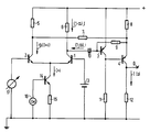
- the collector of the transistor 1 is connected to a point of constant potential via a resistor 6 and, via the capacitance 10 to the input of a dual-stage negatively feedback amplifier, constituted by the transistors 3 and 4.
- the base of the transistor 1 is connected to ground via the d.c. voltage source 13.
- the emitter of the transistor 1 is connected to the emitter of the transistor 2, this base being connected to ground via a control voltage source.
- the collector of the transistor 2 is connected to a point of constant potential via the resistor 5 and to the emitter of transistor 4 of the two-stage amplifier via the resistor 7.
- the emitters of the transistors 1 and 2 are connected to ground via the series arrangement of the main current path of the transistor 14 and the resistor 15.
- the base of the transistor 14 is connected to ground via the signal voltage source 16.
- the emitter of the transistor 3 is connected to a point of constant potential.
- the collector of the transistor 3 is connected to ground via the resistor 11 and also to the base of the transistor 4, whose collector is connected to ground via the resistor 12 and to the output 0 of the two stage amplifier.
- the emitter of the transistor 4 is connected to a point of constant potential via the resistor 8.
- the base of the transistor 3 is connected to the emitter of the transistor 4 via the resistor 9.
- the current distribution factor ⁇ is set, where 0 ⁇ 1. This causes a direct current having a value ⁇ .I to flow through the main current path of the transistor 2 and a direct current having a value (1- ⁇ ).I to flow through the main current path of the transistor 1.
- a signal current having a value ⁇ .i also flows through the main current path of the transistor 2 and a signal current having a value (1- ⁇ ).i flows through the main current path of the transistor 1.
- the values of the currents I and i are determined by the voltage produced by the input signal source 16 in combination with the value of the resistor 15. Since the input impedance of the amplifier formed by the transistors 3 and 4 is much less than the value of the resistor 6, substantially all the signal current flowing in the main current path of the transistor will flow through the said input impedance via the capacitor 10.
- the control amplifier has the advantage that the impedances with which the collectors of the transistors 1 and 2 are terminated are low-resistance impedances, so that the influence of the collector capacitances on the bandwidth is much smaller.
- An additional advantage is that a parasitic inductance of the resistor 5 can be compensated for by including such an inductance in series with the resistor 7 that splitting the current through the resistors 5 and 7 does not depend on the frequency. This is possible when R(5) + R(7) > R(8) .
Landscapes
- Amplifiers (AREA)
- Control Of Amplification And Gain Control (AREA)
- Networks Using Active Elements (AREA)
Claims (1)
- Un amplificateur de commande ayant un premier étage amplificateur comprenant un premier transistor (1) et un second transistor (2) dont les émetteurs sont connectés à une première borne d'une source de courant de signal commune (14, 15, 16), dont une seconde borne est connectée à un point de potentiel constant, une source de tension de commande (17) étant placée entre les électrodes de base des premier et second transistors, et le collecteur des premier et second transistors étant connecté à un point de potentiel constant par l'intermédiaire d'au moins une première résistance (6) et une seconde résistance (5), respectivement, et un second étage amplificateur (3, 4, 9, 8, 11, 12) comprenant un transistor de sortie (4), le collecteur du premier transistor (1) étant connecté à l'entrée du second étage amplificateur et le collecteur du second transistor (2) étant connecté à l'émetteur du transistor de sortie par l'intermédiaire d'au moins une troisième résistance (7), de façon qu'une fraction du courant de collecteur du second transistor circule, par l'intermédiaire de la troisième résistance, vers l'émetteur du transistor de sortie, et le collecteur de ce transistor de sortie constituant la sortie de l'amplificateur de commande, CARACTERISE EN CE QUE le second étage amplificateur est un amplificateur de courant, et en ce que la fraction précitée du courant de collecteur est rendue indépendante de la fréquence par l'inclusion d'une inductance en série avec la troisième résistance, qui compense les effets de l'inductance parasite inévitable de la seconde résistance.
Applications Claiming Priority (2)
| Application Number | Priority Date | Filing Date | Title |
|---|---|---|---|
| NL8602409A NL8602409A (nl) | 1986-09-24 | 1986-09-24 | Regelbare versterker. |
| NL8602409 | 1986-09-24 |
Publications (2)
| Publication Number | Publication Date |
|---|---|
| EP0261739A1 EP0261739A1 (fr) | 1988-03-30 |
| EP0261739B1 true EP0261739B1 (fr) | 1993-07-21 |
Family
ID=19848584
Family Applications (1)
| Application Number | Title | Priority Date | Filing Date |
|---|---|---|---|
| EP87201816A Expired - Lifetime EP0261739B1 (fr) | 1986-09-24 | 1987-09-22 | Amplificateur de contrôle |
Country Status (5)
| Country | Link |
|---|---|
| US (1) | US4825176A (fr) |
| EP (1) | EP0261739B1 (fr) |
| JP (1) | JP2515821B2 (fr) |
| DE (1) | DE3786627T2 (fr) |
| NL (1) | NL8602409A (fr) |
Families Citing this family (2)
| Publication number | Priority date | Publication date | Assignee | Title |
|---|---|---|---|---|
| DE2701624C2 (de) * | 1977-01-17 | 1983-03-17 | Westfalia Separator Ag, 4740 Oelde | Kontinuierlich arbeitende Schleudertrommel zum Konzentrieren auspendierter Feststoffe |
| US5631598A (en) * | 1995-06-07 | 1997-05-20 | Analog Devices, Inc. | Frequency compensation for a low drop-out regulator |
Family Cites Families (8)
| Publication number | Priority date | Publication date | Assignee | Title |
|---|---|---|---|---|
| US886006A (en) * | 1907-07-19 | 1908-04-28 | John E Gunther | Seed-separator. |
| DE1816034B2 (de) * | 1968-12-20 | 1975-07-03 | Philips Patentverwaltung Gmbh, 2000 Hamburg | Regelbare Verstärkerstufe |
| UST886006I4 (en) | 1970-04-15 | 1971-05-04 | Linear pour-quadrant multiplier | |
| NL166162C (nl) * | 1971-05-14 | 1981-06-15 | Philips Nv | Versterkerschakeling met regelbare versterking. |
| US3891937A (en) * | 1972-12-21 | 1975-06-24 | Philips Corp | Circuit arrangement for electronic gain/control, in particular electronic volume control circuit |
| JPS54147761A (en) * | 1978-05-12 | 1979-11-19 | Hitachi Ltd | Gain control unit |
| NL8100929A (nl) * | 1981-02-26 | 1982-09-16 | Philips Nv | Optische ontvanger. |
| NL8400463A (nl) * | 1984-02-14 | 1985-09-02 | Philips Nv | Breedband regelversterker. |
-
1986
- 1986-09-24 NL NL8602409A patent/NL8602409A/nl not_active Application Discontinuation
-
1987
- 1987-09-22 DE DE87201816T patent/DE3786627T2/de not_active Expired - Fee Related
- 1987-09-22 EP EP87201816A patent/EP0261739B1/fr not_active Expired - Lifetime
- 1987-09-22 JP JP62236435A patent/JP2515821B2/ja not_active Expired - Lifetime
- 1987-09-23 US US07/099,944 patent/US4825176A/en not_active Expired - Lifetime
Non-Patent Citations (1)
| Title |
|---|
| A. B. GREBENE: Bipolar and MOS analog integrated circuit design", 1984, Wiley, New York, US, pages 400-405 * |
Also Published As
| Publication number | Publication date |
|---|---|
| US4825176A (en) | 1989-04-25 |
| EP0261739A1 (fr) | 1988-03-30 |
| DE3786627D1 (de) | 1993-08-26 |
| JPS63133709A (ja) | 1988-06-06 |
| JP2515821B2 (ja) | 1996-07-10 |
| NL8602409A (nl) | 1988-04-18 |
| DE3786627T2 (de) | 1993-11-04 |
Similar Documents
| Publication | Publication Date | Title |
|---|---|---|
| US6864750B2 (en) | Cascode distributed amplifier | |
| US4764732A (en) | Switchable mode amplifier for wide dynamic range | |
| JP2538938B2 (ja) | 光前置増幅器 | |
| US4491802A (en) | Wide-band amplifier system | |
| US4998012A (en) | Fiber optic transimpedance receiver | |
| US4719374A (en) | Broadband electric field controlled switching circuit | |
| EP0151532A2 (fr) | Atténuateur à diodes, commandé par tension | |
| EP0788223B1 (fr) | Atténuateur variable à diodes Pin | |
| US4395643A (en) | Broadband circuit with rapidly variable resistor | |
| US4956615A (en) | Input circuit for high-frequency amplifiers | |
| US4507615A (en) | Non-linear amplifier systems | |
| EP0261739B1 (fr) | Amplificateur de contrôle | |
| KR900006294B1 (ko) | 광전변환회로 | |
| EP0066401B1 (fr) | Amplificateur non-linéaire à réaction positive | |
| KR0166362B1 (ko) | 광대역 신호 증폭기 | |
| EP1500190B1 (fr) | Circuit amplificateur electronique | |
| JPH10126179A (ja) | 利得制御回路及び方法 | |
| US3437947A (en) | Signal amplifier having grounded-base stage for a cable terminating impedance | |
| US4405903A (en) | Variolosser for an automatic gain control circuit | |
| US4663583A (en) | Automatically variable phase characteristic all-pass circuit | |
| EP0152151B1 (fr) | Amplificateur commandé à bande large | |
| EP0406865A2 (fr) | Circuit de démodulation | |
| CA1283463C (fr) | Amplificateur a grande dynamique a modes commutables | |
| JPS5834631A (ja) | チュ−ナ装置 | |
| CA2025817A1 (fr) | Amplificateur commutable a gamme dynamique etendue |
Legal Events
| Date | Code | Title | Description |
|---|---|---|---|
| PUAI | Public reference made under article 153(3) epc to a published international application that has entered the european phase |
Free format text: ORIGINAL CODE: 0009012 |
|
| AK | Designated contracting states |
Kind code of ref document: A1 Designated state(s): DE FR GB NL SE |
|
| 17P | Request for examination filed |
Effective date: 19880920 |
|
| 17Q | First examination report despatched |
Effective date: 19900912 |
|
| RAP1 | Party data changed (applicant data changed or rights of an application transferred) |
Owner name: AT&T NETWORK SYSTEMS INTERNATIONAL B.V. Owner name: APT NEDERLAND B.V. |
|
| RAP3 | Party data changed (applicant data changed or rights of an application transferred) |
Owner name: AT&T NETWORK SYSTEMS INTERNATIONAL B.V. Owner name: AT&T NETWORK SYSTEMS NEDERLAND B.V. |
|
| GRAA | (expected) grant |
Free format text: ORIGINAL CODE: 0009210 |
|
| AK | Designated contracting states |
Kind code of ref document: B1 Designated state(s): DE FR GB NL SE |
|
| REF | Corresponds to: |
Ref document number: 3786627 Country of ref document: DE Date of ref document: 19930826 |
|
| ET | Fr: translation filed | ||
| PLBE | No opposition filed within time limit |
Free format text: ORIGINAL CODE: 0009261 |
|
| STAA | Information on the status of an ep patent application or granted ep patent |
Free format text: STATUS: NO OPPOSITION FILED WITHIN TIME LIMIT |
|
| 26N | No opposition filed | ||
| EAL | Se: european patent in force in sweden |
Ref document number: 87201816.3 |
|
| PGFP | Annual fee paid to national office [announced via postgrant information from national office to epo] |
Ref country code: SE Payment date: 20000620 Year of fee payment: 14 |
|
| PGFP | Annual fee paid to national office [announced via postgrant information from national office to epo] |
Ref country code: FR Payment date: 20000823 Year of fee payment: 14 |
|
| PGFP | Annual fee paid to national office [announced via postgrant information from national office to epo] |
Ref country code: GB Payment date: 20000825 Year of fee payment: 14 |
|
| PGFP | Annual fee paid to national office [announced via postgrant information from national office to epo] |
Ref country code: NL Payment date: 20000914 Year of fee payment: 14 |
|
| PGFP | Annual fee paid to national office [announced via postgrant information from national office to epo] |
Ref country code: DE Payment date: 20000929 Year of fee payment: 14 |
|
| PG25 | Lapsed in a contracting state [announced via postgrant information from national office to epo] |
Ref country code: GB Free format text: LAPSE BECAUSE OF NON-PAYMENT OF DUE FEES Effective date: 20010922 |
|
| PG25 | Lapsed in a contracting state [announced via postgrant information from national office to epo] |
Ref country code: SE Free format text: LAPSE BECAUSE OF NON-PAYMENT OF DUE FEES Effective date: 20010923 |
|
| REG | Reference to a national code |
Ref country code: GB Ref legal event code: IF02 |
|
| PG25 | Lapsed in a contracting state [announced via postgrant information from national office to epo] |
Ref country code: NL Free format text: LAPSE BECAUSE OF NON-PAYMENT OF DUE FEES Effective date: 20020401 |
|
| PG25 | Lapsed in a contracting state [announced via postgrant information from national office to epo] |
Ref country code: DE Free format text: LAPSE BECAUSE OF NON-PAYMENT OF DUE FEES Effective date: 20020501 |
|
| EUG | Se: european patent has lapsed |
Ref document number: 87201816.3 |
|
| GBPC | Gb: european patent ceased through non-payment of renewal fee |
Effective date: 20010922 |
|
| PG25 | Lapsed in a contracting state [announced via postgrant information from national office to epo] |
Ref country code: FR Free format text: LAPSE BECAUSE OF NON-PAYMENT OF DUE FEES Effective date: 20020531 |
|
| NLV4 | Nl: lapsed or anulled due to non-payment of the annual fee |
Effective date: 20020401 |
|
| REG | Reference to a national code |
Ref country code: FR Ref legal event code: ST |
|
| NLV4 | Nl: lapsed or anulled due to non-payment of the annual fee |
Effective date: 20020401 |