EP0262477A2 - Disposition de circuit pour la transmission de signaux de données - Google Patents
Disposition de circuit pour la transmission de signaux de données Download PDFInfo
- Publication number
- EP0262477A2 EP0262477A2 EP87113200A EP87113200A EP0262477A2 EP 0262477 A2 EP0262477 A2 EP 0262477A2 EP 87113200 A EP87113200 A EP 87113200A EP 87113200 A EP87113200 A EP 87113200A EP 0262477 A2 EP0262477 A2 EP 0262477A2
- Authority
- EP
- European Patent Office
- Prior art keywords
- address
- peripheral devices
- devices
- peripheral
- central control
- Prior art date
- Legal status (The legal status is an assumption and is not a legal conclusion. Google has not performed a legal analysis and makes no representation as to the accuracy of the status listed.)
- Withdrawn
Links
Images
Classifications
-
- G—PHYSICS
- G06—COMPUTING OR CALCULATING; COUNTING
- G06F—ELECTRIC DIGITAL DATA PROCESSING
- G06F12/00—Accessing, addressing or allocating within memory systems or architectures
- G06F12/02—Addressing or allocation; Relocation
- G06F12/06—Addressing a physical block of locations, e.g. base addressing, module addressing, memory dedication
- G06F12/0646—Configuration or reconfiguration
- G06F12/0669—Configuration or reconfiguration with decentralised address assignment
Definitions
- the invention relates to a circuit arrangement for transmitting data signals in the course of separate connections between a central control device and a plurality of peripheral devices connected to the latter via a shared circuit arrangement, each of which is permanently assigned a device address which is assigned to the respective peripheral device for in the course of a Establishing a connection and / or an existing connection and / or a connection clearing between it and the central control device to be processed control processes is available.
- the peripheral devices belonging to such a circuit arrangement generally have memory devices in which the device address assigned for the respective peripheral device is stored.
- memory devices for example, manually adjustable switches, read-only memories or loadable address registers used as address transmitters are suitable as storage devices.
- device addresses for peripheral devices are only determined by the assignment of device places within the circuit arrangement in question. This means that, in particular in the case of circuit arrangements having a large number of peripheral devices, a considerable amount of time is required on the part of the maintenance personnel before they are put into operation in order to assign them to the individual peripheral devices store the device addresses on them. Such a separate storage of device addresses must also always take place when peripheral devices are to be replaced.
- peripheral devices are each received by one of a plurality of receiving devices provided in connection with the mentioned line arrangement, each of which is permanently assigned an address which the respective peripheral device received by it is available as its device address.
- the invention has the advantage that, within a circuit arrangement, only one address is permanently assigned to each of the recording devices present in it, which address is available as the device address to the respectively recorded peripheral device.
- the addresses assigned to the receiving devices are addresses specific to the circuit arrangement, which can already be determined during the manufacture of the circuit arrangement. Since the peripheral devices receive device addresses supplied from the receiving devices, no separate devices for storing device addresses are required on the peripheral devices. This also eliminates the aforementioned setting processes or set-up processes on the peripheral devices when they are included in a special circuit arrangement.
- the receiving devices each consist of a connector arrangement, via which the respective peripheral device receives a hard-wired address as the device address via a predetermined number of plug contacts arranged in a separate area of the respective connector arrangement.
- This has the advantage that the connector arrangements can be assigned a location-dependent address, for example, within a subrack provided for accommodating peripheral devices, which address is supplied to the respective connector arrangement via a wiring frame provided in the subrack.
- the hard-wired addresses In order to occupy as few plug contacts as possible on the individual connector arrangements for the provision of a hard-wired address, it is expedient for the hard-wired addresses to be present in coded form on the separate plug contacts of the connector arrangements.
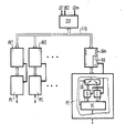
- a data signal transmission system is shown.
- This may be a data exchange system, for example.
- This data switching system has a central control device ZST with a large number of transmission lines UE1-UEm, which can be used either as subscriber lines for connecting data terminals or as exchange lines for connecting further data switching systems.
- the central control device ZST is also connected to a plurality of peripheral devices PE via a line arrangement Ltg consisting, for example, of a plurality of individual lines. These peripheral devices are each via a receiving device connected to the line arrangement.
- the recording devices are designated AV1-AVn in the drawing.
- These receiving devices are plug-in connector arrangements arranged in a subrack. An address dependent on their installation locations within the subrack is permanently assigned to these connector arrangements. This address is present in coded form on separate plug contacts of the respective connector arrangement, for example by supplying hard-wired logical potentials to these separate plug contacts in accordance with the selected coding.
- the separate contacts are otherwise arranged in an area designated AB in the drawing of the respective connector arrangement. The address at these separate plug contacts is, as will be explained in the following, fed to the peripheral device PE connected to the respective receiving device as its device address.
- the peripheral devices PE are conversion devices via which the central control device ZST is connected to further transmission lines for receiving or delivering data signals. Examples of such conversion devices are devices for converting the data signal format, devices for converting the transmission speed and devices for implementing the procedure. Such procedural implementations are required, for example, in the case of a transition between switching systems from switching networks operating with different transmission procedures, such as, for example, telex and teletex networks.
- the peripheral devices PE mentioned are identical in terms of their circuitry structure. For this reason, in the drawing this structure is only for the peripheral device connected to the receiving device AVn tion shown in sections.
- This peripheral device has a processing unit labeled VE, which controls the implementation and forwarding of it via the line arrangement Ltg or the data signals fed to it via the transmission line connected to it.
- This processing unit connects to the respective recording device, here towards the recording device AVn, a receiving device E serving for receiving data signals and a transmitting device S serving for the delivery of data signals.
- These two devices can be controlled from the processing unit VE via one control line each.
- Each of these devices also receives the address assigned to the respective recording device via the aforementioned separate plug contacts.
- a data selector DS which can be controlled by the processing unit VE is connected to the receiving device E and the transmitting device S. Controlled by the processing unit, this data selector optionally connects the receiving device E or the transmitting device S to the line arrangement Ltg for receiving or delivering data signals.
- the exchange of data signals between the central control device ZST and the peripheral devices PE takes place in the course of separate connections, which can be controlled both in terms of their construction and dismantling both by the central control device and by the peripheral devices.
- the individual peripheral devices are each assigned a device address in the form of the address provided by the associated receiving device.
- the peripheral device selected for the connection in question is determined, for example, in the receiving device E associated with the individual peripheral devices on the basis of the device address assigned to the respective peripheral device and an address given by the central control device by means of an address comparison. In this case, only the receiving device associated with the selected peripheral device is effectively controlled for receiving data signals.
- the transmission device S belonging to this peripheral device transmits the device address provided by the associated recording device to the central control device ZST in order to indicate to the central control device ZST.
- the device addresses provided by the receiving devices can also be transmitted from the peripheral devices to the central control device ZST in the course of existing connections or the clearing down of connections, for example in order to use these device addresses to control memory arrangements individually assigned to the peripheral devices.
- information relating to the connection currently being established or to be terminated can be entered, for example, in the memory arrangement designated by the transmitted device address. Examples of such information are information regarding the duration of the existence of the connection in question, if the duration of the connection is recorded in the peripheral devices, and information regarding the connection path which are supplied to the respective peripheral device via the transmission line connected to it.
- the present invention was explained above using the example of a switching system in which data signals can be transmitted between a central control device and a plurality of conversion devices connected to it.
- the application of the present invention is not limited to such switching systems. Rather, it can be used wherever data signals are to be exchanged between a central control device and peripheral devices addressable from it, or where data signals are to be received or output by the relevant central control device via these peripheral devices.
Landscapes
- Engineering & Computer Science (AREA)
- Theoretical Computer Science (AREA)
- Physics & Mathematics (AREA)
- General Engineering & Computer Science (AREA)
- General Physics & Mathematics (AREA)
- Selective Calling Equipment (AREA)
- Small-Scale Networks (AREA)
Applications Claiming Priority (2)
| Application Number | Priority Date | Filing Date | Title |
|---|---|---|---|
| DE3633026 | 1986-09-29 | ||
| DE3633026 | 1986-09-29 |
Publications (2)
| Publication Number | Publication Date |
|---|---|
| EP0262477A2 true EP0262477A2 (fr) | 1988-04-06 |
| EP0262477A3 EP0262477A3 (fr) | 1990-08-08 |
Family
ID=6310582
Family Applications (1)
| Application Number | Title | Priority Date | Filing Date |
|---|---|---|---|
| EP87113200A Withdrawn EP0262477A3 (fr) | 1986-09-29 | 1987-09-09 | Disposition de circuit pour la transmission de signaux de données |
Country Status (1)
| Country | Link |
|---|---|
| EP (1) | EP0262477A3 (fr) |
Cited By (1)
| Publication number | Priority date | Publication date | Assignee | Title |
|---|---|---|---|---|
| EP0546401A1 (fr) * | 1991-12-10 | 1993-06-16 | Cerberus Ag | Méthode d'adressage pour des dispositifs d'alarme, d'anti-vol, d'incendie et de gaz |
Family Cites Families (3)
| Publication number | Priority date | Publication date | Assignee | Title |
|---|---|---|---|---|
| DE3116471A1 (de) * | 1981-04-25 | 1982-11-11 | Telefonbau Und Normalzeit Gmbh, 6000 Frankfurt | Adressierbare einrichtung |
| DE3347357A1 (de) * | 1983-12-28 | 1985-07-11 | Siemens AG, 1000 Berlin und 8000 München | Einrichtung zum vergeben von adressen an steckbare baugruppen |
| DE3426902C2 (de) * | 1984-07-20 | 1986-05-28 | Texas Instruments Deutschland Gmbh, 8050 Freising | Schaltungsanordnung zum Konfigurieren von Peripherieeinheiten in einer Datenverarbeitungsanlage |
-
1987
- 1987-09-09 EP EP87113200A patent/EP0262477A3/fr not_active Withdrawn
Cited By (1)
| Publication number | Priority date | Publication date | Assignee | Title |
|---|---|---|---|---|
| EP0546401A1 (fr) * | 1991-12-10 | 1993-06-16 | Cerberus Ag | Méthode d'adressage pour des dispositifs d'alarme, d'anti-vol, d'incendie et de gaz |
Also Published As
| Publication number | Publication date |
|---|---|
| EP0262477A3 (fr) | 1990-08-08 |
Similar Documents
| Publication | Publication Date | Title |
|---|---|---|
| EP0763953B1 (fr) | Procédé pour le chargement de software dans des systèmes de communication équipés de dispositif décentralisés et non-redondants | |
| EP3955529B1 (fr) | Unité pour un système de bus, système de bus maître-esclave doté d'une pluralité d'unités et procédé d'adressage des unités d'un système de bus | |
| DE2848255C2 (fr) | ||
| EP0236779B1 (fr) | Montage pour centraux de télécommunication à multiplexage temporel à commande centralisée, en particulier des centraux téléphoniques MIC avec des modules de raccordement connectés à un réseau de commutation | |
| DE3420824A1 (de) | Peripheres steuersystem | |
| DE19526484A1 (de) | Verfahren, Kommunikationssystem und Konferenzeinheit zur Durchführung von Konferenzen | |
| DE2156266C3 (de) | Drahtfunksystem | |
| EP0070502A1 (fr) | Circuit pour centrales de télécommunication à commande centralisée, en particulier pour centrales téléphoniques temporels, avec échange d'informations entre dispositifs partiellement centralisées | |
| DE3631477C2 (fr) | ||
| DE4329056C2 (de) | Verfahren zum Betrieb eines aus mehreren Teilanlagen bestehenden digitalen Kommunikationsnetzes | |
| EP0193134A2 (fr) | Système de commutation avec un réseau de commutation numérique et interface d'abonné pour ce réseau | |
| EP0338640B1 (fr) | Réseau de télécommunication à mailles | |
| CH663306A5 (de) | Schaltungsanordnung zur steuerbaren verbindungsherstellung in einer pcm-vermittlungsanlage. | |
| EP0262477A2 (fr) | Disposition de circuit pour la transmission de signaux de données | |
| DE1762056C3 (de) | Verfahren zum Suchen freier Ver bindungswege in einem eine Mehrzahl von Vermittlungsstellen umfassenden Fern meldenetz | |
| DE1277302B (de) | Signalverfahren fuer ein Fernmeldenetz mit mehreren Verkehrsarten, wie Fernsprechen,Datenuebertragung und Fernschreiben | |
| DE2605611A1 (de) | Markiererschaltung fuer ein fernmeldesystem | |
| EP0348810B1 (fr) | Méthode pour l'adressage d'unités de processeur et circuit pour la mise en oeuvre de la méthode | |
| DE2813721C2 (de) | Schaltungsanordnung für eine indirekt gesteuerte Vermittlungsanlage, insbesondere Fernsprechvermittlungsanlage | |
| DE3606846C2 (fr) | ||
| DE3729133C1 (de) | Schaltungsanordnung fuer den Betrieb von Bedien- oder Abfrageplaetzen an zentral gesteuerten Fernsprechvermittlungsanlagen,insbesondere Makler-Vielfachanlagen | |
| CH664463A5 (de) | Integrierte nachrichtenanlage. | |
| DE1910974A1 (de) | Verfahren zur UEbertragung von Schaltkennzeichen in einer PCM-Zeitmultiplex-Vermittlungsstelle,insbesondere -Fernsprechvermittlungsstelle | |
| DE3906934C2 (fr) | ||
| AT230439B (de) | Schaltungsanordnung für Zeitmultiplex-Fernsprechvermittlungssysteme |
Legal Events
| Date | Code | Title | Description |
|---|---|---|---|
| PUAI | Public reference made under article 153(3) epc to a published international application that has entered the european phase |
Free format text: ORIGINAL CODE: 0009012 |
|
| AK | Designated contracting states |
Kind code of ref document: A2 Designated state(s): AT DE IT |
|
| PUAL | Search report despatched |
Free format text: ORIGINAL CODE: 0009013 |
|
| AK | Designated contracting states |
Kind code of ref document: A3 Designated state(s): AT DE IT |
|
| STAA | Information on the status of an ep patent application or granted ep patent |
Free format text: STATUS: THE APPLICATION HAS BEEN WITHDRAWN |
|
| 18W | Application withdrawn |
Withdrawal date: 19901220 |
|
| RIN1 | Information on inventor provided before grant (corrected) |
Inventor name: FRANZ, DIETMAR, DIPL.-ING. (FH) |