EP0262850A2 - Speicherzellschaltung - Google Patents
Speicherzellschaltung Download PDFInfo
- Publication number
- EP0262850A2 EP0262850A2 EP87308341A EP87308341A EP0262850A2 EP 0262850 A2 EP0262850 A2 EP 0262850A2 EP 87308341 A EP87308341 A EP 87308341A EP 87308341 A EP87308341 A EP 87308341A EP 0262850 A2 EP0262850 A2 EP 0262850A2
- Authority
- EP
- European Patent Office
- Prior art keywords
- transistor
- transistors
- memory
- access
- memory cell
- Prior art date
- Legal status (The legal status is an assumption and is not a legal conclusion. Google has not performed a legal analysis and makes no representation as to the accuracy of the status listed.)
- Granted
Links
Images
Classifications
-
- G—PHYSICS
- G11—INFORMATION STORAGE
- G11C—STATIC STORES
- G11C11/00—Digital stores characterised by the use of particular electric or magnetic storage elements; Storage elements therefor
- G11C11/21—Digital stores characterised by the use of particular electric or magnetic storage elements; Storage elements therefor using electric elements
- G11C11/34—Digital stores characterised by the use of particular electric or magnetic storage elements; Storage elements therefor using electric elements using semiconductor devices
- G11C11/40—Digital stores characterised by the use of particular electric or magnetic storage elements; Storage elements therefor using electric elements using semiconductor devices using transistors
- G11C11/41—Digital stores characterised by the use of particular electric or magnetic storage elements; Storage elements therefor using electric elements using semiconductor devices using transistors forming static cells with positive feedback, i.e. cells not needing refreshing or charge regeneration, e.g. bistable multivibrator or Schmitt trigger
- G11C11/412—Digital stores characterised by the use of particular electric or magnetic storage elements; Storage elements therefor using electric elements using semiconductor devices using transistors forming static cells with positive feedback, i.e. cells not needing refreshing or charge regeneration, e.g. bistable multivibrator or Schmitt trigger using field-effect transistors only
Definitions
- the present invention relates generally to memory cell in a semiconductor integrated circuit. More specifically, the invention relates to a memory cell forming a semiconductor memory, such as a DRAM or the like.
- a memory cell circuit has a pair of memory transistors.
- the memory transistors are cross-coupled between their gates and drains.
- the memory transistors also have sources which are grounded in common.
- First and second access transistors are connected between gate-drain connections of the memory transistors and bit lines.
- the first and second access transistors have gates connected to a word line.
- the first access transistor and the second access transistor are responsive to a selection signal input to the gates via the word line to perform a switching operation.
- ON/OFF control of the memory transistors is carried out.
- output of the memory transistors to the bit lines are controlled.
- a substantial level of noise can be superimposed on the signal on the bit lines.
- the data stored in the gate of each memory transistor can be toggled (and thereby corrupted) by the substantial level of noise, which inverts the stored information.
- a memory cell circuit characterised in that it comprises: first and second bit lines for transferring data therethrough; a word line through which, in use, a selection signal passes; first and second memory transistors having gates for storing data, drains, and sources which are grounded in common; first means for connecting said drain of said first memory transistor to said gate of second memory transistor; second means for connecting said drain of said second memory transistor to said gate of said first memory transistor; third means connecting said first means to said first bit line, said third means incorporating a first access transistor and being connected to said word line to receive said selection signal to be responsive to said selection signal to be switched into the conductive state; fourth means connecting said second means to said second bit line, said fourth means incorporating a second access transistor and being connected to said word line to receive said selection signal to be responsive to said selection signal to be switched into conductive state; a third access transistor connected to said word line to be switched into the conductive state in response to said selection signal, said third access transistor being connected in series to said first transistor in such a manner as to
- the value of the channel leak current I (leak) can be illustrated by: I (leak) ⁇ exp (Vds) where Vds is the voltage between the drain and source.
- the third access transistor and the fourth access transistor as well as the first access transistor and the second access transistor are located between the gates of the pair of transistors and their bit lines, so that Vds can be divided; therefore, the channel leak is successfully reduced or eliminated.
- the drains of the respective memory transistors are connected to respective bit lines via the respective first and second access transistors which are located near the bit lines when reading, amplification occurs.
- the gates of respective memory transistors holding information signals are connected to said connections via the respective ones of the third and fourth access transistors, so that the information signals which are held in the memory transistors cannot possibly be destroyed and can be correctly output.
- the drain of one of the pair of memory transistors is connected to the connection between the first and third access transistor, and the drain of the other one is connected to the connection between the second and fourth access transistor, the data content can be held at a defined level at the connections and rapid read, etc can be obtained. Further, as has been described above, the channel leak can be reduced, so that the channel length can be shortened. If the channel length is shortened, speed of access can be increased.
- the third access transistor is disposed within the first means. It is also possible to dispose the fourth access transistor within the second means.
- the third access transistor is disposed within the third means.
- the fourth transistor may also be disposed with the fourth means.
- the first and second memory transistors may comprise NMOS transistors. Further, the first, second, third and fourth access transistors may also comprise NMOS transistors.
- the first and second memory transistors may comprise PMOS transistors.
- the first, second, third and fourth access transistors may comprise PMOS transistors.
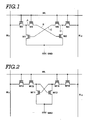
- the first embodiment of a memory cell circuit has a pair of memory transistors M1 and M2, two pairs of access transistors M3, M4, M5 and M6.
- This embodiment of the memory cell circuit is intended to accomplish improved data holding characteristics and high speed read/write operation by connecting the drains of the memory transistors M1 and M2 to junctions between series of transistors M3, M5 and M4, M6.
- the first embodiment of the memory cell circuit according to the invention is formed as showed in Fig 1.
- the pair of memory transistors M1 and M2 respectively have sources connected in common to a ground.
- the memory transistor M1 also has a drain which is connected to a first bit line BL1 via a first access transistor M3.
- the memory transistor M2 has a drain connected to a second bit line BL2 via a second access transistor M4.
- the first and second access transistors M3 and M4 have their respective gates connected to a word line WL (read line).
- each of the first and second access transistors M3 and M4 has drain connected to the corresponding one of third access transistor M5 and fourth access transistor M6.
- the third and fourth access transistors M5 and M6 have gates connected to the word line WL.
- the drains of third and fourth access transistors M5 and M6 are connected to gates of respective diagonally opposing memory transistors M1 and M2.
- the channel leak can be successfully suppressed by providing the third access transistor M5.
- the third access transistor M5 is provided in such a position that it is disposed between the points B and A, at which point A, the drain of the memory transistor M1 is connected between the drain of the first access transistor and the source of the third access transistor M5.
- the third access transistor M5 divides the potential between the point B and point A.
- the magnitude of the channel leak is exponentially related to the voltage at the junction (A) between the drain and the source of the transistors. Therefore, by dividing the voltage, the voltage at the drain-source connection of the transistors can be substantially reduced so that the value of the current leak can be markedly reduced.
- selection signal is applied to all of the gates of the access transistors M3, M4, M5 and M6 via the wordline WL.
- the first to fourth access transistors M3, M4, M5 and M6 are turned ON.
- the first to fourth access transistors M3, M4, M5 and M6 are turned ON.
- a latching operation takes place to turn off whichever one of the memory transistors M1 and M2 has lower charge in its gate and turn the other memory transistor ON. By this operation, data to be read out can be fixed.
- the noise superimposed on the signal of bit lines BL1 and BL2 in the prior art tends to influence to the data read-out from the memory circuit. That is, when the noise is superimposed on the data of the bit lines BL1 and BL2, an error voltage can enter the memory cell circuit. The error voltage tends to be directly applied to the gate of the memory transistor to corrupt the data stored in the gate.
- the memory transistor M1 is connected to the bit line BL1 via the access transistors M3 and M5 and the memory transistor M2 is connected to the bit line BL2 via the access transistors M4 and M6, so that the data content of the cell is sufficiently protected by their resistances when the access transistors M3, M4, M5 and M6 are held ON.
- the size, ie channel length, of the access transistors can be reduced.
- a shorter channel length of the access transistors allows quicker access. Consequently, higher access speeds can be achieved when the channel length of the first and the second access transistors is shortened.
- the intervals between refresh cycles can be made longer and the power consumption can be reduced.
- the illustrated embodiment of the memory cell circuit is constituted of six transistors, and has an increased number of circuit components.
- all of the transistors constituting the memory cell circuit can be NMOS transistors which require a smaller chip area than CMOS transistors (which require a well region and so forth), the overall area occupied by the first embodiment of the memory cell circuit can be equivalent to or even smaller than that in the conventional ones.
- Fig 2 shows a second embodiment of the memory cell circuit in accordance with the present invention.
- This second embodiment of the memory cell circuit is formed as a dual gate access transistor-type cell.
- This memory cell circuit has a pair of memory transistors M11 and M12; the drain of the memory transistor M11 is connected to the gate of the memory transistor M12 and the drain of the memory transistor M12 is connected to the gate of the memory transistor M11.
- the sources of transistors M11 and M12 are connected in common to a GND.
- a first and third access transistors M13 and M15 are disposed between a junction between the drain of the memory transistor M11 and the gate of the memory transistor M12, and the bit line BL1.
- second and fourth access transistors M14 and M15 are disposed between a junction between the drain of the memory transistor M12 and the gate of the memory transistor M11, and the bit line BL2.
- the memory transistors M11 and M12 and the first, second, third and fourth transistors M3, M4, M5 and M6 comprise NMOS transistors.
- the memory cell transistor of this invention is provided with the third and the fourth access transistors. Therefore, channel leak can be reduced exponentially and improvement of the data holding characteristics can be achieved.
- a memory cell transistor which comprises connections to the drains of a pair of transistors, one of the connections is connected between the first access transistor and the second access transistor and the other connection is connected between the third access transistor and the fourth access transistor, loss of data due to an error voltage can be prevented and a rapid access operation can be achieved with reduced power consumption in the refresh cycle of the memory cell circuit.
Landscapes
- Engineering & Computer Science (AREA)
- Microelectronics & Electronic Packaging (AREA)
- Computer Hardware Design (AREA)
- Dram (AREA)
- Static Random-Access Memory (AREA)
- Semiconductor Memories (AREA)
Applications Claiming Priority (2)
| Application Number | Priority Date | Filing Date | Title |
|---|---|---|---|
| JP61227447A JPS6381694A (ja) | 1986-09-26 | 1986-09-26 | メモリセル回路 |
| JP227447/86 | 1986-09-26 |
Publications (3)
| Publication Number | Publication Date |
|---|---|
| EP0262850A2 true EP0262850A2 (de) | 1988-04-06 |
| EP0262850A3 EP0262850A3 (en) | 1989-05-17 |
| EP0262850B1 EP0262850B1 (de) | 1991-12-27 |
Family
ID=16861013
Family Applications (1)
| Application Number | Title | Priority Date | Filing Date |
|---|---|---|---|
| EP87308341A Expired - Lifetime EP0262850B1 (de) | 1986-09-26 | 1987-09-21 | Speicherzellschaltung |
Country Status (5)
| Country | Link |
|---|---|
| US (1) | US4839863A (de) |
| EP (1) | EP0262850B1 (de) |
| JP (1) | JPS6381694A (de) |
| KR (1) | KR880004484A (de) |
| DE (1) | DE3775508D1 (de) |
Families Citing this family (6)
| Publication number | Priority date | Publication date | Assignee | Title |
|---|---|---|---|---|
| US5020028A (en) * | 1989-08-07 | 1991-05-28 | Standard Microsystems Corporation | Four transistor static RAM cell |
| US5814895A (en) * | 1995-12-22 | 1998-09-29 | Sony Corporation | Static random access memory having transistor elements formed on side walls of a trench in a semiconductor substrate |
| US7088606B2 (en) * | 2004-03-10 | 2006-08-08 | Altera Corporation | Dynamic RAM storage techniques |
| US7506643B2 (en) | 2006-06-30 | 2009-03-24 | Larry Holmberg | Crossbow device mount |
| JP2008153479A (ja) * | 2006-12-19 | 2008-07-03 | Rohm Co Ltd | 強誘電体電界効果トランジスタを備える半導体装置及びこれを用いた半導体集積回路装置 |
| US8634230B2 (en) * | 2011-01-28 | 2014-01-21 | Semiconductor Energy Laboratory Co., Ltd. | Semiconductor device and method for driving the same |
Family Cites Families (2)
| Publication number | Priority date | Publication date | Assignee | Title |
|---|---|---|---|---|
| US4095281A (en) * | 1976-03-04 | 1978-06-13 | Rca Corporation | Random access-erasable read only memory cell |
| JPS58147886A (ja) * | 1982-02-26 | 1983-09-02 | Mitsubishi Electric Corp | GaAs半導体記憶回路 |
-
1986
- 1986-09-26 JP JP61227447A patent/JPS6381694A/ja active Pending
-
1987
- 1987-09-21 EP EP87308341A patent/EP0262850B1/de not_active Expired - Lifetime
- 1987-09-21 DE DE8787308341T patent/DE3775508D1/de not_active Expired - Lifetime
- 1987-09-24 KR KR870010574A patent/KR880004484A/ko not_active Withdrawn
- 1987-09-28 US US07/101,441 patent/US4839863A/en not_active Expired - Fee Related
Non-Patent Citations (2)
| Title |
|---|
| HEWLETT-PACKARD JOURNAL, vol. 34, no. 8, August 1983, pages 20-24, Amstelveen, NL; J.K. WHEELER et al.: "128K-Bit NMOS dynamic RAM with redundancy" * |
| IEEE JOURNAL OF SOLID-STATE CIRCUITS, vol. SC-3, no. 3, September 1968, pages 280-285; J.H. FRIEDRICH: "A coincident-select MOS storage array" * |
Also Published As
| Publication number | Publication date |
|---|---|
| DE3775508D1 (de) | 1992-02-06 |
| JPS6381694A (ja) | 1988-04-12 |
| EP0262850B1 (de) | 1991-12-27 |
| EP0262850A3 (en) | 1989-05-17 |
| US4839863A (en) | 1989-06-13 |
| KR880004484A (ko) | 1988-06-04 |
Similar Documents
| Publication | Publication Date | Title |
|---|---|---|
| US4780850A (en) | CMOS dynamic random access memory | |
| US6259623B1 (en) | Static random access memory (SRAM) circuit | |
| US4342101A (en) | Nonvolatile semiconductor memory circuits | |
| US4791616A (en) | Semiconductor memory device | |
| US4375600A (en) | Sense amplifier for integrated memory array | |
| US5457657A (en) | High-speed sense amplifier having feedback loop | |
| JPH0160789B2 (de) | ||
| US4794571A (en) | Dynamic read-write random access memory | |
| JPH0361279B2 (de) | ||
| JP2885607B2 (ja) | 半導体メモリ | |
| US4602355A (en) | Memory circuit with noise preventing means for word lines | |
| KR910004733B1 (ko) | 데이타 버스 리셋트 회로를 지닌 반도체 기억장치 | |
| EP0262850B1 (de) | Speicherzellschaltung | |
| US4734889A (en) | Semiconductor memory | |
| US4380055A (en) | Static RAM memory cell | |
| US5515315A (en) | Dynamic random access memory | |
| US5781482A (en) | Semiconductor memory device | |
| US4779230A (en) | CMOS static ram cell provided with an additional bipolar drive transistor | |
| US4931992A (en) | Semiconductor memory having barrier transistors connected between sense and restore circuits | |
| US5838606A (en) | Three-transistor static storage cell | |
| JP2937719B2 (ja) | 半導体記憶装置 | |
| KR920001331B1 (ko) | 반도체기억장치 | |
| EP0377841B1 (de) | Integrierte Halbleiterschaltung, fähig ein Ereignis einer fehlerhaften Wirkung wegen Störungen zu verhindern | |
| EP0230385B1 (de) | Halbleiterspeicher | |
| US6246604B1 (en) | Memory array architecture, method of operating a dynamic random access memory, and method of manufacturing a dynamic random access memory |
Legal Events
| Date | Code | Title | Description |
|---|---|---|---|
| PUAI | Public reference made under article 153(3) epc to a published international application that has entered the european phase |
Free format text: ORIGINAL CODE: 0009012 |
|
| AK | Designated contracting states |
Kind code of ref document: A2 Designated state(s): DE FR GB NL |
|
| PUAL | Search report despatched |
Free format text: ORIGINAL CODE: 0009013 |
|
| AK | Designated contracting states |
Kind code of ref document: A3 Designated state(s): DE FR GB NL |
|
| 17P | Request for examination filed |
Effective date: 19891107 |
|
| 17Q | First examination report despatched |
Effective date: 19910227 |
|
| GRAA | (expected) grant |
Free format text: ORIGINAL CODE: 0009210 |
|
| AK | Designated contracting states |
Kind code of ref document: B1 Designated state(s): DE FR GB NL |
|
| PG25 | Lapsed in a contracting state [announced via postgrant information from national office to epo] |
Ref country code: NL Effective date: 19911227 Ref country code: FR Effective date: 19911227 |
|
| REF | Corresponds to: |
Ref document number: 3775508 Country of ref document: DE Date of ref document: 19920206 |
|
| EN | Fr: translation not filed | ||
| NLV1 | Nl: lapsed or annulled due to failure to fulfill the requirements of art. 29p and 29m of the patents act | ||
| PG25 | Lapsed in a contracting state [announced via postgrant information from national office to epo] |
Ref country code: GB Effective date: 19920921 |
|
| PLBE | No opposition filed within time limit |
Free format text: ORIGINAL CODE: 0009261 |
|
| STAA | Information on the status of an ep patent application or granted ep patent |
Free format text: STATUS: NO OPPOSITION FILED WITHIN TIME LIMIT |
|
| 26N | No opposition filed | ||
| GBPC | Gb: european patent ceased through non-payment of renewal fee |
Effective date: 19920921 |
|
| PGFP | Annual fee paid to national office [announced via postgrant information from national office to epo] |
Ref country code: DE Payment date: 19931130 Year of fee payment: 7 |
|
| PG25 | Lapsed in a contracting state [announced via postgrant information from national office to epo] |
Ref country code: DE Effective date: 19950601 |