EP0263487A2 - Appareil d'ajustement d'un axe optique pour microscope électronique - Google Patents
Appareil d'ajustement d'un axe optique pour microscope électronique Download PDFInfo
- Publication number
- EP0263487A2 EP0263487A2 EP87114581A EP87114581A EP0263487A2 EP 0263487 A2 EP0263487 A2 EP 0263487A2 EP 87114581 A EP87114581 A EP 87114581A EP 87114581 A EP87114581 A EP 87114581A EP 0263487 A2 EP0263487 A2 EP 0263487A2
- Authority
- EP
- European Patent Office
- Prior art keywords
- image
- optical axis
- marker
- adjusting apparatus
- amount
- Prior art date
- Legal status (The legal status is an assumption and is not a legal conclusion. Google has not performed a legal analysis and makes no representation as to the accuracy of the status listed.)
- Withdrawn
Links
Images



Classifications
-
- H—ELECTRICITY
- H01—ELECTRIC ELEMENTS
- H01J—ELECTRIC DISCHARGE TUBES OR DISCHARGE LAMPS
- H01J37/00—Discharge tubes with provision for introducing objects or material to be exposed to the discharge, e.g. for the purpose of examination or processing thereof
- H01J37/26—Electron or ion microscopes; Electron or ion diffraction tubes
- H01J37/261—Details
- H01J37/265—Controlling the tube; circuit arrangements adapted to a particular application not otherwise provided, e.g. bright-field-dark-field illumination
Definitions
- the present invention relates to an optical axis adjusting apparatus for an electron microscope, and more particularly to such an apparatus for aligning the optical axis of a radiation lens system and the optical axis of an imaging lens system with each other.
- the adjustment of the optical axes including the optical axis alignment through current change (current alignment) or the optical axis alignment through voltage change (voltage alignment) is carried out. Namely, if an objective lens current or an accelerating voltage is changed, a final image moves circumferentially or radially about a certain point, called a current center or voltage center, which does not move.
- the optical axis adjustment is performed so as to position the current or voltage center to a center of the final image or usually the center of a flourescent screen to which the final image is projected for observation.
- the period of the current or voltage change is quickened to utilize an after-image of the flourescent screen being observed, the movement of the image is not be observed but only the blurring of the image is observed. In that case, therefore, it may be possible that the current or voltage center can be easily found out. But, the period of the current or voltage change is limited to several hertz at the highest because of a large time constant of the objective lens coil or the accelerating voltage circuit. Actually, therefore, any movement of the image is involved or observed and hence the current or voltage center cannot be easily found out.
- An object of the present invention is to provide an optical axis adjusting apparatus for an electron microscope capable of easily carrying out the optical axis adjustment by easily finding out the current or voltage center.
- This object is achieved by changing an objective lens current or an accelerating voltage, storing a plurality of final images in the course of the current or voltage change into image memories to thereafter integrate or average the stored final images or storing such final images into a image memory while integrating or averaging them, and displaying a blurred image obtained by the integration or averaging to perform the optical axial alignment.
- an electron beam 21 emitted from an electron gun 1 is condensed by a radiation lens system 2 to irradiate a specimen 4.
- the electron beam transmitted through the specimen 4 is enlarged by an imaging (or image-forming) lens system 5 to form a final image on a flourescent screen (or phosphor plate) 6.
- the final image is taken in (or picked up) by a television (TV) camera 10 and converted into an electric signal through a controller 11.
- the controller 11 has a function of a power source for the TV camera 10 as well as a function of an amplifier for an input video signal.
- the input video signal is converted into a digital signal through an A/D converter 12 and stored in an image memory 14a through an operating unit 13.
- the operating unit 13 operates to sum and average a video signal being now inputted and a preceding video signal of the corresponding picture element previously stored in the image memory 14a and to store the average value in the image memory 14a again.
- This operation may be also performed by a microprocessor in accordance with a program, as will be described in later.
- a multiplicity of image memories 14a, --- 14b are prepared for making it possible to store respective input images into a plurality of image memories and to prepare an image memory for storing the result of sum of images stored in the plural image memories.
- the contents of one of the image memories are selected by an output change-over controller 19 and delivered to a CRT monitor 20 through a D/A converter 17 to display as an image.
- These controls are made by a microprocessor 16b in accordance with a program which is previously stored in a memory 15b including ROM/RAM.
- the above-described TV system is known by H. Kobayashi et al "OBSERVATION AND RECORDING OF TEM IMAGES THROUGH TV-SYSTEM", pp. 453-454 of Proc. XI-th Int. Cong. on Electron Microscopy, Kyoto, 1986.
- the accelerating voltage, lens currents and electron beam deflector 3 of the electron microscope are controlled by a microprocessor 16a through D/A converters 7a to 7g. This control is made in accordance with a program which is previously stored in a memory 15a including ROM/RAM.
- Reference numeral 8 designates a transformer for the accelerating voltage, and numerals 9a to 9f designate power sources. Since these circuits are known by U.S. Patent No. 4,531,057, further explanation will be omitted.
- Reference numeral 18 designates a deflection input device for inputting the amount of deflection of an electron beam.
- the amount of electron beam deflection by the electron beam deflector 3 is set in accordance with an input from the deflection input device 18.
- Numeral 23 designates a cross marker memory for storing a cross marker to be displayed on the CRT monitor 20.
- a cross point of the marker can be moved by an input from a cross marker input device 24.
- An information communication is made between the microprocessors 16a and 16b so that the microprocessor 16b causes the TV system to take in an image in synchronism with the change of a magnetization current supplied to an objective lens 5a from the microprocessor 16a or the change of an accelerating voltage supplied to the electron gun 1 from the microprocessor 16a. Further, a change of the amount of deflection by the electron beam deflector 3 is communicated from the microprocessor 16a to the microprocessor 16b to alter the contents of the cross marker memory 23, thereby moving the cross marker on the CRT monitor 20.
- the objective lens current or the accelerating voltage is changed stepwise under the control of the microprocessor 16a in accordance with a program stored in the ROM 15a.
- the microprocessor 16b takes an image in the image memory for each step in synchronism with the stepwise change of the current or voltage.
- the taken-in image with its intensity divided by the total number of images to be taken in is stored in one image memory while being added by the operating unit 13 to the image stored in the same image memory at the preceding step.
- the image thus stored in the image memory is displayed on the CRT monitor 20.
- the images for the respective steps are taken in the image memories 14a, ---.
- all of those images are integrated and averaged by the microprocessor 16b and the resulting average image in a blurred form is stored in the image memory 14b.
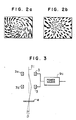
- Fig. 3 is a view for explaining an action of the electron beam deflector 3 for aligning the optical axes of the radiation and imaging lens systems with each other when those axes are tilted with respect to each other.
- a dotted line represents the optical axis of the radiation lens system and a dotted and chain line represents the optical axis of the imaging lens system.
- the electron beam 21 is first deflected by an upper deflection coil 3a to the left seen in a traveling direction of the electron beam and thereafter deflected by a lower deflection coil 3b to the right seen in the beam traveling direction, as shown by a solid line, thereby aligning the optical axis of the radiation lens system with respect to that of the imaging lens system.
- this blurred image and the cross marker are read from the image memory 14a and the cross marker memory 23 respectively and displayed on the CRT monitor 20 in an overlapping manner as shown in Fig. 4a or 4c.
- the electron beam deflector 3 changes the amount of deflection of the electron beam on the basis of the deflection signal and at the same time the microprocessor 16b operates to move the cross marker on the CRT monitor 20 in synchronism with the deflection of the electron beam, thereby effecting a center axis alignment so that a cross point of the cross marker coincides with the current center or voltage center, as shown in Fig. 4b or 4d. If an image on the fluorescent screen 6 is taken in and displayed on the CRT monitor 20, the current center or voltage center of the displayed image is positioned at the center of an image screen of the CRT monitor 20, as shown in Fig. 4e or 4f.
- the displayed image is a stationary image however moved by the electron beam deflector 3 the electron beam may be and hence however moved an image on the fluorescent screen 6 may be.
- the displayed cross marker is moved in an interlocking relation with the deflection of the electron beam by the deflector 3 in a direction reverse to the direction of movement of the image on the flourescent screen 6 but by the same distance as the image movement amount. Accordingly, if the cross point of the cross marker is moved on the CRT monitor 20 from the center of the CRT to the current center or voltage center, the current center or voltage center of the image on the flourescent screen 6 is to be positioned at the center of the fluorescent screen 6.
- a correspondence relation between the direction and amount of deflection of the electron beam and the direction and amount of movement of the cross marker can be previously determined by experiments or calculation.
- the microprocessor 16a When the amount ⁇ x (or ⁇ y ) of deflection for an electron beam in a x- (or y-) direction is inputted from the deflection input device 18, the microprocessor 16a reads this deflection amount to add it to the current or present deflection amount D x (or D g ).
- the value of D x,y + ⁇ x,y is supplied to the electron beam deflector 3 through the D/A converter 7d.
- the deflection amount D represents a deflection angle, as is shown in Fig. 3.
- a final image on the fluorescent screen 6 at that time is displayed on the CRT monitor 20 to find out the current or voltage center.
- the amount ⁇ X (or ⁇ Y ) of movement of the current or voltage center of the displayed image from the current of voltage center in the case of the preceding deflection amount D x,y is determined.
- ⁇ X,Y and ⁇ x,y is preliminarily determined by experiments and stored as a linear function in the memory 15b.
- the amount of deflection of the electron beam is D ⁇ x,y + ⁇ x,y .
- the current or voltage center of that image is to be positioned at a center of the image screen of the CRT, as is shown in Fig. 4e or 4f.
- the current or voltage alignment is completed.
- the current or voltage alignment can be very easily attained by merely adjusting the deflection amount inputted from deflection input device so as to move the cross marker to the current or voltage center as shown in Fig. 4b or 4d.
- Fig. 5 is a flow chart showing an embodiment of the image taking-in operation.
- the number n of taking-in of image i.e. the number n of steps in a stepwise change of the lens current or accelerating voltage is set into the RAM 15b, and initialization including the clearing of a counter i for counting the number of images taken in and the clearing of the image memories 14a, --- 14b is made.
- step 52 one (1) count is added to the counter i .
- step 53 whether the count value of the counter i is smaller than n or not is judged. Since now is the first time, the judgement of YES is made to proceed to step 54 in which the accelerating voltage V is reduced by a minute voltage ⁇ V volts.
- a taken-in video signal is divided by the number n of taking-in of image and the result is added to a signal of the corresponding picture element in the image memory 14a (step 55).
- this value of sum is stored in the image memory 14a again. Since now is the first time, one n-th of the video signal is only written in the image memory 14a the contents of which are zero.
- the process is returned to step 52 in which the counter i is advanced by one count again. In this manner, the above-mentioned operation is repeated.
- step 53 judges that the count value is equal to n , the process goes to step 57 in which the image S in the image memory 14a is displayed on the CRT monitor 20.
- Fig. 6 is a flow chart showing another embodiment of the image taking-in operation.
- interlock ratios are designated in step 71. Namely, provided that ⁇ X and ⁇ Y are the amounts of movement of an image on the fluorescent screen 6 when the changes of ⁇ x and ⁇ y in deflection amount in x- and y-directions are given to the electron beam deflector 3, the microprocessor 16a sets to the RAM 15b the interlock ratios represented by ⁇ X / ⁇ x and ⁇ Y / ⁇ y .
- step 72 thereafter, while a cross marker is observed, deflection amounts ⁇ and ⁇ in a direction in which a cross point of the cross marker coincides with the current or voltage center are inputted from the deflection input device 18.
- step 73 the sums D x + ⁇ and D y + ⁇ of the current or present deflection amounts D x and D y and the input deflection amounts ⁇ and ⁇ are supplied to the electron beam deflector 3.
- the deflection amount represents a deflection angle indicated by D in Fig. 3.
- step 74 the deflection amounts ⁇ x ⁇ and ⁇ y ⁇ are multiplied by the interlock ratios K x and K y respectively to determine the movement amounts ⁇ x ⁇ and ⁇ y ⁇ on the fluorescent screen 6.
- step 75 ⁇ x ⁇ and ⁇ y ⁇ are multiplied by a magnification M to determine the movement amounts ⁇ X ⁇ and ⁇ Y ⁇ of an image on the fluorescent screen 6 and hence on the CRT monitor 20.
- step 76 the movement amounts ⁇ X ⁇ and ⁇ Y ⁇ are sent.
- the microprocessor 16b receives the movement amounts ⁇ X ⁇ and ⁇ Y ⁇ (step 77) and moves the cross marker in a direction reverse to the direction of movement of the image by distances equal to ⁇ X ⁇ and ⁇ Y ⁇ (step 78).
- the process may be returned from step 78 to step 72 since the operation in step 72 is carried out while observing the image displayed in step 78. If an image on the fluorescent screen 6 is displayed on the CRT monitor 20 after the above-mentioned procedure has been completed, the image can be displayed with a current or voltage center thereof positioned at the center of the CRT monitor screen.
- a method can be employed in which the deflection amount by the deflector 3 is controlled interlocking with the amount of movement of the cross marker by an input from the cross marker input device 24.
- An example of such a control is shown in Fig. 8.
- the microprocessor 16b operates in step 81 so that the amounts ⁇ X ⁇ and ⁇ Y ⁇ of movement of the cross marker from the cross marker input device 24 by which the cross marker on the CRT monitor 20 is to be moved to the current or voltage center are written in the cross marker memory 23.
- the cross marker is moved by - ⁇ X ⁇ and - ⁇ Y ⁇ in accordance with the written marker movement amounts.
- the marker movement amounts are sent to the microprocessor 16a (step 83).
- the microprocessor 16a receives the marker movement amounts ⁇ x ⁇ and ⁇ Y ⁇ (step 84), dividing them by the magnification M to determine the amounts ⁇ x ⁇ and ⁇ y ⁇ of movement on the fluorescent screen 6 when it is assumed that the magnification is 1 (step 85), and thereafter dividing the movement amounts ⁇ x ⁇ and ⁇ y ⁇ by the interlock ratios K x and K y to determine the deflection amounts ⁇ x ⁇ and ⁇ y ⁇ (step 86).
- step 87 the process is terminated by altering the deflection amounts by the electron beam deflector 3 from D x and D y to D x + ⁇ x ⁇ and D y + ⁇ y ⁇ . If after the termination of this optical axis adjustment operation an image on the fluorescent screen 6 is displayed on the CRT monitor 20, the image can be displayed with a current or voltage center thereof positioned at the center of the CRT monitor screen.
- the directions of coordinates x and y of the deflector 3 are the same as those of coordinates X and Y on the fluorescent screen 6.
- those directions are different from each other because of the rotation of an image due to the magnetization of the imaging lens system.
- ⁇ is a difference in angle between the x- and y- directions and the X and Y directions.
- the movement of the cross marker has been made interlocking with the deflection amount.
- a known image stroke technique can be used to process images taken in the image memory so that only the image is moved on the CRT monitor 20 while maintaining the cross marker at the center of the CRT monitor screen. In that case, it may be not necessary to display the cross marker.
- the current or voltage center can be easily found out and hence the optical axis adjustment can be easily carried out.
- the operability of the electron microscope can be greatly improved, which is a great merit for an electron microscope having a TV camera mounted thereto.
Landscapes
- Chemical & Material Sciences (AREA)
- Analytical Chemistry (AREA)
- Electron Sources, Ion Sources (AREA)
Applications Claiming Priority (2)
| Application Number | Priority Date | Filing Date | Title |
|---|---|---|---|
| JP61237967A JPH073774B2 (ja) | 1986-10-08 | 1986-10-08 | 電子顕微鏡 |
| JP237967/86 | 1986-10-08 |
Publications (2)
| Publication Number | Publication Date |
|---|---|
| EP0263487A2 true EP0263487A2 (fr) | 1988-04-13 |
| EP0263487A3 EP0263487A3 (fr) | 1989-08-30 |
Family
ID=17023118
Family Applications (1)
| Application Number | Title | Priority Date | Filing Date |
|---|---|---|---|
| EP87114581A Withdrawn EP0263487A3 (fr) | 1986-10-08 | 1987-10-06 | Appareil d'ajustement d'un axe optique pour microscope électronique |
Country Status (3)
| Country | Link |
|---|---|
| US (1) | US4788425A (fr) |
| EP (1) | EP0263487A3 (fr) |
| JP (1) | JPH073774B2 (fr) |
Cited By (3)
| Publication number | Priority date | Publication date | Assignee | Title |
|---|---|---|---|---|
| EP0488214A3 (en) * | 1990-11-27 | 1992-07-15 | Hitachi, Ltd. | Electron microscope |
| EP1116932A2 (fr) * | 2000-01-14 | 2001-07-18 | Leica Microsystems Wetzlar GmbH | Appareil de mesure et méthode pour mesurer des structures sur un substrat |
| EP1432009A3 (fr) * | 2002-12-20 | 2010-06-23 | Hitachi High-Technologies Corporation | Méthode et appareil d'exposition avec faisceaux d'électrons |
Families Citing this family (14)
| Publication number | Priority date | Publication date | Assignee | Title |
|---|---|---|---|---|
| JP2712184B2 (ja) * | 1987-07-29 | 1998-02-10 | 株式会社ニコン | 荷電粒子線の軸調整装置 |
| JP2686492B2 (ja) * | 1988-12-12 | 1997-12-08 | 株式会社日立製作所 | 透過形電子顕微鏡の照射位置決め方法 |
| CA1308203C (fr) * | 1989-06-01 | 1992-09-29 | Nanoquest (Canada) Inc. | Dispositif compensateur d'amplification |
| JPH053009A (ja) * | 1991-06-21 | 1993-01-08 | Jeol Ltd | 電子顕微鏡における軸上コマ補正方式 |
| US5389858A (en) * | 1992-07-16 | 1995-02-14 | International Business Machines Corporation | Variable axis stigmator |
| JP3400608B2 (ja) * | 1995-06-01 | 2003-04-28 | 株式会社日立製作所 | 走査電子顕微鏡 |
| US5747814A (en) * | 1996-12-06 | 1998-05-05 | International Business Machines Corporation | Method for centering a lens in a charged-particle system |
| US6278114B1 (en) | 1997-12-19 | 2001-08-21 | Kabushiki Kaisha Toshiba | Method and apparatus for measuring dimensions of a feature of a specimen |
| JP3522121B2 (ja) * | 1998-09-02 | 2004-04-26 | 日本電子株式会社 | 電子顕微鏡 |
| US6476398B1 (en) * | 1999-03-05 | 2002-11-05 | Applied Materials, Inc. | Beam automation in charged-particle-beam systems |
| JP5066056B2 (ja) * | 2008-10-31 | 2012-11-07 | 株式会社日立ハイテクノロジーズ | 試料観察方法、及び電子顕微鏡 |
| JP5409511B2 (ja) * | 2010-05-20 | 2014-02-05 | 株式会社日立ハイテクノロジーズ | 電子顕微鏡、および電子顕微鏡の光軸調整方法 |
| JP6783071B2 (ja) * | 2016-05-20 | 2020-11-11 | 株式会社日立ハイテク | 荷電粒子線装置 |
| JP7114417B2 (ja) * | 2018-09-10 | 2022-08-08 | 日本電子株式会社 | 電子顕微鏡および電子顕微鏡の調整方法 |
Family Cites Families (11)
| Publication number | Priority date | Publication date | Assignee | Title |
|---|---|---|---|---|
| US3917946A (en) * | 1972-04-12 | 1975-11-04 | Philips Corp | Electron-optical device for the recording of selected diffraction patterns |
| JPS521869B2 (fr) * | 1972-07-11 | 1977-01-18 | ||
| DE2535510C2 (de) * | 1975-08-06 | 1977-09-08 | Siemens AG, 1000 Berlin und 8000 München | Elektronenstrahl-Rastergerät zur Strukturanalyse von Präparaten |
| DE2542356C2 (de) * | 1975-09-19 | 1977-10-20 | Siemens AG, 1000 Berlin und 8000 München | Verfahren zur Fokussierung der Objektivlinse eines Korpuskular-Durchstrahlungs-Rastermikroskops und Einrichtung zur selbsttätigen Durchführung des Verfahrens, sowie Anwendung |
| JPS57212754A (en) * | 1981-06-24 | 1982-12-27 | Hitachi Ltd | Electron-beam controller for electron microscope |
| JPS58152354A (ja) * | 1982-03-05 | 1983-09-09 | Hitachi Ltd | 電子顕微鏡の軸調整装置 |
| DE3325855A1 (de) * | 1983-07-18 | 1985-01-31 | Max-Planck-Gesellschaft zur Förderung der Wissenschaften e.V., 3400 Göttingen | Einrichtung zum erzeugen eines signales entsprechend einem faltungsprodukt zweier funktionen |
| GB8410168D0 (en) * | 1984-04-18 | 1984-05-31 | Smith K C A | Charged-particle beams |
| JPS614144A (ja) * | 1984-06-15 | 1986-01-10 | Jeol Ltd | 電子顕微鏡による回折パタ−ン表示方法 |
| US4680469A (en) * | 1984-08-17 | 1987-07-14 | Hitachi, Ltd. | Focusing device for a television electron microscope |
| JPS61168852A (ja) * | 1985-01-23 | 1986-07-30 | Hitachi Ltd | 透過形電子顕微鏡の焦点合せ装置 |
-
1986
- 1986-10-08 JP JP61237967A patent/JPH073774B2/ja not_active Expired - Fee Related
-
1987
- 1987-10-06 EP EP87114581A patent/EP0263487A3/fr not_active Withdrawn
- 1987-10-07 US US07/105,253 patent/US4788425A/en not_active Expired - Fee Related
Cited By (4)
| Publication number | Priority date | Publication date | Assignee | Title |
|---|---|---|---|---|
| EP0488214A3 (en) * | 1990-11-27 | 1992-07-15 | Hitachi, Ltd. | Electron microscope |
| US5243191A (en) * | 1990-11-27 | 1993-09-07 | Hitachi, Ltd. | Electron microscope |
| EP1116932A2 (fr) * | 2000-01-14 | 2001-07-18 | Leica Microsystems Wetzlar GmbH | Appareil de mesure et méthode pour mesurer des structures sur un substrat |
| EP1432009A3 (fr) * | 2002-12-20 | 2010-06-23 | Hitachi High-Technologies Corporation | Méthode et appareil d'exposition avec faisceaux d'électrons |
Also Published As
| Publication number | Publication date |
|---|---|
| JPH073774B2 (ja) | 1995-01-18 |
| US4788425A (en) | 1988-11-29 |
| EP0263487A3 (fr) | 1989-08-30 |
| JPS6394544A (ja) | 1988-04-25 |
Similar Documents
| Publication | Publication Date | Title |
|---|---|---|
| US4788425A (en) | Optical axis adjusting apparatus for electron microscope | |
| USRE41665E1 (en) | Object observation apparatus and object observation | |
| EP1235251B1 (fr) | Appareil a faisceau electronique | |
| JPH09330871A (ja) | 電子ビーム露光システム及びそれを用いたデバイス製造方法 | |
| CZ20022290A3 (cs) | Prohlížecí systém k zobrazení předmětu, který může být uspořádán v rovině, vychylovací zařízení a způsob jeho provozu | |
| JPH11509972A (ja) | 粒子光学機器のレンズ収差補正用補正装置 | |
| EP0566963A2 (fr) | Appareil de production d'une image échantillon | |
| EP0068896A2 (fr) | Image sans distortion et image sans rotation d'un microscope électronique | |
| JP2001510624A (ja) | 粒子光学的装置の動作方法 | |
| US5747814A (en) | Method for centering a lens in a charged-particle system | |
| US5243191A (en) | Electron microscope | |
| JPH10255709A (ja) | 画像検査装置 | |
| US5012109A (en) | Charged particle beam apparatus | |
| JP2002343294A (ja) | 複合電子顕微鏡 | |
| JP2000357481A (ja) | 走査型荷電粒子ビーム装置における試料像観察方法 | |
| US6573502B2 (en) | Combined electron microscope | |
| JPH11195590A (ja) | マルチ電子ビーム露光方法及び装置、ならびにデバイス製造方法 | |
| JPH10256136A (ja) | 荷電ビーム露光装置 | |
| US3917946A (en) | Electron-optical device for the recording of selected diffraction patterns | |
| US4439681A (en) | Charged particle beam scanning device | |
| US5767515A (en) | Rule based control for charged-particle beam instrument | |
| JPH09330870A (ja) | 電子ビーム露光装置及びその露光方法 | |
| JPH09260238A (ja) | 荷電粒子ビーム装置 | |
| JP3409961B2 (ja) | 走査電子顕微鏡 | |
| US4775790A (en) | Transmission electron microscope |
Legal Events
| Date | Code | Title | Description |
|---|---|---|---|
| PUAI | Public reference made under article 153(3) epc to a published international application that has entered the european phase |
Free format text: ORIGINAL CODE: 0009012 |
|
| 17P | Request for examination filed |
Effective date: 19871006 |
|
| AK | Designated contracting states |
Kind code of ref document: A2 Designated state(s): DE GB NL |
|
| PUAL | Search report despatched |
Free format text: ORIGINAL CODE: 0009013 |
|
| AK | Designated contracting states |
Kind code of ref document: A3 Designated state(s): DE GB NL |
|
| 17Q | First examination report despatched |
Effective date: 19920703 |
|
| STAA | Information on the status of an ep patent application or granted ep patent |
Free format text: STATUS: THE APPLICATION HAS BEEN WITHDRAWN |
|
| 18W | Application withdrawn |
Withdrawal date: 19930112 |
|
| RIN1 | Information on inventor provided before grant (corrected) |
Inventor name: KOBAYASHI, HIROYUKI |